

Page 1

Principle and Maintenance of DK1010S
CONTENTS
Chapter I Overview of DK1010S
1、Description of Functions
2、Block Diagram of Player
3、Composition of IC for Player
Chapter II Operating Principle of Servo Circuit
1、Processing Procedure of Digital Signal
2、Processing Procedure of Control Signal
Chapter III Operating Principle of Decoding Circuit
1、Control Circuit of System
2、Audio and Video Output Circuit
Chapter IV Operating Principle of Power Board
1、Block Diagram
2、Operating Principle of Circuits
Chapter V Operating Principle of Panel
1. Operating Principle
Chapter VI Troubleshooting
Appendix: Functions of IC Pins
Page 2
Important prompt:
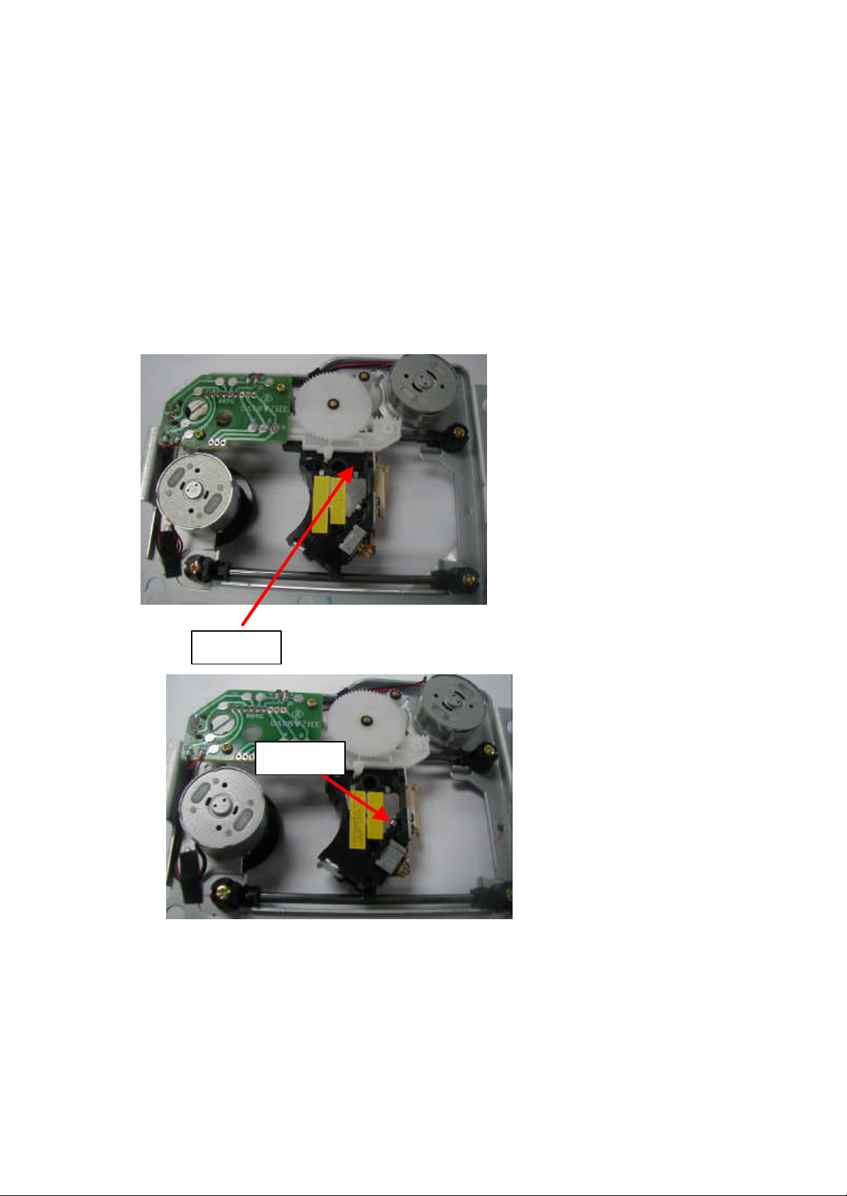
This type player employs two kinds of decks, SF-HD62 and SF-HD60, and
corresponding software of these two types of decks are different, therefore please
pay special attention during deck changing in the maintenance. Corresponding decks
should be changed with the same type of original ones, otherwise the player will be
out of order. Identification of decks is shown as figures:
SF-HD62
SF-HD60
In addition, you should also pay special attention to correspond ing problem, if the
identification of the original software is ROMDAV938-0A (16M), then it should be
changed with ones of the same identification. It is the same as to software with
Page 3

identification of ROMDK1010S -0A (16M).
This maintenance manual can be applied to player models of DK1010S, DK1020S,
DK1030S, DK1040S, DK1015S, etc.
Operating Principle Analysis of DK1010S
Chapter I Overview of DK1010S
DK1010S is a medium- low-grade model integrating with video disc
and power amplifier, with the following major features:
1. The layer adopts “Sanyo loader+MT1389” solution;
2. The power amplifier adopts the digital power amplification circuit,
with the power IC of TAS5112DFD; it has low distortion level;
3. The audio process adopts TAS5508 , with high integration and high
performance and price ratio;
4. It has the function of radio reception, and the tuner adopts Sanzhenxing
DTS-44K(CE)module;
5. The power supply adopts the switching power, with compactness, high
efficiency and stable performance;
6. Equipped with SCART(CVBS/RGB)port;
7. Accessory channel input/output function;
8. Headphone output function;
9. Karaoke and automatic accompaniment function
10. “RDS” function;
Page 4
focus
track
power
VGA
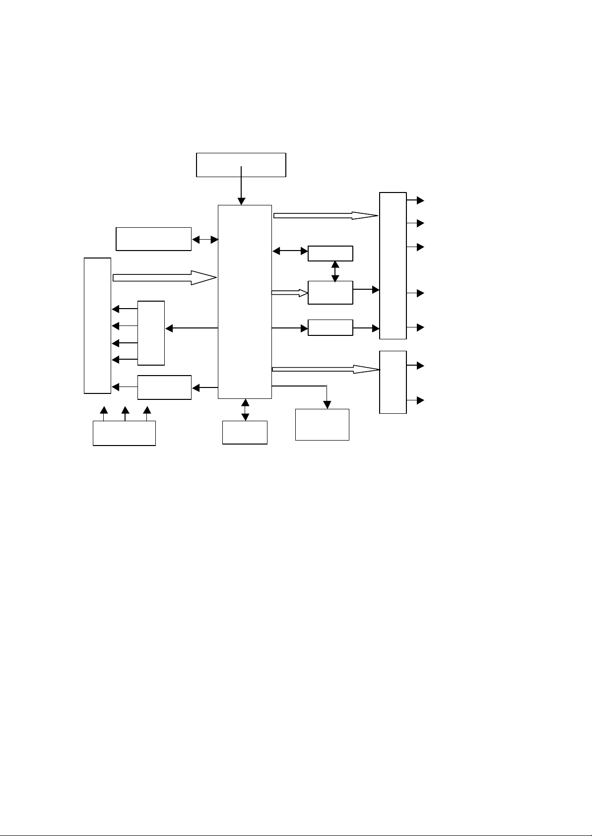
II. Block Diagram of DK1010S Complete Player and IC Function Table:
29LV160BE
16M ROM
Sany
deck
main
BA5954
feed
load
Servo
load drive
Power
Radio reception head
MT1389
MPEG decoder
Digital signal
Digital servo
SDRAM
Figure 1
AT24C02
status
4340,7265
Audio D/A,
HCU04
Panel
Refor
AV output circuit
Progressive
composite
Y/Cb/Cr
fiber,
Y/Pb/Pr
S terminal
6-way
Page 5
III. Function Table of ICs for DK1010S
Circuit
Board
Deck Sanyo Pick-up of disc signal
Main
Board
No Name Function
RF signal processing, digital signal
U201 MT1389
U202 AT24C02 Series EEPROM, status memory
U205 HCU04 Hex inverter
U209 LM1117MP-1.8 1.8v voltage -regulated power supply
U211 AE45164016 64Mbit SDRAM
U214 29LV160BE 16Mbit FLASH ROM
U302 D5954 4-channel servo driver circuit
processing, servo processing, MPEG
decoding, line scan, system control
Panel
Power
Board
Amplifier
board
N102 S0793 Panel control, VFD display drive
N103 REMOT Remote receptor
U501
U502 HS817 Photo-electric coupler
U503 HA17431 2.5V reference voltage comparator
U11 LM7805
U505 0880 Switching power circuit
U506 HS817 Photo-electric coupler
U507 LM431 2.5V reference voltage comparator
N12 5508 Digital signal processing
N13/14 5112 Power amplification
N8/9 TLV272 Operational amplification
N10/11 RC4580 Digital signal amplification
0380 Switching power circuit
5V 3-terminal voltage -regulated
power supply
Chapter II Operating Principle of Servo Circuit
I. Digital Signal Processing Procedure
DK1010S adopts Sanyo double beam super error correction deck and MTK decoding solution,
and its servo circuit mainly consists of preposition signal processing, digital servo processing,
digital signal processing IC MT1389 and driver circuit BA5954. MT1389 is also a main part of the
decoding circuit.
The A, B, C, D, E, F, SA, SB and RFO signal transmitted from the deck are mainly inputted
Page 6
through the 2-13 pins of MT1389, and after amplifying treatment of built-in amplifier of MT 1389,
the signals are treated in two parts within MT1389:
After being processed by the internal digital servo signal circuit of MT1389, part of the signal
forms into corresponding servo control signal, and output focus (FOSO), tracking (TRSO), main
shaft (DMSO) and feed (FMSO) servo control signal from the P42, P41, P37 and P38 of MT1389
and send them to the driver circuit BA5954 to amplify the drive. After drive amplification, the
signals will drive the focus coil, tracking coil, main shaft motor and feed motor. The focus and
tracking servo s will be used to adjust the object lens and enable laser beam to identify signal from
compact disc correctly; the feed servo will be used to drive the laser head to move longitudinally,
and scan the compact disc; the main shaft servo is used to control the main shaft motor to read the
signals in constant linear speed and drive the disc to rotate.
After being processed by the internal VGA voltage-controlled amplifier of MT1389 in
amplification and bala nce frequency compensation; another part of the signals is converted into
digital signal by the internal A/D converter. When the deck reads the CD/VCD signals, these
signals will be EFM demodulated in MT1389, and after accomplishing CIRC error regulation in
internal MT1389, output to the next grade to carry out audio and video decoding; when the deck
reads the DVD signals, these signals will be ESM demodulated in MT1389, and after
accomplishing RSPC error regulation in internal MT1389, output to the next grade to carry out
audio and video decoding.
II. Processing Procedure of Control Signal
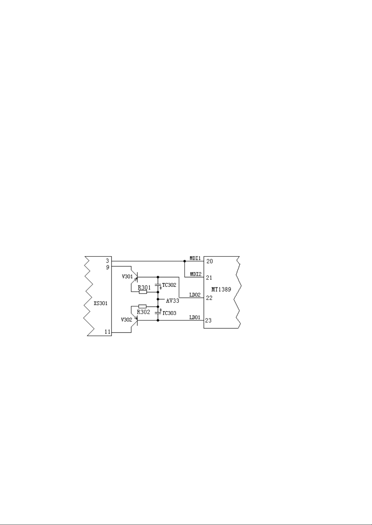
1. Automatic control of laser power, with the circuit shown as the Figure II:
Figure II
MT1389 is integrated with APC (automatic light power control) circuit. Its Pin 20 is the pin for
inputting VCD laser power rate detection signal, the Pin 21 is the pin for inputting DVD laser
power rate detection signal, and the Pin 23 is the pin for outputting VCD laser power rate drive
control. When the Pin 23 finds that the laser output power rate is too strong, the output voltage on
Pin 23 will increase after the processing of internal circuit of MT1389, and then the conduction
degree of V302 (2SB1132) and the voltage on its integration polar will decrease, which
consequently lead to the decrease of voltage supplied to the laser tube, the weakening of laser head
lighting, and thus achieve the automatic adjustment on laser output power. The Pin 22 is the pin for
outputting DVD laser power drive control, with the specific control procedure similar to that of
VCD.
2. The tray open/close control circuit is shown as the Figure III:
Page 7
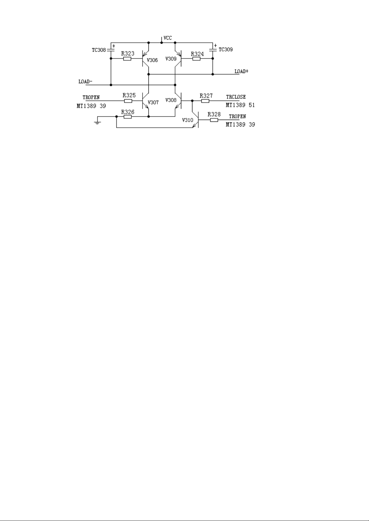
Figure III
Different from the circuit in former MTK solution, the MT1389 is integrated with preposition
signal processing circuit, so the tray open/close control signals are accomplished by MT1389, that
is to say, the close control signal is accomplished by the Pin 51 of MT1389, while the open control
signal by Pin 39 of MT1389.
When we press the open button, the Pin 51 of MT1389 is in high power level, while the Pin 39 is
in low power level, and then the triode V308 will be on-state. Through resistor R323, the base of
V306 will be made to be in low power level, and V306 will be on-state, with the current direction
as the following figure:
Power voltage VCC ? V306E-C junction ? motor negative terminal
LOAD- ? motor positive Load +? V308 C-E junction ? grounding
So the motor will rotate clockwise to accomplish the action of tray closing.
When we press the open button, the Pin 51 of MT1389 is in low power level, while the Pin 39 is in
high power level, and then the triode V307 will be conducted. Through resistor R324, the base of
V309 will be made to be in low power level, and V309 will be conducted, with the current
direction as the following figure:
Power voltage VCC ? V309E-C junction ? motor negative terminal
LOAD- ? motor positive Load +? V307 C-E junction? grounding
So the motor will rotate anti-clockwise to accomplish the action of tray opening.
3. The main shaft motor braking circuit is as the Figure IV:
To prolong the lifespan of motor and reduce the influence of start-up impact current, with the
installation of disc, our R&D personnel design the main shaft motor to be in the state of constant
operation, so that even if the STOP button is pressed, the disc will not be stopped. Therefore, when
we press the OPEN button, a braking signal is required to stop the rotation of main shaft motor
immediately to accomplish the opening action in a short time.
Page 8
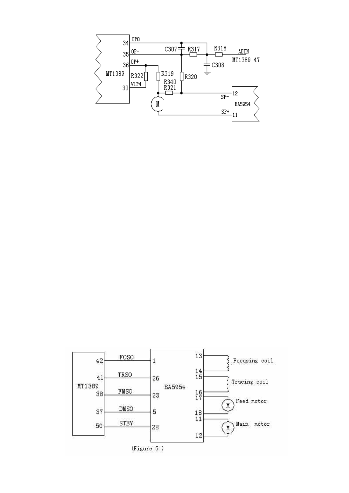
Figure IV
During playing, if we press the OPEN button, the main shaft drive signal will disappear, and
because of inertia, the main shaft motor is still in operation. As the electromotive force generated
in the operation of motor receives the induction voltage on sampling resistors R321 and R340,
which, through the resistor R319 and R320, is added to the Pin 36 and Pin 35 of MT1389, and
outputted from the Pin 34 after internal processing for amplification in MT1389, and delivered to
Pin 47 of MT1389 through R318. After the internal A/D conversion and corresponding processing,
an instant motor reversal braking signal will be outputted from the Pin 37 of MT1389 to stop the
rotation of main shaft motor immediately, so as to ensure the standstill of the disc when opening
the player.
III. Servo drive circuit
The servo drive of the player is accomplished through a piece of 4-channel dedicated drive circuit
BA5954, with the circuit as Figure V:
The 4 servo control signals generated in digital servo circuit processing of MT1389, i.e. focusing
control FOSO, tracking control TRSO, f eed control FMSO and main shaft control DMSO signals,
are added to the pins 1, 26, 23 and 5 of BA5954 respectively, and after drive amplification of
BA5954, the focusing and tracking drive signals will be outputted from the pins 13 and 14 and
pins 15 and 16 of BA5954 respectively, and added to the focusing and tracking coils to drive the
light head to accomplish the actions of focusing and tracking.
The feed and main shaft drive signals will be outputted from the pins 17 and 18 and pins 11 and 12
of BA5954 respectively, and added to the feed motor and main shaft motor to drive the light head
to move longitudinally and enable the disc to rotate in constant linear speed.
Page 9
The STBY on Pin 28 of BA5954 is an output-enabling signal, and only when the pin is in
high power level, there will be output of drive voltage on the output terminal.
Chapter III Operating Principle of Decoding Circuit
The decoding circuit of the player mainly consists of decoding chips (including MT1389, SDRAM
AE45164016 and FLASH ROM 29LV160BE) and audio DAC CS4360.
I. Control Circuit of System
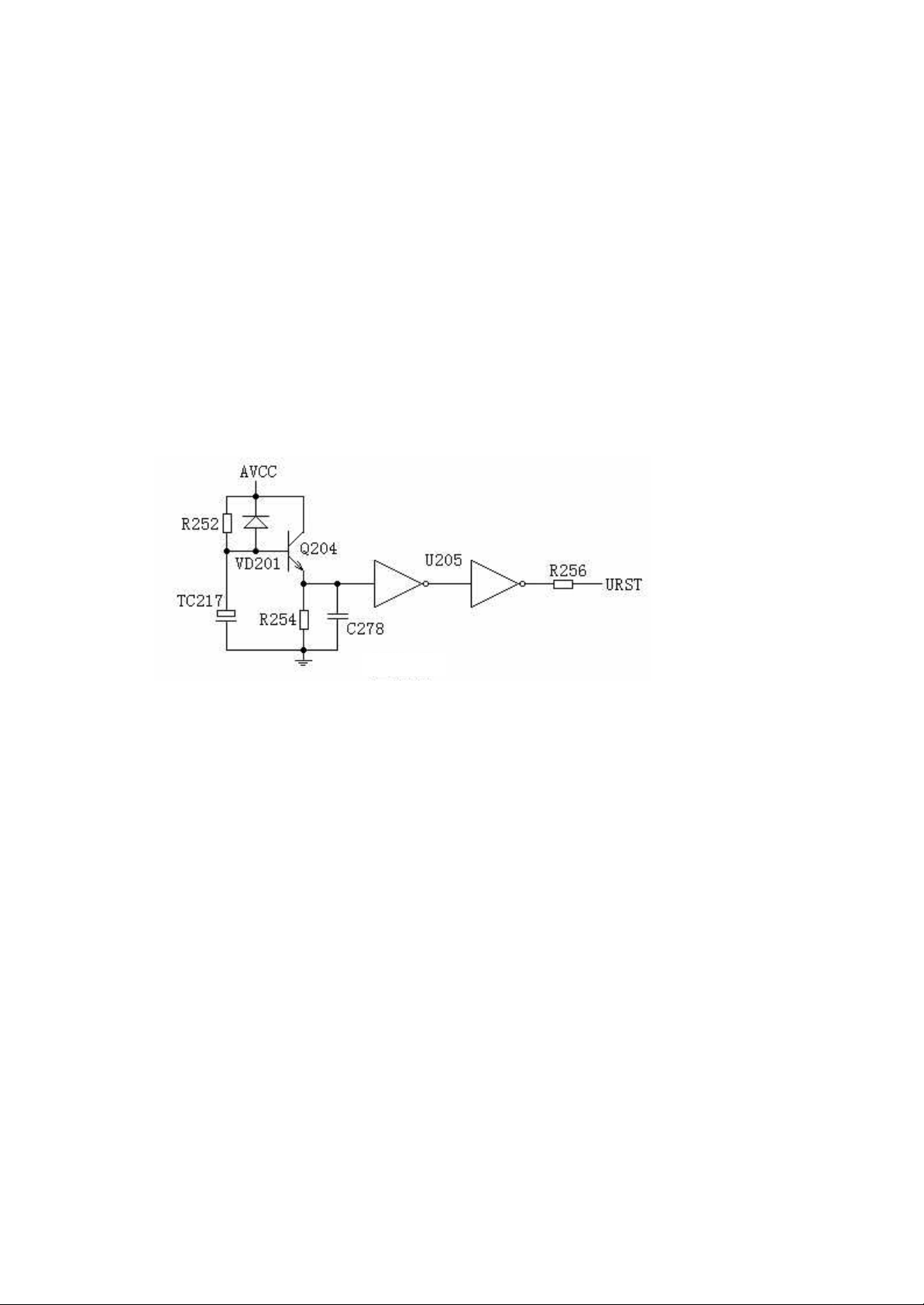
1. Reset circuit is as the Figure VI:
Figure VI
The reset circuit of the player consists of triode Q204 9014, reset capacitor TC 217 100uF/16V and
phase inverter U205 HCU04. In starting up, as the terminal voltage of capacitor cannot be changed
suddenly, the basic of Q204 is in low power level. After the cut-off of Q204, its emission polar is
in low power level, after secondary phase inversion by U205 and regulation, the low power level
reset signal is outputted to the Pin 110 of MT1389 to reset MT 1389.
When the recharging of TC217 is finished, the base of Q204 will be in high power level, Q204 will
be conducted, and the emission polar is in high power level. After the secondary phase inversion
and regulation by U205, a high power level is outputted and added to the Pin 110 of MT1389 to
maintain high power level during its normal operation.
2. Clock circuit
The crystal oscillator of X201 27MHz, C275/27PF, C276/27PF and phase inverter HCU04 form
into clock oscillation circuit, and the clock signals generated are added to the pins 229 and 228 of
MT1389 through R244 and 4248 to provide operating clock for MT1389.
3. Data communication circuit
The data communication circuit of the player consists of decoding chip MT1389, SDRAM,
AE45164016 and FLASH ROM 29LV160BE, as the Figure VII:
MT1389 is a piece of super large integrated circuit, with the operation voltage of +3.3V and +1.8V.
Its functions include: RF small signal preposition processing, digital servo, digital signal
processing and accomplishing MPEG decoding and video coding. The built-in MCU of MT1389 is
Page 10
also the system control circuit of the whole player.
39 38 37 18 17 19 16 20 21
77
26 28 11 15 47 79 66 VD
AE45164016 is a piece of 4M*16bit large capacity SDRAM, with the operation voltage of +3.3 V.
In DV971, the 6ns module is adopted, with high speed and the maximum operation frequency up
to 166MHz. Its main function is for operation buffer storage of decoding chip MT1389 to store the
audio and video data stream in decoding.
29LV160BE is a piece of 16Mbit FLASH ROM, with the operation voltage of +3.3V, mainly for
storing the user’s information including OSD character information, operational microcode and
LOGO in start-up.
RY/BY
29LV160BE
BYTE
GND
A0—A21
AD0—AD7
DCE
DRD
DWR
Figure VII
MT1389
DMA0—DMA11
DQ0—DQ15
113
137
156
157
140
139
142
138
145
143
AE45164016
DQML
15
DQMH
CLK
CKE
RAS
CAS
CS
WE
BA1
BA0
II. Audio and Video Output Circuit
1. Video output circuit
DK1010S can not only output three types of alternating-line video signal (including CVBS
composite video, S terminal Y-C signal and Y/Cb/Cr color difference signal), but also output two
types of progressive line video signal (including Y/Pb/Pr progressive line color difference signal
and VGA progressive line signal).
The decoding chip MT1389 has built-in video encoding circuit for direct output of analogue
composite video signal CVBS, S terminal, color difference signal and VGA signal.
The CVBS composite video signal is outputted from the Pin 198 of MT1389, the S terminal signal
Y-C is outputted from the pins 194 and 196 of MT1389, the color difference signal and the R-B-G
signal of VGA port is outputted from the pins 203, 202 and 200 of MT1389, the row and field
synchronization signals of VGA port are outputted from the pins 207 and 205 of MT1389
respectively.
To mention specifically, the alternating-line color difference signal, the progressive line color
difference signal and progressive line R-B-G signal are outputted from the same pin, therefore the
signal output shall be selected according to the ports of TV, otherwise there will be only sound but
without picture display.
2. Audio output circuit
Audio signals processed by MT1389 output 5-track data signals through pin 217, pin 218 and pin
219 and 5-channel clock signals through pin 214 and pin 215. These signals after passing through
Page 11

IC 74HCT125 are transmitted to audio signal processing IC TAS5508 to be processed (specific IC
data please refer to Attachment), then 10 groups of PWM signals are output, six of which are
transmitted to power amplifying parts, two of which to headphone output and two of which to
auxiliary channel output.
Six groups of signals transmitted to power amplifying IC are processed by surrounding and super
DBB sharing an N13 IC TAS5508, and by main sound channel and center sharing an N14 IC
TAS5508. Signals are amplified here, for they are digital high frequency signals, they have high
efficiency; meanwhile power IC has low colorific value. Amplified signals are still digital signals,
in order that they can be output through loudspeaker, amplified digital signals still have to be
processed before outputting.
For PWM signals containing audio signals, since high frequency signals have high frequency and
are beyond audibility range of human ears, we can ignore impacts of high frequency signals and
reduce low frequency audio signals only during processing.
TAS5508 is an 8-channel pulse width modulated high performance IC, and applicable in
processing most digital audio signals. Between 20Hz and 20KHz, it has excellent noise factor and
dynamic range. It has following features:
1、 Automatically control clock speed and digital sampling speed;
2、 8 groups of audio input channels;
3、 8 groups of PWM output can be changed into 6-channel stereo line output or 8-channel
line output;
4、 Line output is a different input open loop amplifier driven by a group of PWM signals.
IC TA S5112 is a high performance audio power amplifier. Bridging with 6O loading, each channel
can output 50W. It has 95DB dynamic range, low distortion degree and low rate of heat generation
with power efficiency up to 90%. It also has functions of low-voltage protection, high-temperature
protection, overflow protection, etc. At the same time, it has built-in driving power adjustment gate
circuit. It is applicable in family video, DVD receiver, mini music center, etc. Detailed IC
introduction see Attachment.
When in normal disc reading, digital signals and c lock signals from 1389 are transmitted to pin 26
to pin 31 of IC TAS5508 through IC 74HCT125 gating. If no headphone is inserted, PH-SEL is of
high level, as well as when MUTE is normal. And pin 37 of TAS5508 is also of high level. All data
lines and clock lines can be detected by oscilloscope. One group of signals from 5508 is
transmitted to N8 and N9, then output through auxiliary channel. Another group is transmitted to
headphone; other PWM signals are transmitted to amplifying parts of amplifier.
When headphone is inserted, PH-SEL signal is forcibly shorted to earth, and turns to low level,
meanwhile amplifier is muted.
This amplifier has functions of radio reception, auxiliary channel output and karaoke. All external
inputs after N3 CD4052 gating and N7 CS5340 analog-to-digital conversion are transmitted to
MT1389. Rear processing and output is the same as the signal output flow in normal disc reading.
When in disc reading, system defaults to gate karaoke input, therefore you can open karaoke when
playing disc. This amplifier also has automatic accompaniment function, when playing VCD,
system detects external input and automatically screen to human sound signal in the disc, while
only saves sound accompaniment.
DK1010S has the function of radio reception, and can also receive RDS signal. The radio head
control lines CE, DI, CL and DO are controlled by 28 array lines connecting to MT1389 control.
Page 12

When any of the controlling lines is in abnormality, the radio reception will be in malfunction. The
RDS signal received by radio head will be delivered to the dedicated IC SAA6588 for processing.
Chapter IV Operating Principle of Power Board
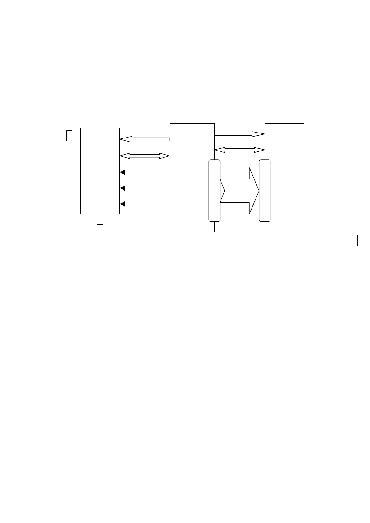
I. Block Diagram
This amplifier has two groups of power supply; one is of low voltage for decoding board and low
power ICS, the other is of higher voltage for power amplifying IC. But their design principles, we
only draw one functional block diagram of them:
II. Introduction of Circuit Principle
220V alternating current is loaded on D501-D504 integrated bridging rectification circuit through
power plug, fuse tube, voltage dependent resistor R501 and common mode rejection BC501 and
L501. Diode adopts IN4007 which ahs better PPR and higher withstand voltage value than IN4001.
Output 311V direct current after being bridging rectified is loaded on two transformers through
TC501 filtering and transmitted to DRAIN control pins of switch modules U501 and U502.
Service voltage of power on IC after being directly rectified and filtered is divided by resistors to
serve IC. Diode D508, capacitor C516 and resistor R516 form absorption circuit to provide
discharge circuit of reverse electromotive force for 1-4 coils of transformers. Pin FB controlling IC
is feedback control pin, so you should decide on/off time of pulse width according to current
intensity on it to ensure stability of output voltage.
There are 5 branch circuits coupled to sub -grade through transformer.
1. Voltage output from pin 11 and pin 13 of transformer T501 outputs a group of +28V voltage
for power amplifying IC after being rectified and filtered.
2. Voltage output from pin 16 of transformer T501 outputs a group of +12V voltage after being
rectified and filtered. +12V voltage is stabilized into a group of +5V voltage by IC LM7805.
3. Voltage output from pin 14 of transformer T501 outputs +5V voltage and provide voltage for
one end of photo-electric coupler U502 after being rectified and filtered.
4. Voltage output from pin 12 of transformer T501 outputs +3.3V voltage and provide a group of
stable voltage for CPU after being rect ified and filtered.
5. Voltage output from pin 9 of transformer T501 outputs a group of 21V voltage for displaying
driving IC after being rectified and filtered. Clamp ZD501 of -21V provide heater voltage for
panel display screen. Grounding direct voltage of FL+ and FL- is about -16V.
Operating principles of two groups of switch power are the same, therefore we will only analyze
the group providing +3.3V voltage for CPU here:
Feedback sampling of this group comes from 3.3V and supplies for photocupler HS817 through
D516 and R506. At the same time, it is divided through R508 and R509 for reference voltage pin R
of 2.5V comparator. When 3.3V becomes higher, pin KA of comparator is on; and the voltage is
transmitted to pin 4 of switch IC 5L0380R after photoelectr ic coupling through HS817 to reduce
on time of internal switch tube. And thus it reduces transformer coupling and decreases output of
3.3V voltage to achieve automatic adjustment and control, and vice verse.
It has to be noted that in this switching power reference voltage comparator IC of two groups of
switching power are different. For voltage of the group supplying power for amplifier is higher, it
adopts LM431 which has better performance and higher withstand voltage. And voltage of the
Page 13

group supplying power for 3.3V is lower, it adopts 17431. For two ICs are different, you should
VFD401 is a vacuum fluorescence screen, and its biggest feature is its high brightness.
IC 079
3
pay special attention to distinguish them from each other. They cannot be used mixing.
Chapter 5: Panel control and VFD display circuit
The panel mainly consists of VFD screen, driver IC0793, remote receptor HS0038A2 and
button and indicator display circuit, mainly for accomplishing man-player dialogue and display of
operation status.
The structural drawing is as follows:
Keystroke
VFD
display
control
U401
VFDST
VFDCK
VFDAT
U201
MT1389
Panel indicator control
Remote
receiving
Figure XI
MT1389 will control the U401 IC 0793 to display the operation status of the player through the
VFDST status, VFDCK clock and VFDAT data, under the control of CPU built in MT1389,
receive the user control commands sent by UPD16312, and control the controlled circuit of the
player to li mit the player to operate in specified status.
When the user operates the panel buttons, the control command is sent to the IC 0793 through
keyboard-scanning circuit, and through internal decoding drive, the IC 0793 outputs the control
data from the pins 5 and 6 (VFDAT) to the built-in CPU of MT1389, which will realize the control
on the controlled circuit, and control the VFD through IC 0793.
Its operation principle is similar to the kinescope of TV. The pins 1, 2, 34 and 35 are for filament
power supply; the pins 27-32 are GRID poles, each GRID has 16 different characters of display;
the pins 4-19 are SEG poles, and the CPU control the SEG poles through its control on IC 0793,
and display the characters of corresponding operation status on the screen.
The remote reception circuit mainly consists of remote receptors HS0038A2, of which the pin 1 is
for grounding, the pin 2 for power supply, the pin 3 for output of reception signal, and they are all
connected directly to the CPU in MT1389 to control the corresponding circuit.
This player has headphone output function. A pin in the headphone directly connects to TAS5508. When the
headphone is inserted, detection line H-DET grounds and turns into low level. When pin 12 of TAS5508 turns
Page 14

into low level, parts of output of amplifier are muted. When in normal condition, this detection pin is of high
level around 3.3V.
Troubleshooting
I. Voltage on key points of DK1010S
Demoding circuit:
Reset:
1. U205 (HCU04): 8 pins, around 5V;
2. MT1389: 110 pins, around 5V;
3. FLAHS ROM: 12 pins, around 5V
Clock:
27MHZ crystal oscillator two ends: Around 0.77V.
I2C bus SDA: 3.3V
I2C bus SCL 3.3V
Servo circuit:
LD01: 3.3V;LD02:3.3V
V301 and V302 electron collector LD voltage: 2.3V
BA5954 pin 4 base voltage: 1.4V
BA5954 pins 15 and 16 tracking drive output: Around 2.5V
BA5954 pins 17 and 18 feed drive output: Around 2.5V
BA5954 pins 13 and 14 focus drive signal output: Around 2.5V
BA5954 pins 11 and 12 main shaft drive output: Around 2.5V
BA5954 pin 1 focus control signal input: 1.4V
BA5954 pin 5 main shaft control signal input: 1.4V
BA5954 pin 26 tracking control signal input: 1.4V
BA5954 pin 23 feed control signal input: 1.4V
Amplifier circuit:
TAS5508 pin 9 power supply pin 3.3V
TAS5112 32、33、40、41、44、45、52、53, 28V。\
Page 15

No
display
Check if power supply of MT1389
Check the voltage of power board,
is
, C275,
is
Check if the reset circuit which is
Q204 etc.
SDA, SCL 3.3V
short
R260
f SDRAM CLK, CS, RAS, CAS,
f FLASH ROM, URST, DCE,
Check if the connection between
II. Troubleshooting of main troubles
picture, no sound, no VFD
3.3V, 1.8V is right?
YES
If the clock signal output XO
and XI is right?
YES
Check if reset signal URST#
NO
in 5V high level?
YES
Check if I2C bus,
voltage is right?
NO
NO
and check if the decoding board
short circuit to the grounding.
Check if clock oscillating circuit
27M crystal oscillator
C276, R224, R248 are damaged?
comprised by HCU04 and
is in working order?
Check if the AT24C16, CS4360,
MT1389 SDA and SCL are
circuit to grounding, if R259 and
are in working order?
Check i
WE communication signals are right?
MT1389, FLASH, SDRAM is right?
Check i
DRD, DWR signals are right?
Check if the MT1389, SDRAM and
FLASH are damaged?
Page 16

laser
feed control
23 is
17,18
er
Check if laser head
control
voltage output of
re
coil and its
Check if BA5854 and 5V power
Do not read disc
NO
Check if the
head has feed action.
Check if the
input of BA5954 Pin
1.4V?
YES
Check if the
connection from
BA5954 to MT1389
is open circuit ?
YES
YES
has focus action?
YES
YES
Check if the
BA5954 pin 13 and 14 a
Check if BA5954 pin
have 2.5V voltage output?
NO
Check if BA5854 and the pow
supply 5V are in working order ?
NO
Check if BA5954 pin 1
has focus
voltage input of 1.4V.
Check focus
connection.
2.5V?
Check feed motor
and its connection.
Check if the
connection from
BA5954 to MT1389
is open circuit ?
YES NO
supply are in working order ?
Page 17

Check MT1389 and its
301 and V302
electron collector voltage is
Check if the laser head
and its array line are
5
Check if the connection from
en
main shaft
11
Check if MT1389
peripheral
Check if BA5854 and 5V power
Check if there is
NO
laser coming out
from laser head?
Check if the signal
voltage of LD01, LD02
is 3.2V?
YES
Check if V
connection.
YES YES
Check if the
NO
main shaft
rotates?
YES
YES
YES
2.3V?
Check if the control
voltage of BA5954 pin
main shaft is 1.4V?
Check if BA5954 pin
and 12 output is 2.5V?
right?
BA5954 to MT1389 is op
circuit?
Check if BA5954 or
motor is damaged?
NO
and its
circuit is right?
supply are in working order?
Page 18

Attachment :Brief Introduction to IC Pins
I. MT1389
MT1389 adopts the LQFP 256 pin packaging and 3.3V/1.8V double voltage operation mode. It is a
piece of large-scale CD-ROM and DVD-ROM preposition processing CMOS integrated circuit
with excellent performance, and a single chip dedicated to CD/VCD/DVD player. It contains
focusing servo error amplification, tracking servo error amplification and RF level output servo
control, including the following main functions:
RF small signal preposition processing, mainly for carrying our corresponding processing and
amplification on the RF signals transmitted from the light head part, adjusting the laser output
power automatically, and identifying the VCD disc and DVD disc.
Digital servo processing can generate focusing, tracking, feed and main shaft servo control signals;
digital signal processing, accomplishing the EFM/EFM + demodulating of RF signals.
MPEG-1/MPEG-2/MPEG4/JPEG Video decoding chip, which can not only realize the decoding of
VCD and DVD, but also realize MPEG 4 network video decoding, being compatible to “network
movie” disc, and decipher JPED pictures to realize the function of digital photo album play.
On audio aspect, it can not only realize AC-3/DTS double decoding, decipher MP3, and is
also compatible to DVD-Audio decoding to achieve high-resolution sound restoration in 1000
times higher than CD.
By utilizing the 8032 microprocessor with built-in chip, MT1369E can also realize the system
control function of player, which simplifies the circuit design substantially.
The pin functions of MT1389 are as the following table:
Pin Name Function
1 AGND Analogue grounding
2 DVDA
3 DVDB
4 DVDC
5 DVDD
DVD-RF high-frequency AC coupling
signal A
DVD-RF high-frequency AC coupling
signal B
DVD-RF high-frequency AC coupling
signal C
DVD-RF high-frequency AC coupling
signal D
6 DVDRFIP
7 DVDRFIN
8 MA
DVD-RF high-frequency AC coupling
signal RFIP input
DVD-RF high-frequency AC coupling
signal RFIN input
DVD-RAM main light beam RF DC
signal input A
Page 19

9 MB
DVD-RAM main light beam RF DC
signal input B
10 MC
11 MD
12 SA
13 SB
14 SC
15 SD
16 CDFON CD focusing error phase inversion input
17 CDFOP CD focusing error phase input
18 TNI
DVD-RAM main light beam RF DC
signal input C
DVD-RAM main light beam RF DC
signal input D
DVD-RAM auxiliary light beam RF DC
signal input A
DVD-RAM auxiliary light beam RF DC
signal input B
DVD-RAM auxiliary light beam RF DC
signal input C
DVD-RAM auxiliary light beam RF DC
signal input D
3 light beam auxiliary PD signal phase
inversion input
19 TPI
20 MDI1 Laser power monitoring input 1
21 MDI2 Laser power monitoring input 2
22 LDO2 Laser power monitoring output 2
23 LDO1 Laser power monitoring output 1
24 SVDD3 Servo 3.3V power supply
25 CSO/RFOP
26 RFLVL/RFON
27 SGND Servo grounding
28 V2REFO Reference voltage 2.8V
29 V20 Reference voltage 2.0V
4 light beam auxiliary PD signal phase
input
Main servo signal output/RF phase
output
RF level output/RF phase inversion
output
30 VREFO Reference voltage 1.4V
31 FEO Focusing error signal output
32 TEO Tracking error signal output
Page 20

33 TEZISLV Tracking zero crossover error input
34 OP_OUT Sensing signal amplification output
35 OP_INN Sensing signal phase inversion input
36 OP_INP Sensing signal non-inverting input
37 DMO Main shaft control signal output
38 FMO Feed control signal output
39 TROPEN PWM Tray Open signal output
40 PWMOUT1/ADIN9
41 TRO Tracking control signal output
42 FOO Focusing control signal output
43 USB_VSS USB grounding
44 USBP USB data
45 USBM USB data
46 USB_VDD3 USB 3.3V power supply
47 FG/ADIN8
48 TDI/ADIN4
49 TMS/ADIN5
First-route pulse width demodulating
signal output/AD universal input
Motor sensing signal input/AD universal
input
Open position detecting signal input/AD
universal input
Close position detecting signal input/AD
universal input
50 TCK/ADIN6
51 TDO/ADIN7
52、97、122、
152、173、221
53-58 IOA2-7 Micro-controller address bit 2-7
59 HIGHA0 Micro-controller address bit 0
60、61 IOA18-19 Micro-controller address 18-19
62、85、94、116、
119、134、144、
148、161、163、
175、216、223
63 APLLCAP
DVDD18 Digital 1.8V power supply
DVSS Digital grounding
BA5954 enabling signal output/AD
universal output
Tray close signal output/AD universal
input
Analogue phase lock loop external
Page 21

capacitor
64 APLLVSS Analogue phase lock loop grounding
65 APLLVDD3 Analogue phase lock 3.3V power supply
66 IOWR FLASH read control signal
67-72 HIGHA3-7 Micro-controller address bit 3-7
73、80、108、
127、141、155、
167、182、204、
212
74、75 HIGHA1-2 Micro-controller address bit 1-2
76 IOA20 Micro-controller address bit 20
77 IOCS FLASH chip selection
78 IOA1 Micro-controller address bit 1
79 IOOE FLASH output enabling
DVDD3 Digital 3.3V power supply
81-84 AD0-3 Micro-controller address/data bit 0-3
86-88 AD4-6 Micro-controller address/data bit 4-6
89 IOA21/ADIN0
90 ALE Micro-controller address enabling
91 AD7 Micro-controller address/data bit 7
92 A17 FLASH address bit 17
93 IOA0 Micro-controller address bit 0
95 UWR Micro-processor reading operation
96 URD Micro-processor reading operation
98 UP1_2-1_7 Micro-processor port
104 UP3_0 Micro-processor port
105 UP3_1 Micro-processor port
Micro-controller address bit 21/AD
universal input
106 UP3_4 Micro-processor port
107 UP3_5 Micro-processor port
109 ICE
110 PRST Reset input
111 IR Remote control signal input
Micro-processor correction mode
enabling
Page 22

112 INT0 Micro-processor interruption 0
113 DQM0 DRAM input output shielding signal
114 DQS0 DRAM input output shielding signal
115 RD7 DRAM data
117-118 RD5-6 DRAM data
120-121 RD3-4 DRAM data
123-125 RD0-2 DRAM data
126 RD15 DRAM data
128-133 RD9-14 DRAM data
135 RD8 DRAM data
136 DQS1 DRAM input output shielding signal
137 DQM1 DRAM input output shielding signal
138 RWE DRAM writing enabling
139 CAS DRAM column address selection
140 RAS DRAM row address selection
142 RCS DRAM chip selection
143 BA0 DRAM section address 0
145 BA1 DRAM section address 1
146 RA10 DRAM address
147 RA0 DRAM address
149 RA1-3 DRAM address
153 RVREF/ADIN3 Reference voltage/AD universal input
154 RCLKB DRAM clock
156 RCLK DRAM clock
157 CKE DRAM clock enabling
158 RA11 DRAM address
159-160 RA8-9 DRAM address
162 RA7 DRAM address
164 RA4-6 DRAM address
168 RD13/ASDATA5 DRAM data/audio series data
169 RD27-30 DRAM data
Page 23

174 RD26 DRAM data
176-177 RD24-25 DRAM data
178-179 DQM2-3 DRAM I/O shielding signal
180-181 RD22-23 DRAM data
183-188 RD16-21 DRAM data
189 DACVDDC D/A conversion 3.3V power supply
190 VREF Reference voltage
191 FS
192 YUV0/CIN
193 DACVSSC D/A conversion grounding
194 YUV1/Y
195 DACVDDB D/A conversion 3.3V power supply
196 YUV2/C
197 DACVSSB D/A conversion grounding
198 YUV3/CVBS
199 DACVDDA D/A conversion 3.3V power supply
200 YUV4/G
201 DACVSSA D/A conversion grounding
202 TUV5/B
203 YUV6/R
Video signal YUV1 output/Y signal
output
Video signal YUV2 output/C signal
output
Video signal YUV3 output/CVBS signal
output
Video signal YUV4 output/G signal
output
Video signal YUV5 output/B signal
output
Video signal YUV6 output/R signal
output
205 VSYNC/ADIN1
206 YUV7/ASDATA5
207 HSYNC/ADIN2
208 SPMCLK
209 SPDATA
Field synchronization signal output/AD
universal input
Video signal YUV7 output/audio series
data
Row synchronization output/AD
universal input
Page 24

210 SPLRCK
211 SPBCK/ASDATA5
213 ALRCK Audio left and right sound channel clock
214 ABCK Audio bit clock
215 ACLK Audio DAC external clock
217-220 ASDATA0-3 Audio series data
222 ASDATA4 Audio series data
224 MC_DATA Microphone digital audio input
225 SPDIF Digital audio signal output
226 RFGND18 RF signal grounding
227 RFVDD18 RF signal 1.8V power supply
228 XTALO Clock output
229 XTALI Clock input
230 JITFO RF small signal output
231 JITFN
232 PLLVSS Phase lock loop grounding
233 IDACEXLP
234 PLLVDD3 Phase lock loop 3.3V power supply
235 LPFON Amplifier loop wave filtration output
236 LPFIP Amplifier loop wave filtration input
237 LPFIN Amplifier loop wave filtration input
238 LPFOP Amplifier loop wave filtration output
239 ADCVDD3 A/D conversion 3.3V power supply
240 S_VCM
241 ADCVSS A/D conversion grounding
242 S_VREFP
RF small signal phase inversion and
amplification input
243 S_VREFN
244 RFVDD3 RF 3.3V power supply
245 RFRPDC DC RF error signal input
246 RFRPAC AC RF error signal input
247 HRFZC
High-frequency RF signal zero
Page 25

crossover checking
248 CRTPLP
249 RFGND RF grounding
250 CEQP
251 CEQN
252 OSP
253 OSN
254 RFGC
255 IREF Reference current
256 AVDD3 Analogue 3.3V power supply
Ⅱ.BA5954
BA5954 is a piece of servo drive single-piece integrated circuit, with built-in 4-channel BTL drive
circuit. It can receive directly the PWM control signal output by digital servo IC, and with internal
wave filter and drive amplifier, it pushes the execution part in the servo mechanism to accomplish
the focusing, tracking, feed and main shaft drives. BA5954 adopts the packaging of 28 pins.
Note: The 28 pins of BA5954 are for outputting effective control signal, which is provided by the
50 pins of MT1389. When the signal is in high power level, BA5954 output is in validity, while the
signal is in low power level, BA5954 will not be activated, and its output ports are in the state of
cutoff.
The functions of pins of BA5954 are as the following table:
Pin Name Function
1 VINFC Focusing control signal input
2 CF1 External feedback loop
3 CF2 External feedback loop
4 VINSL+ Forward control input, connected to the reference voltage
5 VINSL- Main shaft control signal input
6 VOSL External feedback resistance
7 VINFFC Focusing feedback signal input
8 VCC 5V power supply
9 PVCC1 5V power supply
10 PGND Grounding
Page 26

11 VOSL- Main shaft drive inverse voltage output
12 VO2+ Main shaft forward voltage output
13 VOFC- Focusing drive inverse voltage output
14 VOSC+ Focusing drive forward voltage output
15 VOTK+ Tracking drive forward voltage output
16 VOTK- Tracking drive inverse voltage output
17 VOLD+ Feed drive forward voltage output
18 VOLD- Feed drive inverse voltage output
19 PGND Grounding
20 VINFTK Tracking feedback signal input
21 PVCC2 5V voltage
22 PREGND Grounding
23 VINLD Feed control signal input
24 CTK2 External feedback loop
25 CTK1 External feedback loop
26 VINTK Tracking control signal input
27 BIAS 1.4 reference voltage input
28 STBY Enabling control signal
III. 29LV160BE
29LV160BE is a type of 16Mbit FLASH memory manufactured via 0.23um technology, with 16
byte width DQ0-DQ15, memory capacity of 16M bit, operation voltage of 3.3V, and packaging
method of 48 pins TSOP. The specific operation mode is as the following table:
DQ8~DQ15
Operation
status
CE OE WE RESET A0~A19 DQ0~QD7
BYTE:high
level
BYTE: Low
level
Read L L H H Ain Dout Dout High resistance
Write L H L H Ain Din Din High resistance
Waiting H × × H ×
Output
forbidden
L H H H ×
high
resistance
High
resistance
high resistance high resistance
High resistance High resistance
Page 27

Reset × × × L ×
High
resistance
High resistance High resistance
The functions of pins of 29LV160BE are as the following table:
Pin Name Function
15 RY/BY Ready/system is busy
1~9、16~25 、48 A0~A19 20-byte address bus
26 CE Chip enabling
27、46 VSS Grounding
28 OE Output enabling
29~36、38~44 DQ0~DQ14 15-byte data bus
37 VCC 5V power supply
45 DQ15/A-1
47 BYTE
11 WE Write enabling
12 RESET Reset, valid in low level
10、13、14 NC Neutral pin
Character extension mode as the data line; byte expansion
mode as the address line
Adopting 8-byte (in low level) or 16-byte output mode (in
high level)
IV. AE45164016
AE45164016 is a type of 64Mb (4Banks×1M×16bit) CMOS synchronization DRAM, featured
with large memory and high speed. Its operation power voltage is 3.0V~3.6V, and it is packaged in
54-pin TSOP.
The functions of pins of AE45164016 are as the following table:
Pin Name Function
1、14、27 VDD +3.3V power supply
2、4、5、7、8、10、11、
13、42、44、45、47、48、
50、51、53
3、9、43、49 VDDQ +3.3V power supply
6、12、46、52 VSSQ Grounding
28、41、54 VSS Grounding
DQ[0~15]
16-byte data bus
Page 28

15 LDQM Data I/O shielding signal
16 WE Write control signal
17 CAS Column address gate signal
18 RAS Row address gate signal
19 CS Chip selection signal
20 SD-BS0 Section address 0 gate signal
21 SD-BS1 Section address 1 gate signal
22~26、29~35 MA[0~11]
36、40 NC Neutral pin
37 CKE Clock enabling signal
38 CLK System clock input
39 UDQM Data I/O shielding signal
12-byte address bus
V. Pin Functions of TAS5508
TAS5508 is a high performance audio signal processing IC provided by TI. It has 8-channel PWM
processing function, perfect protective functions, low distortion degree and excellent dynamic
characteristics.
1 VRA_PLL Provide 1.8V reference voltage for PLL
2 PLL_FLT_RET PLL external filtering circuit
3 PLL_FLTM PLL inverted input pin
4 PLL_FLTP PLL non-inverted output pin
5 AVSS Analog grounding
6 AVSS Analog grounding
7 VRD_PLL Provide 1.8V reference voltage for PLL
8 AVSS_PLL PLL analog grounding
9
10 VBGAP Provide 1.2 V reference voltage
11 RESET System reset signal, valid in low level
12 HP_SEL Microphone input/output selection
13 PDN Switch-off voltage, valid in low level
14 MUTE Software muting control, valid in low
15 DVDD 3.3V digital power supply
16 DVSS Digital grounding pin
17 VR_DPLL Provide 1.8V reference voltage for PLL
18 OSC_CAP Oscillation capacitance
19 XTL_OUT Crystal oscillation output pin
20 XTL_IN Crystal oscillation input pin
21 RESERVED Connect to digital grounding
22 TBASE_SEL Connect to digital grounding
PLL provides 3.3V voltage
level
Page 29

23 RESERVED Connect to digital grounding
Output PWM signal is displayed normally,
24 SDA Digital signal
25 SCL Clock signal
26 LRCLK RF channel clock signal
27 SCLK Audio clock signal
28 SDIN4 Audio data input pin
29 SDIN3 Audio data input pin
30 SDIN2 Audio data input pin
31 SDIN1 Audio data input pin
32 PSVC Control PWM signal output
33 VR_DIG 1.8V reference voltage of digital core
34 DVSS Digital grounding
35 DVSS Digital grounding
36 DVDD 3.3Vdigital service voltage
37 BKND_ERR Logic error control pin, valid in low
level
38 DVSS Digital grounding
39 VALID
valid in high level
40 PWM_M_1 PWM signal output 1
41 PWM_P_1 PWM signal output 1
42 PWM_M_2 PWM signal output 2
43 PWM_P_2 PWM signal output 2
44 PWM_M_3 PWM signal output 3
45 PWM_P_3 PWM signal output 3
46 PWM_M_4 PWM signal output 4
47 PWM_P_4 PWM signal output 4
48 VR_PWM 1.8V reference voltage of PWM core
49 PWM_M_7 PWM signal output 7
50 PWM_P_7 PWM signal output 7
51 PWM_M_8 PWM signal output 8
52 PWM_P_8 PWM signal output 8
53 DVSS_PWM Digital grounding for PWM signal
54 DVDD_PWM 3.3V voltage for PWM signal
55 PWM_M_5 PWM signal output 5
56 PWM_P_5 PWM signal output 5
57 PWM_M_6 PWM signal output 6
58 PWM_P_6 PWM signal output 6
59 PWM_HPML Headphone output PWM left channel
60 PWM_HPPL Headphone output PWM left channel
61 PWM_HPMR Headphone output PWM right channel
62 PWM_HPPR Headphone output PWM right channel
63 MCLK 3.3V clock input
64 RESERVED Connect to digital grounding
Page 30

IV. IC TAS5112
IC TAS5112 is an audio power amplifier of high performance made by TI. Bridging with 6O
loading, each channel can output 50W. It has 95DB dynamic range, low distortion degree and low
rate of heat generation with power efficiency up to 90%. It also has functions of low-voltage
protection, high-temperature protection, overflow protection, etc. At the same time, it has built-in
driving power adjustment gate circuit. Basic functions of its pins are as shown in the following
table:
Pin Name Function
31 BST_A Auxiliary power
42 BST_B Auxiliary power
43 BST_C Auxiliary power
54 BST_D Auxiliary power
23 DGND Digital input output reference
16 DREG Digital service voltage adjustment
circuit
12 DREG_RTN Digital service voltage adjustment
circuit
25 DVDD Input output reference
1,2,22,24,28,
29,27,36,37,
48,49,56
3,26
30,55
15 M1(TST0) Mode selection
14 M2 Mode selection
13 M2 Mode selection
4 OTW Protective pin in the high
34,35
38,39
46,47
50,51
32,33 PVDD_A Service voltage of half bridge A
40,41 PVDD_B Service voltage of half bridge B
44,45 PVDD_C Service voltage of half bridge C
52,53 PVDD_D Service voltage of half bridge D
20 PWM_AM Inverted input pin
21 PWM_AP Non-inverted input pin
18 PWM_BM Inverted input pin
17 PWM_BP Non-inverted input pin
10 PWM_CM Inverted input pin
11 PWM_CP Non-inverted input pin
8 PWM_DM Inverted input pin
7 PWM_DP Non-inverted input pin
GND Grounding
GREG Driving voltage adjustment of gate
circuit
GVDD Digital voltage adjustment
temperature
OUT_A Output pin A
OUT_B Output pin B
OUT_C Output pin C
OUT_D Output pin D
Page 31

19 RESET_AB Reset signal , valid in low level
9 RESET_CD Reset signal , valid in low level
6 SD_AB Signal switch off control
5 SD_CD Signal switch off control
IIV. IC SE5532
IC SE5532 is an amplified IC with dual channels and low noise. Compared to most other amplified
ICs, it has lower noise, better output performance and power bandwidth. Its main features are:
small -signal bandwidth; its direct voltage gain can be up to 50000 and alternating voltage gain can
be up to 2200 under 10KHz; its power bandwidth can be up to 140KHz; relatively larger power
supply range; fast slewing rate. Basic functions of its pins are as shown in the following table:
Pin Name Function description
1 OUTPUT-A Output channel A
2 INVERTING INPUT -A Inverted input A
3 NON-INVERTING INPUT -A Non-inverted input A
4 V- Negative power supply
5 NON-INVERTING INPUT -B Non-inverted input B
6 INVERTING INPUT -B Inverted input B
7 OUTPUT-B Output channel B
8 V+ Positive power supply
IIIV、CS 534 0
CS 5340 is an IC of analog/digital conversion; it can be applied to sample, analog-to-digital
conversion and filter. During continuous input, its sampling frequency can be up to 200KHz. Its
main features are as follows:
24 bytes conversion; supported audio frequency can be up to 192KHz; under power of 5V, its
dynamic range can be up to 101DB; it has high pass filter to filter direct current. Functions of its
pins are as follows:
Pins Name Function description
1 M0 Mode selection
16 M1 Mode selection
2 MCLK Master clock signal
3 VL Logic voltage power supply
4 SDOUT Audio data output
5,14
6 VD Digital power
7 SCLK DRAM clock signal
8 LRCK RF clock signal
9 RST Reset signal
10 AINL Analog input
12 AINR Analog input
11 VQ Quiescent voltage
13 VA Analog power
15 FILT+ Reference voltage
GND Grounding
 Loading...