

Page 1

Four Port, PCI Bus
RS-232/422/485 Serial Card CE
with Send Data Control
3PCISD4A 3PCISD4B
Documentation Number 3PCISD4x-3903 (pn4324-r006)
This manual applies to models 3PCISD4A and 3PCISD4B. The “A” models are
equipped with 16550A UARTs which have 16 byte transmit and receive buffers. The
“B” models are equipped with 16850 UARTs with 128 byte transmit and receive
buffers. The model number of each card is printed on a sticker on the board.
This product designed and manufactured in Ottawa, Illinois USA
of domestic and imported parts by
International Headquarters
B&B Electronics Mfg. Co. Inc.
707 Dayton Road -- P.O. Box 1040 -- Ottawa, IL 61350 USA
Phone (815) 433-5100 -- General Fax (815) 433-5105
Home Page: www.bb-elec.com
Orders e-mail: orders@bb.elec.com
Technical Support e-mail: support@bb.elec.com
European Headquarters
B&B Electronics Ltd.
Westlink Commercial Park, Oranmore, Co. Galway, Ireland
Phone +353 91-792444 -- Fax +353 91-792445
Home Page: www.bb-europe.com
Orders e-mail: orders@bb-europe.com
Technical Support e-mail: support@bb-europe.com
2000 B&B Electronics -- Revised October 2003
-- Fax (815) 433-5109
-- Fax (815) 433-5104
2000 B&B Electronics . No part of this publication may be reproduced or transmitted in any form or by any
means, electronic or mechanical, including photography, recording, or any information storage and retrieval
system without written consent. Information in this manual is subject to change without notice, and does not
represent a commitment on the part of B&B Electronics.
B&B Electronics shall not be liable for incidental or consequential damages resulting from the furnishing,
performance, or use of this manual.
All brand names used in this manual are the registered trademarks of their respective owners. The use of
trademarks or other designations in this publication is for reference purposes only and does not constitute an
endorsement by the trademark holder.
Documentation Number 3PCISD4x-3903 Manual Cover Page
B&B Electronics Mfg Co – 707 Dayton Rd - PO Box 1040 - Ottawa IL 61350 - Ph 815-433-5100 - Fax 815-433-5104
B&B Electronics Ltd – Westlink Comm. Pk. – Oranmore, Galway, Ireland – Ph +353 91-792444 – Fax +353 91-792445
Page 2

TABLE OF CONTENTS
CHAPTER 1: GENERAL INFORMATION......................................1
NTRODUCTION .......................................................................................1
I
EATURES ...............................................................................................1
F
PECIFICATIONS ......................................................................................2
S
CHAPTER 2: SETUP .........................................................................5
I
NSPECTION.............................................................................................5
MODE.........................................................................................7
RS-232
Table 7: RS-232 Pinouts ...................................................................7
RS-422
MODE.........................................................................................7
RS-422/RS-485 Pinouts......................................................................8
MODE.........................................................................................8
RS-485
RS-485 Pinouts...................................................................................9
Explanation of RS-485 Operation ......................................................9
AND RS-485 TERMINATION......................................................10
RS-422
X BAUD RATE OPTION .......................................................................10
4
NSTALLING THE CARD..........................................................................11
I
CHAPTER 3: WINDOWS INSTALLATION ..................................13
WINDOWS
INDOWS 2000 ....................................................................................21
W
WINDOWS
CHAPTER 4: TROUBLESHOOTING ............................................33
95/98 ............................................................................... 12
NT 4.0 ..............................................................................27
APPENDIX A: DB9 SIGNAL CONNECTIONS .......................... A-1
APPENDIX B: JUMPER MODE TABLE .....................................B-1
APPENDIX C: 3PCISD4 I/O PINOUT ........................................ C-1
APPENDIX D: 3PCISD4 I/O SCHEMATIC ............................... D-1
APPENDIX E: RENAMING COM PORTS - WIN 95/98/ME ......E-1
APPENDIX F: DECLARATION OF CONFORMITY ..................F-1
Documentation Number 3PCISD4x-3903 Manual Table of Contents i
B&B Electronics Mfg Co – 707 Dayton Rd - PO Box 1040 - Ottawa IL 61350 - Ph 815-433-5100 - Fax 815-433-5104
B&B Electronics Ltd – Westlink Comm. Pk. – Oranmore, Galway, Ireland – Ph +353 91-792444 – Fax +353 91-792445
ii Table of Contents Documentation Number 3PCISD4x-3903 Manual
B&B Electronics Mfg Co – 707 Dayton Rd - PO Box 1040 - Ottawa IL 61350 - Ph 815-433-5100 - Fax 815-433-5104
B&B Electronics Ltd – Westlink Comm. Pk. – Oranmore, Galway, Ireland – Ph +353 91-792444 – Fax +353 91-792445
Page 3

Chapter 1: GENERAL INFORMATION
Introduction
• RS-485 Signal Lines: TD(A), TD(B), RD(A), RD(B) and Signal
Ground. (Data A & Data B lines when wired for 2-wire
operation.)
The B&B Electronics 3PCISD4x serial interface card is designed
for IBM compatibles with a PCI Bus. The PCI design is Plug and
Play compatible which allows the driver and Operating System to
select the IRQ and hardware addresses used by the card.
The 3PCISD4x card offers exceptional setup flexibility with a mix
of selectable operating modes. If you are writing your own
applications, be sure the communications routine used supports
Windows communication drivers and a wide range of COM ports.
Description
Each of the four ports can be independently configured for RS232, RS-422, or RS-485 data protocols. The 485-mode Send Data
Control feature transparently handles the enable and disable
functions of the RS-485 transceiver. Buffered, high speed UARTs
(16550A or 16850) make it ideal for high speed (modem) and
multitasking applications.
Features
• IBM compatible, PCI Version 2.1 bus
• Supports baud rates to 460.4 Kbaud with 4X clock option
enabled
• High speed 16 byte FIFO 16550A UARTs (Model 3PCISD4A),
128 byte FIFO 16850 UARTs (Model 3PCISD4B)
• RS-232/422/485 Mode Independently Configurable Fo r Each
Port
• RS-485 Automatic Send Data Control or RTS Control
• 2-wire or 4-wire RS-485 Operation (Half or Full Duplex)
• 120ΩTermination Select Jumpers for RS-422/RS-485 Networks
• RS-232 Mode Signal Lines: TD, RD, RTS, CTS, DSR, DTR,
DCD, RI and Signal Ground.
• 2 Channel RS-422 Signal Lines: TD(A), TD(B), RD(A), RD(B)
and Signal Ground
Specifications
Bus: PCI bus version 2.1
Slot: Requires 1 PCI slot
Dimensions: 11.2 x 4.2 in (28.4 x 10.7 cm)
I/O connection: One DB-37 female (DB-37F)
Cable: One DB-37 male to f our DB-9 male (included )
Replacement cable available, order model 37M9M
OS Supported: Windows 95, 98, 2000 and NT 4.0
Baud rates: 460,800 Baud Max - RS-232/422/485
UARTs: 16550A 16 byte TX and RX buffers (A model), or
16850 128 byte TX and RX buffers (B model)
Character length: 5, 6, 7, or 8 bits
Parity: Even, odd or none
Stop bits: 1, 1.5, or 2
RS-232 Control Lines Drivers/Receivers:
Device: 75185 Transceiver
High level output voltage: 6.0 V minimum
Low level output voltage: −6.0 V minimum
Output current limited to: ±10 mA
Input high threshold voltage: 1.5V
Input low threshold voltage: 0.75V
Device will withstand: ±30V
RS-232 Data Lines Drivers/Receivers:
Device: SP211H Transceiver
High level output voltage: 5.0 V minimum
Low level output voltage: −5.0 V minimum
Output current limited to: ±25 mA
Input high threshold voltage: 1.7V
Input low threshold voltage: 0.8V
Device will withstand: ±15V
Documentation Number 3PCISD4x-3903 Manual Chapter 1 1
B&B Electronics Mfg Co – 707 Dayton Rd - PO Box 1040 - Ottawa IL 61350 - Ph 815-433-5100 - Fax 815-433-5104
B&B Electronics Ltd – Westlink Comm. Pk. – Oranmore, Galway, Ireland – Ph +353 91-792444 – Fax +353 91-792445
2 Chapter 1 Documentation Number 3PCISD4x-3903 Manual
B&B Electronics Mfg Co – 707 Dayton Rd - PO Box 1040 - Ottawa IL 61350 - Ph 815-433-5100 - Fax 815-433-5104
B&B Electronics Ltd – Westlink Comm. Pk. – Oranmore, Galway, Ireland – Ph +353 91-792444 – Fax +353 91-792445
Page 4

RS-422/485 Driver/Receiver:
Device: 75ALS180 or MAX491
Differential driver output voltage: 1.5 - 6 V
Differential input high-threshold voltage: 0.2 V
Differential input low-threshold voltage: −0.2 V
Automatic RS-485 Driver Control Timing:
Driver is enabled when data is a logic “0” (start bit). Driver
remains enabled for one character transmission time (10 bits
of data at current baud rate). Each additional logic “0” resets
the timeout.
Termination: A 120Ω termination resistor is jumper selectable on
each 422/485 receiver.
Max Power Consumption: All ports loaded
+5V, 437 mA, 2.18W
+12V, 124 mA, 1.49W
-12V, 124 mA, 1.491W
Accessories:
Cable: One DB-37 Male to four DB-9 Male (included)
Replacement cable model number: 37M9M
Software: Driver Disk (3.5) for Windows 95/98/2000/NT 4.0
PCI/USB COM Port Utility Disk (3.5)
Manual: Instruction Manual (this booklet)
Documentation Number 3PCISD4x-3903 Manual Chapter 1 3
B&B Electronics Mfg Co – 707 Dayton Rd - PO Box 1040 - Ottawa IL 61350 - Ph 815-433-5100 - Fax 815-433-5104
B&B Electronics Ltd – Westlink Comm. Pk. – Oranmore, Galway, Ireland – Ph +353 91-792444 – Fax +353 91-792445
4 Chapter 1 Documentation Number 3PCISD4x-3903 Manual
B&B Electronics Mfg Co – 707 Dayton Rd - PO Box 1040 - Ottawa IL 61350 - Ph 815-433-5100 - Fax 815-433-5104
B&B Electronics Ltd – Westlink Comm. Pk. – Oranmore, Galway, Ireland – Ph +353 91-792444 – Fax +353 91-792445
Page 5
Chapter 2: SETUP
Inspection
Your 3PCISD4x serial card was tested for proper operation before
shipment. It should be in perfect mechanical and electrical condition
upon receipt.
The card is normally pre-configured for RS-232 operation on all
ports.
The data clock speed for all 4 ports is set by one jumper to x1
(normal) operation or to x4 operation.
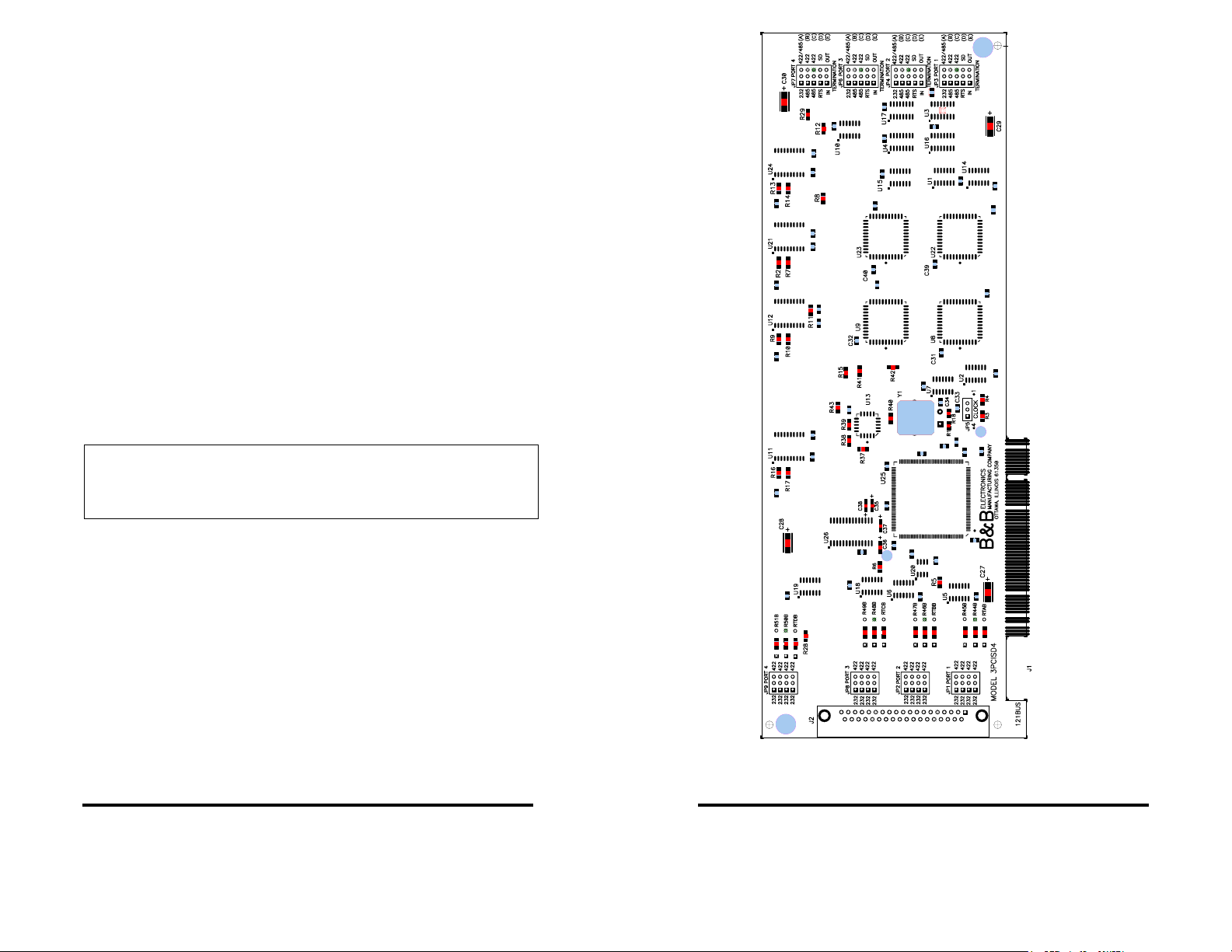
The operating mode of each port on the card is set using 9 jumpers:
5 jumpers select RS-232 operation or RS-422/485 operation, 2
select RS-422 or RS-485 operating modes for Receive and
Transmit, one sets the RS-485 mode driver control for Send Data or
RTS control, and the last selects 120 ohm termination for the RS422 or RS-485 Receive. Each of the 4 ports is configured in a
similar fashion.
Refer to Jumper Mode Tables, Appendix B.
CAUTION: ELECTROSTATIC SE NSITIVE DEVICE
Use ESD precautions for safe handling.
Before removing the card from the anti-static protective packaging:
• Discharge any static electricity buildup on your body by touching
a large grounded metal surface or the metal chassis on
equipment connected to earth ground by a 3-wire power cord.
• Avoid touching the gold connectors or other parts on the card
except as necessary to set the configuration jumpers for each
port. After setting the jumpers, ground yourself to the computer
chassis before and while inserting the card.
• Remove AC power from the computer and unplug the power
cord before inserting the card.
• Retain the ESD bag for handling the card. Save the packaging
for storage or shipping.
Documentation Number 3PCISD4x-3903 Manual Chapter 2 5
B&B Electronics Mfg Co – 707 Dayton Rd - PO Box 1040 - Ottawa IL 61350 - Ph 815-433-5100 - Fax 815-433-5104
B&B Electronics Ltd – Westlink Comm. Pk. – Oranmore, Galway, Ireland – Ph +353 91-792444 – Fax +353 91-792445
Figure 1. Silk Screen Plot of 3PCISD4 PCB
6 Chapter 2 Documentation Number 3PCISD4x-3903 Manual
B&B Electronics Mfg Co – 707 Dayton Rd - PO Box 1040 - Ottawa IL 61350 - Ph 815-433-5100 - Fax 815-433-5104
B&B Electronics Ltd – Westlink Comm. Pk. – Oranmore, Galway, Ireland – Ph +353 91-792444 – Fax +353 91-792445
Page 6

RS-232 Mode
To configure Port 1 for RS-232 mode, 5 jumpers must be checked.
The following settings will configure Port 1 as RS-232.
1. Set the four jumpers of JP1 to the "232" (left) position.
2. Set the first jumper of JP3 (A) to the "232" (left) position.
The remaining jumpers of JP3 are unused in the RS-232 mode and
may be in either position.
Table 7: RS-232 Pinouts
RS-232 Signal Description Direction DB9M Pin
DCD Data Carrier Detect input 1
RD Receive Data input 2
TD Transmit Data output 3
DTR Data Terminal Ready output 4
GND Signal Ground ---- 5
DSR Data Set Ready input 6
RTS Request to Send output 7
CTS Clear to Send input 8
RI Ring Indicator Input 9
RS-422 Mode
Nine jumpers must be set/checked to configure each Port to the
RS-422 mode. To set Port 1 for RS-422, set as follows below:
1. Set the four jumpers on JP1 to the "422" (right) position.
2. Set the top jumper of JP3 (A) to the "422/485" (right) position.
3. Set the second and third jumpers of JP3 (B) & (C) to the "422"
(right) position. (These constantly enable receive & transmit.)
4. The fourth jumper JP3 (C) is unused in the RS-422 mode.
(Selects RTS/SD for 485 mode)
5. The bottom jumper of JP3 (E) switches the 120Ω receiver
termination resistor IN or OUT. Typically this resistor is not used.
In some cases using high baud rates and very long cables,
termination is needed. See our RS-422/485 Application Note .
6. Configure each port as above using the table in Appendix B.
Documentation Number 3PCISD4x-3903 Manual Chapter 2 7
B&B Electronics Mfg Co – 707 Dayton Rd - PO Box 1040 - Ottawa IL 61350 - Ph 815-433-5100 - Fax 815-433-5104
B&B Electronics Ltd – Westlink Comm. Pk. – Oranmore, Galway, Ireland – Ph +353 91-792444 – Fax +353 91-792445
RS-422/RS-485 Pinouts
The RS-422 mode supports 2 channels (transmit and receive).
Table 8: RS-422/RS-485 Pinouts
RS-422
Signal
Description Direction DB9M
Pinout
-- -- 1
RD(A) −
TD(A) −
Receive Data A input 2
Transmit Data A output 3
-- -- 4
GND Signal Ground ---- 5
-- -- 6
TD(B) + Transmit Data B output 7
RD(B) + Receive Data B input 8
-- NA 9
With 2-wire RS-485 mode operation, your connection cable
must jumper RD(A) to TD(A) and RD(B) to TD(B). Connect from
TD(A) & TD(B) to the Data A(−) and Data B(+) wires of your RS-485
network.
The EIA RS-422 Specification labels data lines with an "A" and
"B" designator. Some RS-422 equipment uses a "−" and "+"
designator. In almost all cases, the "A" line is the equivalent of the
"−" line and the "B" line is the equivalent of the "+" line. More
information on RS-422 communications can be found in our free RS422/485 Application Note (available on our websites).
RS-485 Mode
For a 4-wire RS-485 single master system, the card can be set as in
the RS-422 mode (full duplex, transmit & receive enabled).
Nine jumpers must be set/checked to configure each Port to the RS485 mode. To set Port 1 for RS-485, set as follows below:
1. Set the four jumpers on JP1 to the "422" (right) position.
2. Set the top jumper of JP3 (A) to the "422/485" (right) position.
3. For 2-wire mode, set the second jumper, JP3(B) to the "485"
(left) position (half duplex). For 4-wire mode, set it to the "422"
(right) position (full duplex, receive enabled).
4. Set the third jumper, JP3 (C) to the "485" (left) position.
8 Chapter 2 Documentation Number 3PCISD4x-3903 Manual
B&B Electronics Mfg Co – 707 Dayton Rd - PO Box 1040 - Ottawa IL 61350 - Ph 815-433-5100 - Fax 815-433-5104
B&B Electronics Ltd – Westlink Comm. Pk. – Oranmore, Galway, Ireland – Ph +353 91-792444 – Fax +353 91-792445
Page 7

5. Set the fourth jumper of JP3 (D) to select the type of RS-485
transmit driver control, RTS or Send Data. Select SD control
unless you are sure your software requires RTS control.
6. The bottom jumper of JP3 (E) switches the 120Ω receiver
termination resistor in or out. Typically this resistor is not used.
In some cases using high baud rates and very long cables,
termination is needed. See our RS-422/485 Application Note
(available on our websites).
7. Configure each port as above using the table in Appendix B.
RS-485 Pinouts
The pinouts in RS-485 mode are the same as those listed in Table 8
for RS-422 mode.
Explanation of RS-485 Operation
In RS-485 mode, the transmit driver must be enabled to transmit,
and set to a high impedance (tri-state) mode at the end of
transmission. In two wire (half duplex) mode, the receiver is
disabled during transmit, and enabled when not transmitting.
The 3PCISD4 card provides two methods of enabling/disabling the
transmit driver: automatic Send Data (SD) control and Request To
Send (RTS) control. With automatic SD control, the transmit driver
is enabled when data is sent. The driver remains enabled for the
transmission time and ten data bits after data transfer is complete.
The SD circuit automatically adjusts its timing to the baud rate of the
data. With RTS control, software must assert the RTS line to enable
the driver and disassert to disable the driver. To select SD control
for Port 1, place the fourth jumper of JP3 (D) in the SD (right)
position. Place this jumper in the RTS (left) position for RTS control.
The receiver can also be enabled and disabled, a useful feature in
two-wire communications to prevent the transmitted data from
"echoing back" on its own receiver. The second jumper on JP3 (B)
determines the receiver mode. If the jumpers are placed in the 485
position, the "echo" is turned off. This is achieved by disabling the
receiver when the transmit driver is enabled. Placing this jumper in
the 422 position will hold the receiver enabled at all times.
Refer to the Jumper Mode Table in Appendix B for all ports. More
information on RS-485 communications can be found in our RS422/485 Application Note (available on our websites).
Documentation Number 3PCISD4x-3903 Manual Chapter 2 9
B&B Electronics Mfg Co – 707 Dayton Rd - PO Box 1040 - Ottawa IL 61350 - Ph 815-433-5100 - Fax 815-433-5104
B&B Electronics Ltd – Westlink Comm. Pk. – Oranmore, Galway, Ireland – Ph +353 91-792444 – Fax +353 91-792445
RS-422 and RS-485 Termination
An 120Ω termination resistor has been provided for the RS-422/485
receivers. Note that termination should only be used in systems
with both high baud rates (>19200) and over several thousand feet
of cable. If a value other than 120Ω is desired, space for a through
hole resistor has been provided on the board adjacent to the surface
mount termination resistor. The termination resistors are labeled
RTAB, RTBB, RTCB and RTDB for ports 1, 2, 3 and 4 respectively.
See our RS-422/485 Application Note for more discussion on
termination (available on our websites).
4X Baud Rate Option
Baud rates higher than 115,200 are possible with the 3PCISD4x
card in RS-232, 422, or 485 mode. Jumper JP5 controls the clock
frequency supplied to the UARTs. By moving this jumper to the *4
(left) position, the clock frequency is increased from 1.8432 to
7.3728 MHz. This multiplies all UART baud rates by 4 times. For
example, if the software is set for 57.6 Kbaud, the actual baud rate
will be increased by a factor of four to 230.4 Kbaud. In many
systems, these higher baud rates can improve throughput
significantly. However, remember that baud rates and actual
throughput are only proportional if the system can keep up with the
communications, otherwise increasing the baud rate effectively only
increases the idle time between characters.
continued next page
10 Chapter 2 Documentation Number 3PCISD4x-3903 Manual
B&B Electronics Mfg Co – 707 Dayton Rd - PO Box 1040 - Ottawa IL 61350 - Ph 815-433-5100 - Fax 815-433-5104
B&B Electronics Ltd – Westlink Comm. Pk. – Oranmore, Galway, Ireland – Ph +353 91-792444 – Fax +353 91-792445
Page 8

Installing the Card
1. Ground yourself by touching the metal chassis of the computer
to discharge any static electricity.
2. Turn the power to your computer off and unplug the power cord.
3. Remove the cover of the computer.
4. Locate a free PCI expansion slot.
5. Remove the expansion slot cover. Save the screw for
installation of the 3PCISD4x card.
6. Install the card into the unused slot. Be certain that the card is
inserted completely (fully seated) in the slot.
7. Secure the card with the mounting screw from step 5.
8. Replace the cover, plug in the power cord, and power up the
system.
Documentation Number 3PCISD4x-3903 Manual Chapter 2 11
B&B Electronics Mfg Co – 707 Dayton Rd - PO Box 1040 - Ottawa IL 61350 - Ph 815-433-5100 - Fax 815-433-5104
B&B Electronics Ltd – Westlink Comm. Pk. – Oranmore, Galway, Ireland – Ph +353 91-792444 – Fax +353 91-792445
12 Chapter 2 Documentation Number 3PCISD4x-3903 Manual
B&B Electronics Mfg Co – 707 Dayton Rd - PO Box 1040 - Ottawa IL 61350 - Ph 815-433-5100 - Fax 815-433-5104
B&B Electronics Ltd – Westlink Comm. Pk. – Oranmore, Galway, Ireland – Ph +353 91-792444 – Fax +353 91-792445
Page 9
Chapter 3: WINDOWS INSTALLATION
Windows 95 and Windows 98
Any prior installation using previous B&B Serial drivers must be
removed before installing the new drivers (refer to page 20).
Windows 98 screens are shown for this section. Windows 95 is a bit
different, fewer steps and the screen names and text shown differs.
Windows 95 differences are noted (W95:…).
1. Configure each port on the PCI card to the desired RS232/422/485 mode using the jumpers for Port 1, 2, 3 & 4.
2. Install the card in the slot, start the computer.
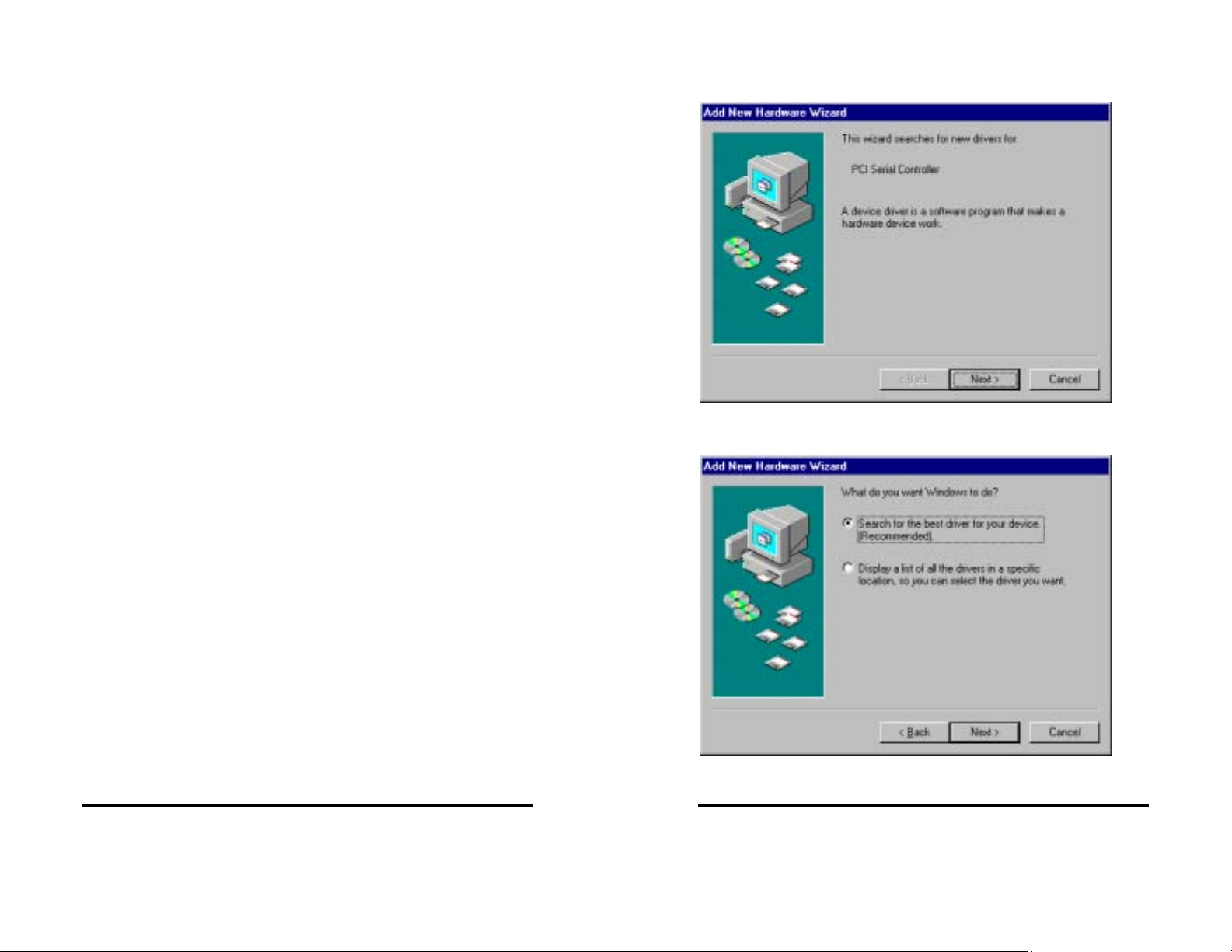
3. Windows will detect the PCI card, start the Add New Hardware
Wizard, and begin driver installation. When installation is
complete, Windows will set the hardware addressing & interrupt
using the drivers and the Plug and Play function of the
Operating System.
4. The driver installation proceeds in two parts: the first part
installs the driver for the PCI Serial card, the second part installs
the serial driver for each Com port on the card. After Port A
installation is finished, installation of Ports B, C, & D will proceed
without additional user input. (Port A=Port 1, Port D=Port 4)
continued next page
5. After new hardware is detected, this screen will appear. (W95:
This screen is named Update Device Driver Wizard.)
6. Click Next to continue. (W95: Insert the Driver Disk in Drive,
then click Next - skip to step 9.)
7. Click Next.
Documentation Number 3PCISD4x-3903 Manual Chapter 3 13
B&B Electronics Mfg Co – 707 Dayton Rd - PO Box 1040 - Ottawa IL 61350 - Ph 815-433-5100 - Fax 815-433-5104
B&B Electronics Ltd – Westlink Comm. Pk. – Oranmore, Galway, Ireland – Ph +353 91-792444 – Fax +353 91-792445
14 Chapter 3 Documentation Number 3PCISD4x-3903 Manual
B&B Electronics Mfg Co – 707 Dayton Rd - PO Box 1040 - Ottawa IL 61350 - Ph 815-433-5100 - Fax 815-433-5104
B&B Electronics Ltd – Westlink Comm. Pk. – Oranmore, Galway, Ireland – Ph +353 91-792444 – Fax +353 91-792445
Page 10

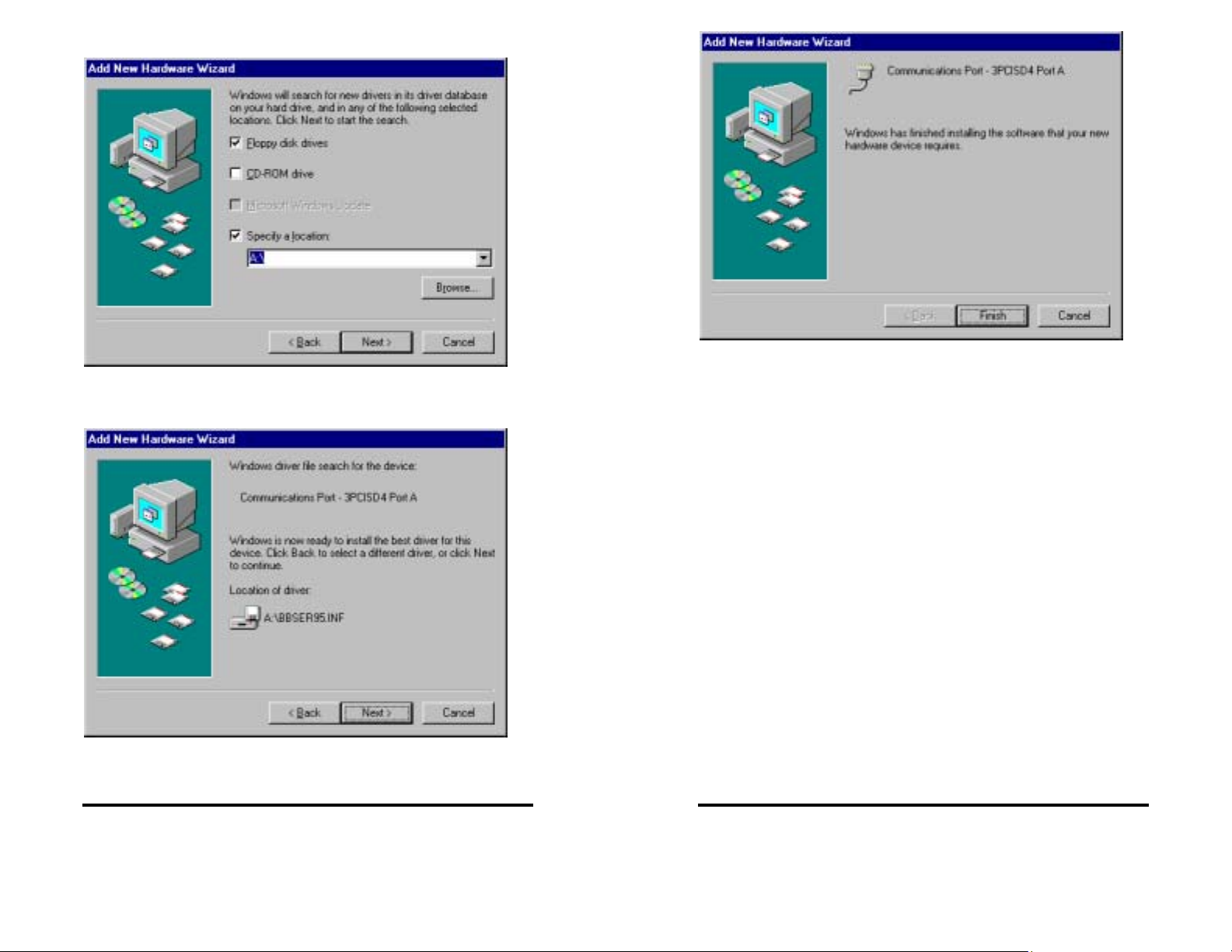
8. Select Floppy disk drives, Specify A:\
9. Insert the driver disk, then Click Next.
Windows will find “4-Port PCI Serial Adapter (3PCISD4)” and the
driver inf file. (W95: Driver name not shown - skip to step 11.)
10. Click Next.
11. Click Finish to begin the second part of the driver installation
which installs the Com port drivers for Port A , B, C & D.
12. Click Next. (W95: Skip to step 15.)
Documentation Number 3PCISD4x-3903 Manual Chapter 3 15
B&B Electronics Mfg Co – 707 Dayton Rd - PO Box 1040 - Ottawa IL 61350 - Ph 815-433-5100 - Fax 815-433-5104
B&B Electronics Ltd – Westlink Comm. Pk. – Oranmore, Galway, Ireland – Ph +353 91-792444 – Fax +353 91-792445
16 Chapter 3 Documentation Number 3PCISD4x-3903 Manual
B&B Electronics Mfg Co – 707 Dayton Rd - PO Box 1040 - Ottawa IL 61350 - Ph 815-433-5100 - Fax 815-433-5104
B&B Electronics Ltd – Westlink Comm. Pk. – Oranmore, Galway, Ireland – Ph +353 91-792444 – Fax +353 91-792445
Page 11
13. Click Next to continue. Re-insert the driver disk if needed.
Windows will find the Communications Port and inf file.
14. Click Next. (W95: Driver name not shown.)
15. Click Finish to complete Com driver installation.
The computer will finish Com driver installation for Port A, then
search, find and install the driver for Port B, then Port C, and Port D
without requiring any more user input.
16. Wait for the process to complete.
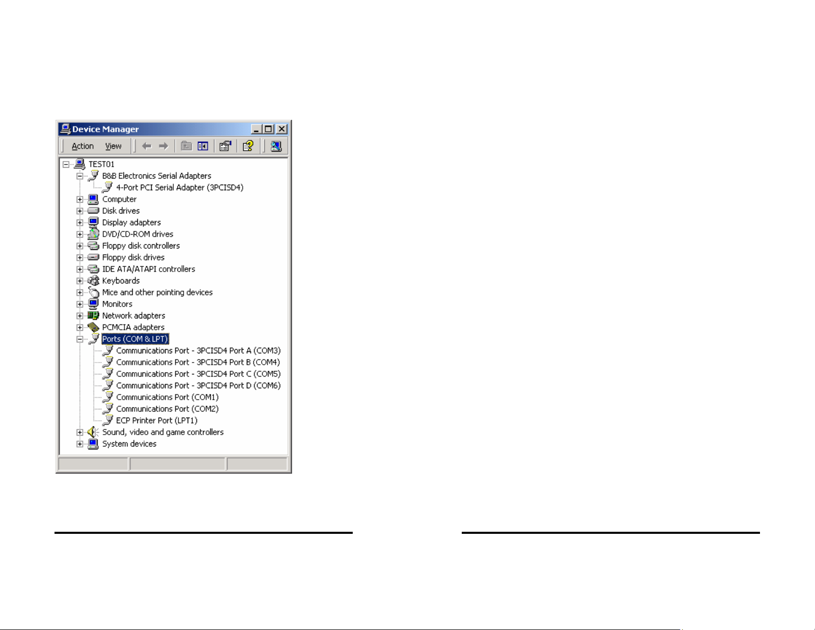
To verify the installation, open My Computer, Control Panel,
System (or Start, Setting, Control Panel, System).
Then select the Device Manager Tab.
continued next page
Documentation Number 3PCISD4x-3903 Manual Chapter 3 17
B&B Electronics Mfg Co – 707 Dayton Rd - PO Box 1040 - Ottawa IL 61350 - Ph 815-433-5100 - Fax 815-433-5104
B&B Electronics Ltd – Westlink Comm. Pk. – Oranmore, Galway, Ireland – Ph +353 91-792444 – Fax +353 91-792445
18 Chapter 3 Documentation Number 3PCISD4x-3903 Manual
B&B Electronics Mfg Co – 707 Dayton Rd - PO Box 1040 - Ottawa IL 61350 - Ph 815-433-5100 - Fax 815-433-5104
B&B Electronics Ltd – Westlink Comm. Pk. – Oranmore, Galway, Ireland – Ph +353 91-792444 – Fax +353 91-792445
Page 12

Removal of Card And Drivers
If you need to remove the card from your system or remove the
current driver before installing a possible future driver upgrade:
1. Open My Computer, Control Panel, System (or Start, Setting,
Control Panel, System).
2. Select the Device Manager Tab (see figure on previous page).
3. Click B&B Electronics Serial Adapters, then Select the 4-Port
PCI Serial Adapter (3PCISD4).
4. Click the Remove button.
5. Close the Windows, and Open My Computer, Drive C:
6. Open the Windows directory on your hard drive, then open the
Inf folder, then Other. (If the Inf folder is not shown, it is hidden.
Select View, Folder Options, Files and Folders, Show all files.
Win95: Select View, Options, View, Show all files.)
Click the B&B Electronics Serial Adapters device to view the
adapter. If you want other details, Select Properties.
Click Ports (COM & LPT) to view the COM numbers assigned by
Windows to the card.
The 3PCISD4x card will have 3PCISD4 Port A (COMx), Port B, Port
C and Port D. The COM port numbers will normally be COM5,
COM6 COM7 and COM8, if available.
17. You can now remove the driver disk, close the Window s, and
check the new ports with your software.
If your software requires accessing a COM port below COM5, and
you have unused COM numbers not occupied by a FAX/Modem or
other device, you can re-assign the PCI card COM numbers using
our B&B PnP COM Rename utility. Refer to Appendix E.
Documentation Number 3PCISD4x-3903 Manual Chapter 3 19
B&B Electronics Mfg Co – 707 Dayton Rd - PO Box 1040 - Ottawa IL 61350 - Ph 815-433-5100 - Fax 815-433-5104
B&B Electronics Ltd – Westlink Comm. Pk. – Oranmore, Galway, Ireland – Ph +353 91-792444 – Fax +353 91-792445
7. Remove the B&B INF files. (*BBMSER.INF &
*BBMSER95.INF) Close the Window.
8. Shut down the computer, then remove the card.
20 Chapter 3 Documentation Number 3PCISD4x-3903 Manual
B&B Electronics Mfg Co – 707 Dayton Rd - PO Box 1040 - Ottawa IL 61350 - Ph 815-433-5100 - Fax 815-433-5104
B&B Electronics Ltd – Westlink Comm. Pk. – Oranmore, Galway, Ireland – Ph +353 91-792444 – Fax +353 91-792445
Page 13

Windows 2000 Professional
This section covers device driver installation for Windows 2000
Professional.
Windows 2000 Server
Windows 2000 Advanced Server
Windows 2000 Data Center
1. Configure each port on the PCI card to the desired RS232/422/485 mode using the jumpers for Port 1, 2, 3, & 4.
2. Install the card in the slot, start the computer as an Administrator
or ask your system administrator to install the software.
3. Windows will detect the PCI card and start Found New
Hardware Wizard, to begin driver installation. When installation
is complete, Windows will set the ha rdware addressing &
interrupt using the drivers and the Plug and Play function of the
Operating System.
4. After the driver for the PCI Serial Card installs, the serial driver
for the Com port will be installed once for each port on the card.
6. Select Search, Click Next.
5. Click Next to continue.
Documentation Number 3PCISD4x-3903 Manual Chapter 3 21
B&B Electronics Mfg Co – 707 Dayton Rd - PO Box 1040 - Ottawa IL 61350 - Ph 815-433-5100 - Fax 815-433-5104
B&B Electronics Ltd – Westlink Comm. Pk. – Oranmore, Galway, Ireland – Ph +353 91-792444 – Fax +353 91-792445
7. Insert the driver disk in floppy disk drive A: Click Next.
22 Chapter 3 Documentation Number 3PCISD4x-3903 Manual
B&B Electronics Mfg Co – 707 Dayton Rd - PO Box 1040 - Ottawa IL 61350 - Ph 815-433-5100 - Fax 815-433-5104
B&B Electronics Ltd – Westlink Comm. Pk. – Oranmore, Galway, Ireland – Ph +353 91-792444 – Fax +353 91-792445
Page 14

8. Click Next.
The computer will finish the installation of the driver for the card,
then search for, find and install the Com driver for Port A, Port B,
Port C and Port D.
15. Wait for the process to complete.
Don't remove the floppy disk until you verify that Com ports have
been assigned to the card.
16. Open My Computer, Control Panel, System, then select the
Hardware Tab on System Properties.
17. Select the Device Manager button.
18. View the device list (next page).
9. Click Finish to complete the Instal l.
Documentation Number 3PCISD4x-3903 Manual Chapter 3 23
B&B Electronics Mfg Co – 707 Dayton Rd - PO Box 1040 - Ottawa IL 61350 - Ph 815-433-5100 - Fax 815-433-5104
B&B Electronics Ltd – Westlink Comm. Pk. – Oranmore, Galway, Ireland – Ph +353 91-792444 – Fax +353 91-792445
24 Chapter 3 Documentation Number 3PCISD4x-3903 Manual
B&B Electronics Mfg Co – 707 Dayton Rd - PO Box 1040 - Ottawa IL 61350 - Ph 815-433-5100 - Fax 815-433-5104
B&B Electronics Ltd – Westlink Comm. Pk. – Oranmore, Galway, Ireland – Ph +353 91-792444 – Fax +353 91-792445
Page 15
The 4-Port PCI Serial Adapter card is installed under B&B
Electronics Serial Adapters. This can be opened to show General,
Driver, Resources (Address settings & IRQ).
Under Ports, COM3 was assigned to Port A , and COM4 through
COM6 was assigned to Port B, C and D. (Port 1=A, 2=B, 3=C &
4=D)
Removal of Card & Drivers
If you need to remove the card from your system or remove the
current driver before installing a possible future driver upgrade:
Refer to the figure on the prior page:
1. Click on 3PCISD4 Port D under Ports (COM & LPT), and select
Uninstall (right click). Repeat for Port C, B, and A.
2. Next Click on 4-Port PCI Serial Adapter (3PCISD4) under B&B
Electronics. Select Uninstall.
3. Remove the two sets of driver files from the Windows INF
directory. (These are named by the OS in the sequence of
installation. On a clean system they are: Oem0.inf & Oem0.PNF
and Oem1.inf & Oem1.PNF. The .inf versions should be verified
by opening it with Notepad, then checking that it is a B&B
Electronics file. The PNF version is a compiled copy of the
same information.)
You can use the Find, File or Folder function to search for the
text B&B within the files.
You may need to set your Views (under My Computer to show
all files and folders if the INF directory and .inf files are not
visible.
4. Shut down the system and remove the card.
19. You can now remove the driver disk, close the Windows and
check the new Com ports with your software.
Documentation Number 3PCISD4x-3903 Manual Chapter 3 25
B&B Electronics Mfg Co – 707 Dayton Rd - PO Box 1040 - Ottawa IL 61350 - Ph 815-433-5100 - Fax 815-433-5104
B&B Electronics Ltd – Westlink Comm. Pk. – Oranmore, Galway, Ireland – Ph +353 91-792444 – Fax +353 91-792445
26 Chapter 3 Documentation Number 3PCISD4x-3903 Manual
B&B Electronics Mfg Co – 707 Dayton Rd - PO Box 1040 - Ottawa IL 61350 - Ph 815-433-5100 - Fax 815-433-5104
B&B Electronics Ltd – Westlink Comm. Pk. – Oranmore, Galway, Ireland – Ph +353 91-792444 – Fax +353 91-792445
Page 16

WINDOWS NT 4.0
1. Configure each port on the PCI card to the desired RS232/422/485 mode using the jumpers for Port 1, 2, 3, & 4.
2. Install the card in the slot, start the computer, and log on to
Windows NT 4.0 as an Administrator or ask your system
administrator to install the software.
3. Open the Control Panel. (Select Start, Settings.)
4. Select Add/Remove Programs.
5. Click the Install button, then click Next.
6. Insert the driver disk into drive A:
7. Enter A:\WinNT40\Setup.exe in the Command line for
installation program window (as above).
8. Click Finish to start the Setup program.
Documentation Number 3PCISD4x-3903 Manual Chapter 3 27
B&B Electronics Mfg Co – 707 Dayton Rd - PO Box 1040 - Ottawa IL 61350 - Ph 815-433-5100 - Fax 815-433-5104
B&B Electronics Ltd – Westlink Comm. Pk. – Oranmore, Galway, Ireland – Ph +353 91-792444 – Fax +353 91-792445
9. Click Next. Follow the instructions until completed.
28 Chapter 3 Documentation Number 3PCISD4x-3903 Manual
B&B Electronics Mfg Co – 707 Dayton Rd - PO Box 1040 - Ottawa IL 61350 - Ph 815-433-5100 - Fax 815-433-5104
B&B Electronics Ltd – Westlink Comm. Pk. – Oranmore, Galway, Ireland – Ph +353 91-792444 – Fax +353 91-792445
Page 17

10. This driver does not require re-booting to complete installation.
11. Open the Control Panel, select Ports.
12. Verify 4 new COM Ports (COM5, COM6, COM7, COM8).
If you have 4 new COM ports, the installation is complete. Select
one of the new ports, select Settings, Advanced. You should obtain
the message, "There are no user configurable advanced I/O
parameters for this COM port."
Check the ports with your software or with a Loopback test (see
page 33).
Note: In the above example, a serial mouse is connected to the port
which would usually be COM1. NT does not show it. COM2 is the
second built-in serial port.
You can check details of the serial card setup using Windows NT
Diagnostics, found under Administrative Tools. This can show the
Resources used such as addresses and IRQ.
Windows Diagnostics will not allow changing anything.
The above shows the 4 ports using the PCI card interrupt.
Documentation Number 3PCISD4x-3903 Manual Chapter 3 29
B&B Electronics Mfg Co – 707 Dayton Rd - PO Box 1040 - Ottawa IL 61350 - Ph 815-433-5100 - Fax 815-433-5104
B&B Electronics Ltd – Westlink Comm. Pk. – Oranmore, Galway, Ireland – Ph +353 91-792444 – Fax +353 91-792445
30 Chapter 3 Documentation Number 3PCISD4x-3903 Manual
B&B Electronics Mfg Co – 707 Dayton Rd - PO Box 1040 - Ottawa IL 61350 - Ph 815-433-5100 - Fax 815-433-5104
B&B Electronics Ltd – Westlink Comm. Pk. – Oranmore, Galway, Ireland – Ph +353 91-792444 – Fax +353 91-792445
Page 18
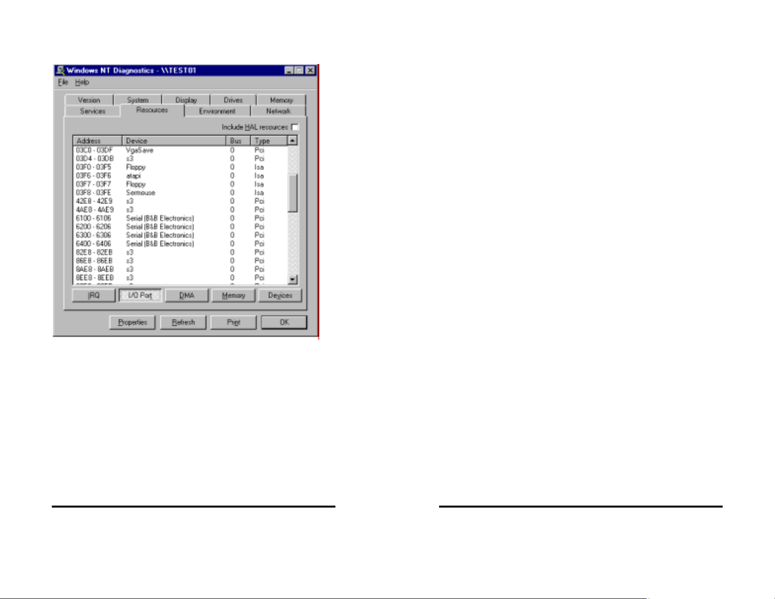
The screen below shows the address range for each serial port on
the B&B Electronics 4 port Serial Card.
Removal of Card and Driver
If you need to remove the card from your system or remove the
current driver before installing a possible future driver upgrade:
1. Open the Windows NT subdirectory.
2. Open System32.
3. Open Drivers.
4. Find the "Bbserial.Sys" file and delete it.
5. Shut down the system.
6. Remove the 4-Port PCI Serial Adapter card.
Documentation Number 3PCISD4x-3903 Manual Chapter 3 31
B&B Electronics Mfg Co – 707 Dayton Rd - PO Box 1040 - Ottawa IL 61350 - Ph 815-433-5100 - Fax 815-433-5104
B&B Electronics Ltd – Westlink Comm. Pk. – Oranmore, Galway, Ireland – Ph +353 91-792444 – Fax +353 91-792445
32 Chapter 3 Documentation Number 3PCISD4x-3903 Manual
B&B Electronics Mfg Co – 707 Dayton Rd - PO Box 1040 - Ottawa IL 61350 - Ph 815-433-5100 - Fax 815-433-5104
B&B Electronics Ltd – Westlink Comm. Pk. – Oranmore, Galway, Ireland – Ph +353 91-792444 – Fax +353 91-792445
Page 19

Chapter 4: TROUBLESHOOTING
If you have any trouble starting your system after installing the card,
the card may not be properly seated in the slot. Remove and reinsert it or try a different slot.
If you are unable to communicate with the card using your software
and hardware devices:
1. Check your pinouts. In RS-422 or RS-485 mode the "A" lines
should match your "A" or "−" lines. "B" lines should match your
"B" or "+" lines. Note: RS-422/485 pinouts are non-standard.
2. Use the COMTest program provided on the PCI/USB Port Utility
Disk with a loop back to check the card. Run Setup.exe to install
COMTest on your program menu under B&B Electronics.
A Loopback connection for RS-232 connects the Transmit
output to the Receive input. (pins #2 & #3 on the DB9
connector) For RS-422 or 4-wire RS-485, connect the TD(A) to
RD(A) and the TD(B) to RD(B). Then use the COMTest program
to send characters, and observe the characters being received.
To check 2-wire RS-485, you will need to enable the receiver by
moving the receive jumper to 422 mode, or use one Port to
transmit to another by cross connecting and loading COMTest
twice, one copy for each port. Characters typed in one copy of
COMTest will appear in the receive window of the other. Note
that software must ignore the RS-232 handshaking lines in RS422/RS-485 mode, the input lines (CTS, DSR, DCD, RI) are not
pulled high.
3. Try another software package for troubleshooting.
4. Check our website for available FAQ's or troubleshooting hints.
5. Call B&B Electronics Technical Support for troubleshooting
assistance.
International Office
Technicians are available at (815) 433-5100 to answer your
questions from 8 AM - 5 PM weekdays (Central Time).
European Office
Technicians are available at +353 91-792444 to answer your
questions from 8:30 AM – 5 PM weekdays (GMT Time).
Documentation Number 3PCISD4x-3903 Manual Chapter 4 33
B&B Electronics Mfg Co – 707 Dayton Rd - PO Box 1040 - Ottawa IL 61350 - Ph 815-433-5100 - Fax 815-433-5104
B&B Electronics Ltd – Westlink Comm. Pk. – Oranmore, Galway, Ireland – Ph +353 91-792444 – Fax +353 91-792445
34 Chapter 4 Documentation Number 3PCISD4x-3903 Manual
B&B Electronics Mfg Co – 707 Dayton Rd - PO Box 1040 - Ottawa IL 61350 - Ph 815-433-5100 - Fax 815-433-5104
B&B Electronics Ltd – Westlink Comm. Pk. – Oranmore, Galway, Ireland – Ph +353 91-792444 – Fax +353 91-792445
Page 20

Appendix A: DB9 Signal Connections
Table 7: RS-232 Pinouts
RS-232
Signal
Description Direction DB9M
Pin
DCD Data Carrier Detect input 1
RD Receive Data input 2
TD Transmit Data output 3
DTR Data Terminal Ready output 4
GND Signal Ground ---- 5
DSR Data Set Ready input 6
RTS Request to Send output 7
CTS Clear to Send input 8
RI Ring Indicator Input 9
Table 8: RS-422/RS-485 Pinouts
RS-422
signal
-- -- 1
RD(A) −
TD(A) −
-- -- 4
GND Signal Ground ---- 5
-- -- 6
TD(B) + Transmit Data B output 7
RD(B) + Receive Data B input 8
-- NA 9
With 2-wire RS-485 mode operation, your connection cable must
jumper RD(A) to TD(A) and RD(B) to TD(B). Connect from TD(A) &
TD(B) to the Data A(−) and Data B(+) wires of your RS-485 network.
The EIA RS-422 Specification labels data lines with an "A" and "B"
designator. Some RS-422 equipment uses a "−" and "+" designator.
In almost all cases, the "A" line is the equivalent of the "−" line and
the "B" line is the equivalent of the "+" line. See our RS-422/485
Application Note (available on our websites).
Description Direction DB9M
Pinout
Receive Data A input 2
Transmit Data A output 3
Documentation Number 3PCISD4x-3903 Manual Appendix A A-1
B&B Electronics Mfg Co – 707 Dayton Rd - PO Box 1040 - Ottawa IL 61350 - Ph 815-433-5100 - Fax 815-433-5104
B&B Electronics Ltd – Westlink Comm. Pk. – Oranmore, Galway, Ireland – Ph +353 91-792444 – Fax +353 91-792445
A-2 Appendix A Documentation Number 3PCISD4x-3903 Manual
B&B Electronics Mfg Co – 707 Dayton Rd - PO Box 1040 - Ottawa IL 61350 - Ph 815-433-5100 - Fax 815-433-5104
B&B Electronics Ltd – Westlink Comm. Pk. – Oranmore, Galway, Ireland – Ph +353 91-792444 – Fax +353 91-792445
Page 21

Appendix B: Jumper Mode Tables
Port A Jumper Settings Mode Table
Jumpers
Port A (1)
JP1
(4 Jumpers)
JP3A MODE 232 422/485 422/485 422/485
JP3B RX not used 422 422 485
JP3C TX not used 422 485 485
JP3D (SD/RTS)
(typical)
JP3E - Term
120Ω (typical)
JP5 Clock
(x4 or x1)
(typical)
How to use the table: The left vertical column shows the jumpers
for port A. The right 4 vertical columns show the position setting of
the jumper at the left for RS-232, RS-422 or 4-wire RS-485 or 2-wire
RS-485 modes.
NOTES:
Refer to the Setup section for explanations of the RTS/SD,
Termination and Clock settings. All ports share the Clock setting.
RS-485 Mode: The SD/RTS jumpers should be set to automatic SD
unless your software requires RTS Control.
Note that termination should only be used in systems with both high
baud rates (>19200) and over several thousand feet of cable.
Information on RS-422 and RS-485 communications can be found in
the B&B Electronics RS-422/485 Application Note (available on our
Website).
RS-232 RS-422
232 422 422 422
not used not used RTS/SD
not used IN/OUT
*4/*1
*1
4-wire
OUT
*4/*1
*1
RS-485
4-wire
SD
IN/OUT
OUT
*4/*1
*1
RS-485
2-wire
RTS/SD
SD
IN/OUT
OUT
*4/*1
*1
Port B Jumper Settings Mode Table
Jumpers
Port B (2)
JP2
(4 Jumpers)
JP4A MODE 232 422/485 422/485 422/485
JP4B RX not used 422 422 485
JP4C TX not used 422 485 485
JP4D (SD/RTS)
(typical)
JP4E - Term
120Ω
(typical)
JP5 Clock
(x4 or x1)
(typical)
RS-232 RS-422
232 422 422 422
not used not used RTS/SD
not used IN/OUT
*4/*1
*1
4-wire
OUT
*4/*1
*1
RS-485
4-wire
SD
IN/OUT
OUT
*4/*1
*1
RS-485
2-wire
RTS/SD
SD
IN/OUT
OUT
*4/*1
*1
How to use the table: The left vertical column shows the jumpers
for Port B. The right 4 vertical columns show the setting of the
jumper at the left for RS-232, RS-422 or 4-wire RS-485 or 2-wire
RS-485 modes.
NOTES:
Refer to the Setup section for explanations of the RTS/SD,
Termination and Clock settings. All ports share the Clock setting.
RS-485 Mode: The SD/RTS jumpers should be set to automatic SD
unless your software requires RTS Control.
Note that termination should only be used in systems with both high
baud rates (>19200) and over several thousand feet of cable.
Information on RS-422 and RS-485 communications can be found in
the B&B Electronics RS-422/485 Application Note (available on our
Website).
Documentation Number 3PCISD4x-3903 Manual Appendix B B-1
B&B Electronics Mfg Co – 707 Dayton Rd - PO Box 1040 - Ottawa IL 61350 - Ph 815-433-5100 - Fax 815-433-5104
B&B Electronics Ltd – Westlink Comm. Pk. – Oranmore, Galway, Ireland – Ph +353 91-792444 – Fax +353 91-792445
B-2 Appendix B Documentation Number 3PCISD4x-3903 Manual
B&B Electronics Mfg Co – 707 Dayton Rd - PO Box 1040 - Ottawa IL 61350 - Ph 815-433-5100 - Fax 815-433-5104
B&B Electronics Ltd – Westlink Comm. Pk. – Oranmore, Galway, Ireland – Ph 353-91-792444 – Fax 353-91-792445
Page 22

Port C Jumper Settings Mode Table
Jumpers
Port C (3)
JP8
(4 Jumpers)
JP6A MODE 232 422/485 422/485 422/485
JP6B RX not used 422 422 485
JP6C TX not used 422 485 485
JP6D (SD/RTS)
(typical)
JP6E - Term
120Ω
(typical)
JP5 Clock
(x4 or x1)
(typical)
RS-232 RS-422
232 422 422 422
not used not used RTS/SD
not used IN/OUT
*4/*1
*1
4-wire
OUT
*4/*1
*1
RS-485
4-wire
SD
IN/OUT
OUT
*4/*1
*1
RS-485
2-wire
RTS/SD
SD
IN/OUT
OUT
*4/*1
*1
How to use the table: The left vertical column shows the jumpers
for port C. The right 4 vertical columns show the position setting of
the jumper at the left for RS-232, RS-422, 4-wire RS-485 or 2-wire
RS-485 modes.
NOTES:
Refer to the Setup section for explanations of the RTS/SD,
Termination and Clock settings. All ports share the Clock setting.
RS-485 Mode: The SD/RTS jumpers should be set to automatic SD
unless your software requires RTS Control.
Note that termination should only be used in systems with both high
baud rates (>19200) and over several thousand feet of cable.
Information on RS-422 and RS-485 communications can be found in
the B&B Electronics RS-422/485 Application Note (available on our
Website).
Port D Jumper Settings Mode Table
Jumpers
Port D (4)
JP9
(4 Jumpers)
JP7A MODE 232 422/485 422/485 422/485
JP7B RX not used 422 422 485
JP7C TX not used 422 485 485
JP7D (SD/RTS)
(typical)
JP7E - Term
120Ω (typical)
JP5 Clock
(x4 or x1)
(typical)
RS-232 RS-422
232 422 422 422
not used not used RTS/SD
not used IN/OUT
*4/*1
*1
4-wire
OUT
*4/*1
*1
RS-485
4-wire
SD
IN/OUT
OUT
*4/*1
*1
RS-485
2-wire
RTS/SD
SD
IN/OUT
OUT
*4/*1
*1
How to use the table: The left vertical column shows the jumpers
for port D. The right 4 vertical columns show the position setting of
the jumper at the left for RS-232, RS-422, 4-wire RS-485 or 2-wire
RS-485 modes.
NOTES:
Refer to the Setup section for explanations of the RTS/SD,
Termination and Clock settings. All ports share the Clock setting.
RS-485 Mode: The SD/RTS jumpers should be set to automatic SD
unless your software requires RTS Control.
Note that termination should only be used in systems with both high
baud rates (>19200) and over several thousand feet of cable.
Information on RS-422 and RS-485 communications can be found in
the B&B Electronics RS-422/485 Application Note (available on our
Website).
Documentation Number 3PCISD4x-3903 Manual Appendix B B-3
B&B Electronics Mfg Co – 707 Dayton Rd - PO Box 1040 - Ottawa IL 61350 - Ph 815-433-5100 - Fax 815-433-5104
B&B Electronics Ltd – Westlink Comm. Pk. – Oranmore, Galway, Ireland – Ph +353 91-792444 – Fax +353 91-792445
B-4 Appendix B Documentation Number 3PCISD4x-3903 Manual
B&B Electronics Mfg Co – 707 Dayton Rd - PO Box 1040 - Ottawa IL 61350 - Ph 815-433-5100 - Fax 815-433-5104
B&B Electronics Ltd – Westlink Comm. Pk. – Oranmore, Galway, Ireland – Ph 353-91-792444 – Fax 353-91-792445
Page 23

Appendix C: 3PCISD4 I/O Pinout
Signal DB-37 Pinout
CD Port 1 Pin 1
RX/RDA Port 1 Pin 2
TX/RDA Port 1 P i n 3
DTR Port 1 Pin 4
GND Pin 5
DSR Port 1 Pin 20
RTS/TDB Port 1 Pin 21
CTS/RDB Port 1 Pin 22
RI Port 1 Pin 23
CD Port 2 Pin 6
RX/RDA Port 2 Pin 7
TX/RDA Port 2 P i n 8
DTR Port 2 Pin 9
GND Pin 24
DSR Port 2 Pin 25
RTS/TDB Port 2 Pin 26
CTS/RDB Port 2 Pin 27
RI Port 2 Pin 28
CD Port 3 Pin 10
RX/RDA Port 3 Pin 11
TX/RDA Port 3 P i n 12
DTR Port 3 Pin 13
GND Pin 14
DSR Port 3 Pin 29
RTS/TDB Port 3 Pin 30
CTS/RDB Port 3 Pin 31
RI Port 3 Pin 32
CD Port 4 Pin 15
RX/RDA Port 4 Pin 16
TX/RDA Port 4 P i n 17
DTR Port 4 Pin 18
GND Pin 33
DSR Port 4 Pin 34
RTS/TDB Port 4 Pin 35
CTS/RDB Port 4 Pin 36
RI Port 4 Pin 37
NA Pin 19
Documentation Number 3PCISD4x-3903 Manual Appendix C C-1
B&B Electronics Mfg Co – 707 Dayton Rd - PO Box 1040 - Ottawa IL 61350 - Ph 815-433-5100 - Fax 815-433-5104
B&B Electronics Ltd – Westlink Comm. Pk. – Oranmore, Galway, Ireland – Ph +353 91-792444 – Fax +353 91-792445
C-2 Appendix C Documentation Number 3PCISD4x-3903 Manual
B&B Electronics Mfg Co – 707 Dayton Rd - PO Box 1040 - Ottawa IL 61350 - Ph 815-433-5100 - Fax 815-433-5104
B&B Electronics Ltd – Westlink Comm. Pk. – Oranmore, Galway, Ireland – Ph +353 91-792444 – Fax +353 91-792445
Page 24

Appendix D: 3PCISD4 I/O Schemat ic
Port 1 I/O Schematic
Documentation Number 3PCISD4x-3903 Manual Appendix D D-1
B&B Electronics Mfg Co – 707 Dayton Rd - PO Box 1040 - Ottawa IL 61350 - Ph 815-433-5100 - Fax 815-433-5104
B&B Electronics Ltd – Westlink Comm. Pk. – Oranmore, Galway, Ireland – Ph +353 91-792444 – Fax +353 91-792445
D-2 Appendix D Documentation Number 3PCISD4x-3903 Manual
B&B Electronics Mfg Co – 707 Dayton Rd - PO Box 1040 - Ottawa IL 61350 - Ph 815-433-5100 - Fax 815-433-5104
B&B Electronics Ltd – Westlink Comm. Pk. – Oranmore, Galway, Ireland – Ph +353 91-792444 – Fax +353 91-792445
Page 25

Appendix E: Renaming COM Ports - Win 95/98/ ME
Renaming PCI COM Ports Using the PnP COM Rename Utility
CAUTION: You must be using Windows 95/98 or ME. This utility is
not designed for NT or other Windows versions.
This program edits the registry directly, it will only change entries
related to B&B PCI or USB Serial Ports. Improper use of this
program can cause conflicts with other COM Ports installed on your
computer.
Renaming COM ports will only affect software that accesses COM
ports through Windows, not software that accesses ports from DOS
or at the hardware level.
This program should only be used after all serial ports have been
installed.
Windows 95/98 and ME automatically assigns COM port numbers
starting at COM5 when the port is not at the standard base
addresses for COM1 to COM4.
If your software refuses to access COM ports above COM4, and you
have unused COM numbers that you want to be able use with your
B&B PCI Serial Card, this utility can be used to rename some or all
of the ports to the unused COM numbers.
First, check the ports list shown in the Device Manager, then check
any Modem or FAX device to make sure that the port number isn't
being used for a FAX/Modem or Network Redirector.
If you have built-in ports you want to disable from the BIOS in order
to use your PCI card at that COM number, first remove the port with
the Device Manager. Then re-boot to the BIOS, disable the port with
hardware settings, Exit with a "Save Settings", then re-start
Windows Next, verify the port number is not present. Then use the
Rename utility to rename the PCI card ports as needed.
To Remove a Port: Choose Settings, Control Panel, System, Device
Manager, then select the port to highlight it. Click Remove below the
window. To remove all B&B PCI ports, select the B&B Serial
Adapter. This clears registry entries for the card and ports.
Install the PCI/USB COM Port Utilities
(1) To use the PnP COM Rename utility, insert the PCI/USB COM
Port Utility Disk and run Setup.exe. This will install COMTest
and PnP COM Rename under Programs, B&B Electronics.
(2) The Rename utility will not be installed if you are running
Windows 2000 or NT.
Using PnP COM Rename
(1) Shut down all programs that are accessing any Com ports.
(2) Start the PnP COM Rename Utility from the Programs menu
under B&B Electronics.
(3) Read the Cautionary Warnings, it is possible to rename a PCI or
USB serial port to a number already in use which will cause
problems. If any problems occur after renaming, you may need
to re-start the system and rerun the Rename utility to correct the
situation or remove the serial card in the Device Manager. Then
Refresh the Device Manager to detect the card and re-install the
drivers. Determine which renamed COM port caused the
problem, and do not use that name for a renamed port.
(4) Accept the conditions of use by clicking Yes or click No to exit.
(5) Select the currently named COM port number you want to
change in the left window, then the new number in the right
window. Then click Finish. Repeat for other ports as needed.
Documentation Number 3PCISD4x-3903 Manual Appendix E E-1
B&B Electronics Mfg Co – 707 Dayton Rd - PO Box 1040 - Ottawa IL 61350 - Ph 815-433-5100 - Fax 815-433-5104
B&B Electronics Ltd – Westlink Comm. Pk. – Oranmore, Galway, Ireland – Ph +353 91-792444 – Fax +353 91-792445
E-2 Appendix E Documentation Number 3PCISD4x-3903 Manual
B&B Electronics Mfg Co – 707 Dayton Rd - PO Box 1040 - Ottawa IL 61350 - Ph 815-433-5100 - Fax 815-433-5104
B&B Electronics Ltd – Westlink Comm. Pk. – Oranmore, Galway, Ireland – Ph +353 91-792444 – Fax +353 91-792445
Page 26

(6) If the PCI card was previously installed and not removed in the
Device Manager, you may find several B&B COM ports with the
same number. The last instance of the same number is usually
the most recent installation. Only the active ports can be
renamed with the program to show the new name under the
Device Manager. Inactive port numbers will not show any
change after renaming. Ideally, unused entries should be
removed by using RegEdit, then having the system re-install the
drivers to make the entries. This will result in a single entry for
each port on the card, and only that entry will need to be
changed.
(7) After all B&B PCI or USB COM ports have been renumbered as
needed, click Close to exit.
If you need to install another serial device after using renaming with
this utility, you must:
(1) Name all COM Ports back to original settings using this
program.
(2) Install the new device according to manufacturer directions.
(3) Use this utility to rename the B&B COM Ports again as needed.
Documentation Number 3PCISD4x-3903 Manual Appendix E E-3
B&B Electronics Mfg Co – 707 Dayton Rd - PO Box 1040 - Ottawa IL 61350 - Ph 815-433-5100 - Fax 815-433-5104
B&B Electronics Ltd – Westlink Comm. Pk. – Oranmore, Galway, Ireland – Ph +353 91-792444 – Fax +353 91-792445
E-4 Appendix E Documentation Number 3PCISD4x-3903 Manual
B&B Electronics Mfg Co – 707 Dayton Rd - PO Box 1040 - Ottawa IL 61350 - Ph 815-433-5100 - Fax 815-433-5104
B&B Electronics Ltd – Westlink Comm. Pk. – Oranmore, Galway, Ireland – Ph +353 91-792444 – Fax +353 91-792445
Page 27

Appendix F: Declaration of Conformity
Manufacturer’s Name: B&B Electronics Manufacturing Company
DECLARATION OF CONFORMITY
Manufacturer’s Address: P.O. Box 1040
707 Dayton Road
Model Numbers: 3PCISD4 a/b
Description: Four Port PCI Serial Card
Type: Light industrial ITE equipment
Application of Council Directive: 89/336/EEC
Standards: EN 55022
EN 61000-6-1
EN 61000 (-4-2, -4-3, -4-4, -4-5, -4-6, -4-8, -4-11)
William H. Franklin III, Director of Engineering
Ottawa, IL 61350 USA
Documentation Number 3PCISD4x-3903 Manual Appendix F F-1
B&B Electronics Mfg Co – 707 Dayton Rd - PO Box 1040 - Ottawa IL 61350 - Ph 815-433-5100 - Fax 815-433-5104
B&B Electronics Ltd – Westlink Comm. Pk. – Oranmore, Galway, Ireland – Ph +353 91-792444 – Fax +353 91-792445
F-2 Appendix F Documentation Number 3PCISD4x-3903 Manual
B&B Electronics Mfg Co – 707 Dayton Rd - PO Box 1040 - Ottawa IL 61350 - Ph 815-433-5100 - Fax 815-433-5104
B&B Electronics Ltd – Westlink Comm. Pk. – Oranmore, Galway, Ireland – Ph +353 91-792444 – Fax +353 91-792445
 Loading...