

Page 1

Quadrature Encoder Counter Board
Models: 2IQEC2 2IQEC4
Documentation Number 2IQEC2/43798
This product
Designed and Manufactured
In Ottawa, Illinois
USA
of domestic and imported parts by
B&B Electronics Mfg. Co. Inc.
707 Dayton Rd. P.O. Box 1040 -- Ottawa, IL 61350
PH (815) 433-5100 -- FAX (815) 433-5105
Internet:
http://www.bb-elec.com
orders@bb-elec.com
support@bb.elec.com
1998 B&B Electronics -- September 1998
2IQEC2/43798 Manual Cover Page
B&B Electronics -- PO Box 1040 -- Ottawa, IL 61350
PH (815) 433-5100 -- FAX (815) 433-5105
Page 2

Table of Contents
CHAPTER 1: INTRODUCTION............................................................ 1
P
ACKING LIST...........................................................................................1
A
DDRESS SWITCH SETUP..........................................................................1
S
PECIFICATIONS........................................................................................ 2
CHAPTER 2: INSTALLATION............................................................. 3
OFTWARE INSTALLATION........................................................................ 3
S
I
NSTALLING THE CARD ............................................................................. 3
C
ARD SETTINGS........................................................................................ 3
Address................................................................................................. 3
IRQ....................................................................................................... 5
Configuring the jumpers ...................................................................... 6
S
OFTWARE REGISTERS.............................................................................. 8
Flag Register........................................................................................ 8
Reset and Load Signal Decoders (RLD).............................................. 8
Counter Mode Registers (CMR) .......................................................... 9
Input/Output Control Register (IOR)................................................. 10
Index Control Registers (IDR)........................................................... 11
CHAPTER 3: TROUBLESHOOTING..................................................12
APPENDIX A: HARDWARE I/O MAP.............................................A-1
I/O M
AP OF XT CLASS MACHINES.......................................................A-1
H
ARDWARE I/O MAP OF AT CLASS MACHINES................................... A-2
APPENDIX B: SPECIFICATIONS/TIMING DIAGRAMS............. B-1
IN DESCRIPTION.................................................................................B-1
P
A
DDRESSES........................................................................................... B-1
T
RANSIENT CHARACTERISTICS............................................................. B-2
Quadrature Mode............................................................................. B-2
Non-Quadrature Mode..................................................................... B-2
APPENDIX C: TYPICAL SET-UP EXAMPLES..............................C-1
2IQEC2/43798 Manual Table of Contents i
B&B Electronics -- PO Box 1040 -- Ottawa, IL 61350
PH (815) 433-5100 -- FAX (815) 433-5105
Page 3

Chapter 1: Introduction
The 2IQEC2/4 is a 2/4 channel quadrature encoder 24 bit
counter card used to track the position of up to 4 separate
encoders. This card is an ISA card that can be used in either an 8
or 16 bit slot. This card allows the computer to keep track of
position without a lot of CPU overhead, freeing it up for more
important tasks.
The 2IQEC2/4 offers a huge amount of flexibility. Upon a
borrow or carry the card can be configured to reset, load a preset,
cause an interrupt request or simply send out a TTL signal to
indicate the carry or borrow. The card contains two inputs that can
be configured to clear the counter or load the preset into the
counter. The index lines may also be used to clear the counter,
load the preset or cause an interrupt. The four channels use IRQ
sharing to prevent all the computer's resources from being taken up
by this card. The interrupt service routine can poll the card to find
out which channel caused the interrupt request.
Packing List
Examine the shipping carton and contents for physical damage.
The following items should be in the shipping carton:
1. 2IQEC2 or 2IQEC4
2. 2IQEC2/4 3.5" disk
3. This instruction manual
If any of these items are damaged or missing contact B&B
Electronics immediately.
Address Switch Setup
The 2IQEC2/4 cards use a 7-position DIP switch to program
the binary I/O address of each port on the card. The 2IQEC2/4
cards are factory configured for address 0x300 with no IRQ. If you
plan on installing the 2IQEC2/4 with these settings, check the switch
settings to ensure that they did not get inadvertently changed during
shipping.
2IQEC2/43798 Manual 1
B&B Electronics -- PO Box 1040 -- Ottawa, IL 61350
PH (815) 433-5100 -- FAX (815) 433-5105
Page 4

Specifications
Bus: IBM PC ISA Bus
Slot: Requires 1 full length slot for complete IRQ selectability.
When installed in a short slot, IRQs 10-15 will not be available.
The four channel card requires an additional space to mount the
connectors in the back panel. This space does not need a slot
on the motherboard.
Dimensions: 8.75" x 4.4"
I/O connection: 15-pin female D-sub connectors
Interrupt: IRQ 2-7, 10-12, 14, or 15.
Address: Switch programmable, 0 to hex 7F0
RS-422 Differential inputs
Differential input high-threshold voltage 0.2V maximum
Differential input low threshold voltage -0.2V maximum
Input differential voltage range 1.5 to 6 volts
TTL inputs
Input high threshold 2 V Maximum
Input low threshold 0.7 V Maximum
Input voltage range -0.2 to 5.5 volts
TTL outputs
1 mA source @ 4.375 V
5mAsink@0.5V
12 MHz count rate in quadrature 4X mode.
24-bit counters for up to four axes on 2IQEC4
(two axes on 2IQEC2)
Digital filtering of the quadrature clocks
Power Consumption
+5 VDC @ 250 mA
(See additional specifications in Appendix B.)
2 2IQEC2/43798 Manual
B&B Electronics -- PO Box 1040 -- Ottawa, IL 61350
PH (815) 433-5100 -- FAX (815) 433-5105
Page 5

Chapter 2: Installation
Software Installation
The 2IQEC2/4 comes with a useful example program. This
example program may be used royalty free when used with the B&B
Electronics 2IQEC2/4. Any other use is strictly prohibited. To install
this example file on your hard drive:
1. Place the disk in drive A:
2. Type A: and press the <ENTER> key.
3. Type Install and press the <ENTER> key.
4. Follow the instructions given by the program.
Installing the Card
1. Turn the power to your computer off.
2. Remove the cover of the computer. Be sure to use proper
grounding techniques.
3. Pick any full length (16-bit) unused slot. Although the 2IQEC2/4
cards will work in a short (8-bit) slot, IRQ's 10-15 will not be
available.
4. Remove the expansion slot cover. Save the screw for
installation of the 2IQEC2/4 card.
5. Set the address, IRQ, and other jumper settings. See Card
Settings in the next section for instructions on setting the
address and IRQ.
6. Install the 2IQEC2/4 card into the unused slot. Be certain that
the card is inserted completely into the slot.
7. Secure the card with the mounting screw.
Card Settings
Address
Switch S1 configures the address of the card. Switches
represent a 0 in the ON position, 1 when OFF. The address lines
are labeled on the card. SA10 is the MSB and SA4 is the LSB.
Table 1 shows the numerical weight and electrical connection of
each switch position.
2IQEC2/43798 Manual 3
B&B Electronics -- PO Box 1040 -- Ottawa, IL 61350
PH (815) 433-5100 -- FAX (815) 433-5105
Page 6
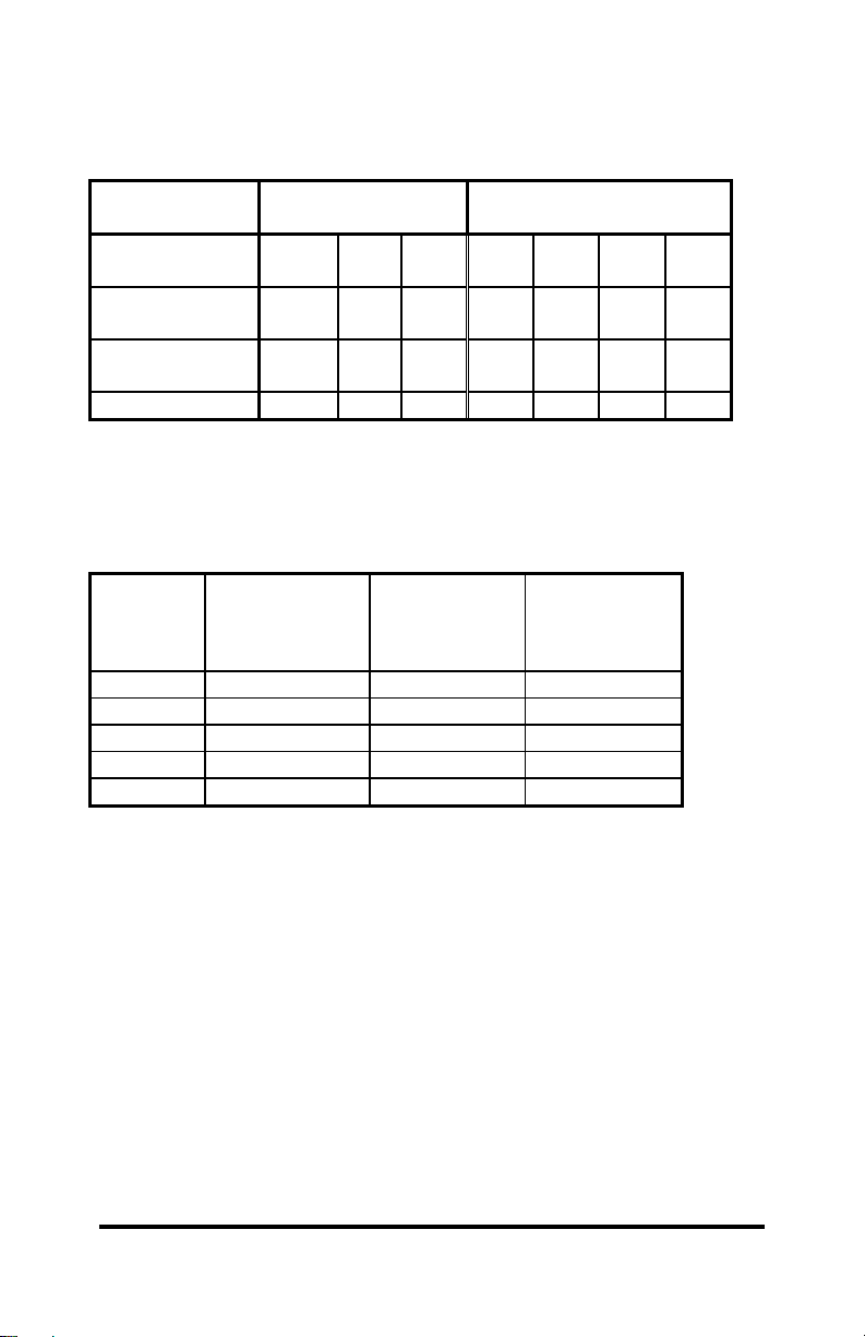
Table 1. Address Switches
1st Digit 2nd Digit
Switch
7 654321
Position
Bus
SA10 SA9 SA8 SA7 SA6 SA5 SA4
Connection
Decimal
1024 512 256 128 64 32 16
Weight
Hex Weight
400 200 100 80 40 20 10
To set the address of the 2IQEC2/4 card at some common
locations, follow the switch settings shown in Table 2.
Table 2. Frequently Unused Port Addresses
Base
Hex
Address
Binary
Equivalent
Switch
Settings
MSB LSB
I/O Space
Description
7654321
200 1000000000 0100000 game port
300 1100000000 0110000 prototype
310 1100010000 0110001 prototype
380 1110000000 0111000 SDLC
3A0 1110100000 0111010 bisync com
To install at another address, follow the procedure below.
1. Select the address. Using an I/O port usage table (one is
included in Appendix A) select an unused hex address
space. Note that the card occupies 16 bytes of I/O space.
Use caution when selecting a port address. It is very
important that nothing else is installed at the selected
address.
2. Convert the hex address to its binary equivalent.
3. Throw away the 4 least significant bits.
4. The remaining 7 digits represent the switch address. 1's
represent an OFF switch. 0's represent an ON switch.
4 2IQEC2/43798 Manual
B&B Electronics -- PO Box 1040 -- Ottawa, IL 61350
PH (815) 433-5100 -- FAX (815) 433-5105
Page 7
IRQ
The 2IQEC2/4 card allows the use of interrupts (IRQ) 2-7,
10-12, 14, and 15. This interrupt is shared with all the channels. To
determine the channel that caused the interrupt, the interrupt
service routine must read the address located at the base address
plus 8. The lower nibble will indicate which channel caused the
interrupt. Where bit 0 is the X-Axis, bit 1 is the Y-Axis, bit 2 is the ZAxis, and bit 3 is the W-Axis. The upper nibble is not used. To
clear the interrupt, the interrupt service routine must read or write to
the address located at base address plus 12 (0xC). The IRQ is set
by placing a jumper on JP1. Only one jumper should be placed on
JP1 at any one time. Check Table 3 for common interrupt uses.
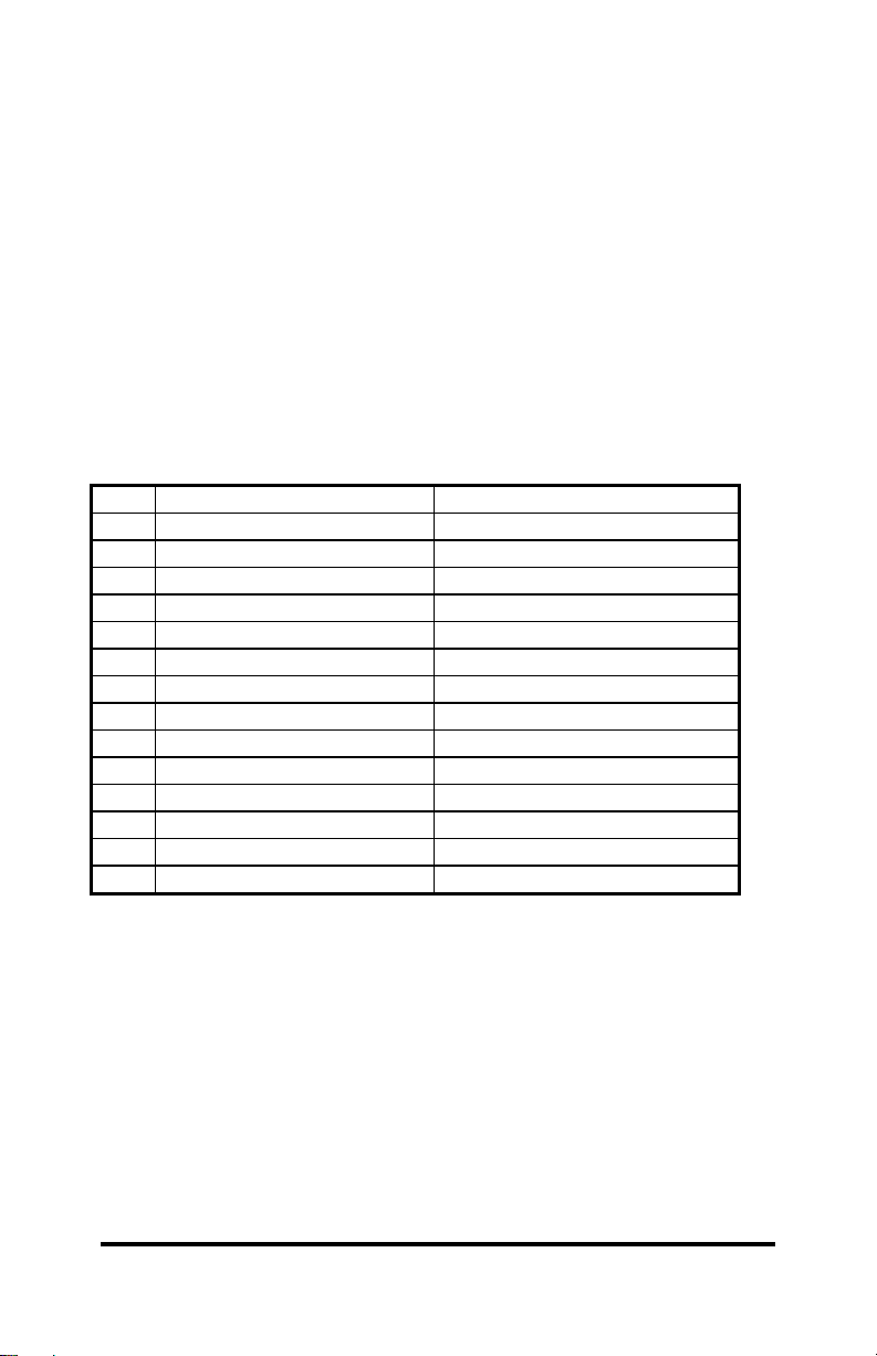
Table 3. Hardware Interrupts
IRQ AT machines XT machines
2 routed to IRQ controller 2 Reserved
3 serial port COM2,4 Serial port COM2,4
4 serial port COM1,3 Serial port COM1,3
5 LPT2 hard disk
6 floppy disk Floppy disk
7 LPT1 parallel printer port 1 (LPT1)
8 real-time clock not available
9 re-directed to IRQ2 not available
10 Unassigned not available
11 Unassigned not available
12 Unassigned not available
13 Coprocessor not available
14 hard disk not available
15 Unassigned not available
The conditions required to generate an interrupt can be
selected by the use of jumpers. Each axis is independently
configured. Note that more than one condition can be configured to
generate the interrupt. Note that the use of an interrupt is not
required.
2IQEC2/43798 Manual 5
B&B Electronics -- PO Box 1040 -- Ottawa, IL 61350
PH (815) 433-5100 -- FAX (815) 433-5105
Page 8

Configuring the jumpers
The jumpers located on the left side of the card make it
easy to configure the card to your individual needs. The jumpers
are grouped by axis and function. The top group of jumpers is for
the X axis. Then next groups going down are for the Y-axis, Z-axis,
and W-axis respectfully. There are three signals that can be routed
via these jumpers. They are the FLG1 and FLG2 outputs from the
counter chips, and the index from the encoder. The FLG1 and
FLG2 outputs are software configurable. The FLG1 can be
configured to act as a carry (pulse on counter overflow), compare
(pulse when counter equals the preset register), index, or carry and
borrow (pulse on either an overflow or an underflow of the counter).
The FLG2 can be configured to act as a borrow, up-down indicator,
or an error flag. These outputs are brought to the user connectors.
The first jumpers labeled JP4, JP8, JP12 and JP16 allow
you to select what conditions cause the counter to be loaded with
the preset value in the preset register. The middle jumpers labeled
JP3, JP7, JP11, and JP15 allow you to select what conditions cause
the counter to be reset or the counter to be enabled depending on
the software configuration of the input. The last jumpers labeled
JP2, JP6, JP10, and JP14 are used to define what conditions cause
an interrupt (IRQ).
JP5 selects the type of input encoder signals for the X and
Y axes not including the index. Set jumper JP5 for RS-422
differential mode and remove the jumper for TTL level encoder
input. When in differential mode the TTL output of the differential
receivers is present at the TTL pins. Leave these pins unconnected
in differential mode.
JP13 selects the type of input encoder signals for the Z and
W axis not including the index. Set jumper JP13 for RS-422
differential mode and remove the jumper for TTL level encoder
input. When in differential mode the TTL output of the differential
receivers is present at the TTL pins. Leave these pins unconnected
in differential mode.
JP9 selects the type of input from the index pins. This
jumper affects all the axes' index inputs. Set jumper JP9 for RS-422
differential mode and remove the jumper for TTL level encoder
input. When in differential mode the TTL output of the index
receivers is present at the TTL pins. Leave these pins unconnected
in differential mode.
6 2IQEC2/43798 Manual
B&B Electronics -- PO Box 1040 -- Ottawa, IL 61350
PH (815) 433-5100 -- FAX (815) 433-5105
Page 9

Location of Jumpers
2IQEC2/43798 Manual 7
B&B Electronics -- PO Box 1040 -- Ottawa, IL 61350
PH (815) 433-5100 -- FAX (815) 433-5105
Page 10

Software Registers
Flag Register (Read Data Address)
The FLAG register is a read-only register that holds the
status information of the counters and can be read out on the data
bus. To read the FLAG byte for any axis, read the control address
of that axis.
FLAG Byte Defined
76543210
BT: Borrow toggle flip-flop.
Toggles every time CNTR underflows
CT: Carry toggle flip-flop.
Toggles every time CNTR overflows
CPT: Compare toggle flip-flop.
Toggles every time PR equals CNTR.
S: Sign flag. Set to 1 whenCNTR underflows.
Reset to 0 when CNTR overflows
E: Error flag. Set to 1 when excessive noise is present at
the count inputs in quadrature mode. Irrelevant innonquadrature mode.
U/D': Up/Down flag. Set to 1 when counting up
And reset to 0 when counting down
IDX: Index. Set to 1 when selected index input is at active
level.
0: Not used. Always reset to 0.
Reset and Load Signal Decoders (Write to Control Address)
The following functions can be performed by writing to the
control address for that axis. Note that bits 5 and 6 define the
register and should always be zero when writing to the RLD register.
RLD Byte Defined
76543210
X00XXXX0NOP
X00XXXX1ResetBP
X00XX00XNOP
X 0 0 X X 0 1 X Reset CNTR
X 0 0 X X 1 0 X ResetBT,CT,CPT,S
X00XX11XResetE
X0000XXXNOP
X0001XXXTransferPRtoCNTR
X0010XXXTransferCNTRtoOL
X0011XXXTransferPR0toPSC
000XXXXXSelecttheRLDaddressed by X'/Y input
100XXXXXSelectbothXRLDandYRLDorZRLDandWRLDtogether
8 2IQEC2/43798 Manual
B&B Electronics -- PO Box 1040 -- Ottawa, IL 61350
PH (815) 433-5100 -- FAX (815) 433-5105
Page 11

Filter Clock Prescalers
Each PSC is an 8-bit programmable modulo-N down
counter, driven by the FCK clock. The factor N is downloaded into a
PSC from the associated PR low byte register PR0. The PSCs
provide the ability to generate independent filter clock frequencies
for each channel.
Final filter clock frequency
FFCKn=f
FCK/(n+1), where n=PSC=0 to 255
Counter Mode Registers (Write to Control Address)
The counter’s operational mode is programmed by writing a
byte into the counter mode registers (CMRs).
CMR Byte Defined
76543210
X01XXXX0BinaryCount
X01XXXX1BinaryCoded Decimal Count
X 0 1 X X 0 0 X Normal Count
X 0 1 X X 0 1 X Range Limit
X 0 1 X X 1 0 X Non-Recycle Count
X 0 1 X X 1 1 X Modulo-N
X0100XXXNon-quadrature
X0101XXXQuadrature 1X
X0110XXXQuadrature 2X
X0111XXXQuadrature 4X
001XXXXXSelecttheCMRaddressed by X'/Y input
101XXXXXSelectbothXCMRandYCMRorZCMRandWCMR
together
Definitions of count modes
Range Limit. In range limit count mode, an upper and a
lower limit is set, mimicking limit switches in the mechanical
counterpart. The upper limit is set by the contents of the PR and the
lower limit is set to be 0. The CNTR freezes at CNTR=PR when
counting up and at CNTR=0 when counting down. At either of these
limits, the counting is resumed only when the count direction is
reversed.
2IQEC2/43798 Manual 9
B&B Electronics -- PO Box 1040 -- Ottawa, IL 61350
PH (815) 433-5100 -- FAX (815) 433-5105
Page 12

Non-Recycle. In non-recycle count mode, the CNTR is disabled,
whenever a count overflow or underflow takes place. The end of
cycle is marked by the generation of a Carry (in Up Count) or a
Borrow (in Down Count). The CNTR is re-enabled when a reset or
load operation is performed on the CNTR.
Modulo-N. In modulo-N count mode, a count boundary is set
between 0 and the content of PR. When counting up at CNTR=PR,
the CNTR is reset to 0 and the up count is continued from that point.
When counting down, at CNTR=0, the CNTR is loaded with the
content of PR and down count is continued from that point.
The modulo-N is true bidirectional in that the divide-by-N
output frequency is generated in both up and down direction of
counting for same N and does not require the complement of N in
the UP instance. In frequency divider application, the modulo-N
output frequency can be obtained at either the Compare(FLG1) or
the Borrow(FLG2) output. Modulo-N output frequency, f
where f
I is the input count frequency and N=PR.
N=fI/(N+1)
Input/Output Control Register (Write to Control Address)
The functional modes of the programmable input and output
pins are written into the IORs.
IOR Byte Defined
76543210
X10XXXX0Disableinputs A and B
X10XXXX1Enable inputs A and B
X 1 0 X X X 0 X LCNTR'/LOL' pin is Load CNTR input
X 1 0 X X X 1 X LCNTR'/LOL' pin is Load OL input
X 1 0 X X 1 X X RCNTR'/ABG pin is Reset CNTR input
X 1 0 X X 0 X X RCNTR'/ABG pin is A and B Enable gate
X1000XXXFLG1pinisCarry'output,FLG2pinisBorrow'output
X1001XXXFLG1pinisCompare'output,FLG2pinisBorrow'output
X1010XXXFLG1pinisCarry'/Borrow'output,FLG2pinisU/D'
X1011XXXFLG1pinisIDX,FLG2isE
010XXXXXSelecttheIORaddressed by X'/Y input
110XXXXXSelectbothXIORandYIORorZIORandWIORtogether
10 2IQEC2/43798 Manual
B&B Electronics -- PO Box 1040 -- Ottawa, IL 61350
PH (815) 433-5100 -- FAX (815) 433-5105
Page 13

Index Control Registers (Write to Control Address)
Either the LCNTR'/LOL' or the RCNTR'/ABG inputs can be
initialized to operate as an index input. When initialized as such,
the index signal from the encoder, applied to one of these inputs
performs either the Reset CNTR or the Load CNTR or the Load OL
operation synchronously with the quadrature clocks. Note that only
one of these inputs can be selected as the Index input at a time and
hence only one type on indexing function can be performed in any
given set-up. The index function must be disabled in nonquadrature count mode.
IDR Byte Defined
76543210
X11XXXX0DisableIndex
X11XXXX1Enable Index
X 1 1 X X X 0 X Negative Index Polarity
X 1 1 X X X 1 X Positive Index Polarity
X 1 1 X X 1 X X LCNTR'/LOL' pin is indexed
X 1 1 X X 0 X X RCNTR'/ABG pin is indexed
011XXXXXSelecttheIDRaddressed by X'/Y input
111XXXXXSelectbothXCIDRandYIDRorZIDRandWIDRtogether
2IQEC2/43798 Manual 11
B&B Electronics -- PO Box 1040 -- Ottawa, IL 61350
PH (815) 433-5100 -- FAX (815) 433-5105
Page 14

Chapter 3:
If you are unable to communicate with the card from your software:
1. Double check that the address is properly set.
3. Check your pinouts.
4. Try the demo software that comes with the card.
5. Call B&B Electronics' Technical Support. Technicians are
available at (815) 433-5100 to answer your questions from 8
am - 5:00 pm weekdays (Central Time).
TROUBLESHOOTING
12 2IQEC2/43798 Manual
B&B Electronics -- PO Box 1040 -- Ottawa, IL 61350
PH (815) 433-5100 -- FAX (815) 433-5105
Page 15

Appendix A: Hardware I/O Map
I/O Map of XT Class Machines
Hex Address Address Function in XT Class Machines
000-00F DMA controller (8237A)
020-021 interrupt controller (8259A)
040-043 timer (8253)
060-063 PPI (8255A)
080-083 DMA page register (74LS612)
0A0-0AF NMI - non maskable interrupt
200-20F game port joystick controller
210-217 expansion unit
2E8-2EF COM4 serial port
2F8-2FF COM2 serial port
300-31F prototype card
320-32F hard disk
378-37F parallel printer
380-38F SDLC
3B0-3BF MDA - monochrome adapter and printer
3D0-3D7 CGA - color graphics adapter
3E8-3EF COM3 serial port
3F0-3F7 floppy diskette controller
3F8-3FF COM1 serial port
2IQEC2/43798 Manual Appendix A: Hardware I/O Maps A-1
B&B Electronics -- PO Box 1040 -- Ottawa, IL 61350
PH (815) 433-5100 -- FAX (815) 433-5105
Page 16

Hardware I/O Map of AT Class Machines
Hex Address Address Function in AT Class Machines
000-01F DMA controller #1 (8237A-5)
020-03F interrupt controller #1 (8259A)
040-05F timer (8254)
060-06F keyboard (8042)
070-07F NMI - non maskable interrupt & CMOS RAM
080-09F DMA page register (74LS612)
0A0-0BF interrupt controller #2 (8259A)
0C0-0DF DMA controller #2 (8237A)
0F0-0FF 80287 math coprocessor
1F0-1F8 hard disk
200-20F game port joystick controller
258-25F Intel Above Board
278-27F parallel printer port 2
2E8-2EF COM4 serial port
2F8-2FF COM2 serial port
300-31F prototype card
378-37F parallel printer 1
380-38F SDLC or bisynch com 2
3A0-3AF bisynch com 1
3B0-3BF MDA - monochrome adapter
3BC-3BE parallel printer on monochrome adapter
3C0-3CF EGA - reserved
3D0-3D7 CGA - color graphics adapter
3E8-3EF COM 3 serial port
3F0-3F7 floppy diskette controller
3F8-3FF COM1 serial port
Any sixteen byte space not listed above and not used
by any other equipment in your system may be used for the
serial port.
A-2 Appendix A: Hardware I/O Maps 2IQEC2/43798 Manual
B&B Electronics -- PO Box 1040 -- Ottawa, IL 61350
PH (815) 433-5100 -- FAX (815) 433-5105
Page 17

Appendix B: Specifications/Timing Diagrams
Pin Description
1. A+
2. A-
3. A (TTL)
4. B+
5. B-
6. B (TTL)
7. I+
8. I-
9. I (TTL)
10. FLG 2 (Programmed output)
11. FLG 1 (Programmed output)
12. Load Counter (Input)
13. Reset Counter (Input)
14. +5VDC
15. Ground
Addresses
Base .............................X Axis Data
Base+1 .........................X Axis Control
Base+2 .........................Y Axis Data
Base+3 .........................Y Axis Control
Base+4 .........................Z Axis Data
Base+5 .........................Z Axis Control
Base+6 .........................W Axis Data
Base+7 .........................W Axis Control
Base+8 .........................IRQ Register
Base+9 .........................Do not use
Base+10 .......................Do not use
Base+11 .......................Do not use
Base+12 .......................Clear IRQ
Base+13 .......................Do not use
Base+14 .......................Do not use
Base+15 .......................Do not use
2IQEC2/43798 Manual Appendix B: Specifications B-1
B&B Electronics -- PO Box 1040 -- Ottawa, IL 61350
PH (815) 433-5100 -- FAX (815) 433-5105
Page 18

Transient Characteristics
Quadrature Mode
Parameter Symbol Min.Value Max. Value Unit Remarks
FCK High Pulse Width t1 21 - ns FCK Low Pulse Width t
FCK Frequency f
Mod-n Filter Clock (FCKn)Period t
2 21 - ns -
FCK -24MHz-
3 42 - ns t3= (n+1) (t1+t2),
where
N=PSC=0 to FF
FCKn Frequency fFCKn -24MHzQuadrature Separation t
4 83 - ns t4≥2t3
Quadrature Clock Pulse Width t5 167 - ns t5≥4t3
Quadrature Clock Frequency fQA,fQB -3 MHzfQA=fQB=1/8t3
Quadrature Clock to Count Delay tQ1 5t3 6t3 --
X1/X2/X4 Count Clock Pulse Width t
Q2 42 - ns tQ2=t3
Index Input Pulse Width tidx 125 - ns tidx≥3t3
Index Skew from A tAi -42nstAi≤t3
Carry/Borrow/Compare Output Width tQ3 42 - ns tQ3=t3
Non-Quadrature Mode
Parameter Symbol Min.Value Max. Value Unit Remarks
Clock A – High Pulse Width t6 16 - ns -
Clock A – Low Pulse Width t
Direction Input B Set-up Time t
Direction Input B Hold Time t
Gate Input (ABG) Set-up Time t
Gate Input (ABG) Hold Time t
Clock Frequency (non-Mod-N) f
Clock Frequency (Mod-N) f
Clock to Carry or Borrow Out Delay t
Carry or Borrow Out Pulse Width t
Load CNTR, Reset CNTR and
Load OL Pulse Width t
Clock to Compare Out Delay t
7 16 - ns -
8S 20 - ns -
8H 20 - ns -
GS 20 - ns -
GH 20 - ns -
A -30MHzfA=(1/ (t6+t7))
AN -25MHz-
9 -30ns-
10 16 - ns t10=t7
11 20 - ns -
12 50 - ns -
H
B-2 Appendix B: Specifications 2IQEC2/43798 Manual
B&B Electronics -- PO Box 1040 -- Ottawa, IL 61350
PH (815) 433-5100 -- FAX (815) 433-5105
Page 19

Filter Clock (modulo-1 shown)
Quadrature Clock and Index (Positive index shown)
2IQEC2/43798 Manual Appendix B: Specifications B-3
B&B Electronics -- PO Box 1040 -- Ottawa, IL 61350
PH (815) 433-5100 -- FAX (815) 433-5105
Page 20

Carry, Borrow, Compare, Carry Toggle, Borrow Toggle and
Compare Toggle
(4X Quadrature, Normal, Binary Count, and PR=1)
Non Quadrature mode (A=Count B=Direction)
B-4 Appendix B: Specifications 2IQEC2/43798 Manual
B&B Electronics -- PO Box 1040 -- Ottawa, IL 61350
PH (815) 433-5100 -- FAX (815) 433-5105
Page 21

Non-Recycle, Non-Quadrature, BCD Mode
Modulo-N, Non-Quadrature (Modulo-3 shown)
Range Limit, Non-Quadrature (PR=4)
2IQEC2/43798 Manual Appendix B: Specifications B-5
B&B Electronics -- PO Box 1040 -- Ottawa, IL 61350
PH (815) 433-5100 -- FAX (815) 433-5105
Page 22

Appendix C: Typical Set-up Examples
2IQEC2/43798 Manual Appendix C: Typical Set-up Examples C-1
B&B Electronics -- PO Box 1040 -- Ottawa, IL 61350
PH (815) 433-5100 -- FAX (815) 433-5105
 Loading...