

Page 1

RS-232 Digital I/O Module
Model 232SDD16
Documentation Number 232SDD16-1005
Designed and Manufactured
In Ottawa, Illinois
of domestic and imported parts by
B&B Electronics Mfg. Co. Inc.
707 Dayton Road -- P.O. Box 1040 -- Ottawa, IL 61350
PH (815) 433-5100 -- FAX (815) 433-5104
http://www.bb-elec.com
sales@bb-elec.com
support@bb.elec.com
1995 B&B Electronics -- Revised February 2005
pn#3604-r1
This product
USA
Internet:
232SDD16-1005 Manual Cover Page
B&B Electronics -- PO Box 1040 -- Ottawa, IL 61350
PH (815) 433-5100 -- FAX (815) 433-5104
Page 2

Table of Contents
Chapter 1- Introduction........................................... 1
232SDD16 Features............................................... 1
Packing List............................................................2
232SDD16 Specifications....................................... 3
I/O Lines................................................................................3
Digital Inputs......................................................................3
Digital Outputs...................................................................3
Power Supply........................................................................3
Communications ...................................................................3
Size .......................................................................................3
Chapter 5 - Software.............................................. 21
Programming Techniques.....................................21
Read I/O States Command.................................................21
Read Configurat ion Command ...........................................22
Set Output States Command..............................................24
Define I/O Lines Command.................................................25
Set Power-up States Command .........................................25
Demonstration Program ....................................... 27
Hard Drive Installation .......... Error! Bookmark not defined.
Running Demonstration Program .......................................27
APPENDIX A..........................................................A-1
ASCII Character Codes.......................................A-1
Chapter 2 - Connections......................................... 5
Digital I/O Connections........................................... 5
Digital Inputs ..... ....................................................................5
Digital Outputs.......................................................................5
Ground ..................................................................................5
Serial Port Connections.......................................... 6
Power Supply Connections..................................... 8
Chapter 3 - Commands........................................... 9
Syntax .................................................................. 10
I/O Data Bytes...... .............................. .................................10
Read I/O Lines Command.................................... 12
Set Output Lines Command................................. 12
Define I/O Lines Command..................................13
Set Power-up States Command........................... 14
Read Configuration Command............................. 14
Chapter 4 - I/O Interfacing..................................... 17
Digital Inputs......................................................... 17
Digital Outputs...................................................... 19
APPENDIX B..........................................................B-1
Hexadecimal/Decimal Conversions.....................B-1
APPENDIX C..........................................................C-1
Interface Modules for SDD16 Models..................C-1
DTB25.................................................................C-2
DBM16 ................................................................C-4
DBM16 Interfacing ............................................................C-5
Inputs.............................................................................C-5
Outputs..........................................................................C-7
DBM16 Specificat ions.......................................................C-9
I/O Lines ........................................................................C-9
Inputs.................................................................................C-9
Outputs..............................................................................C-9
Power Supply ................................................... .............C-9
Size................................................................................C-9
APPENDIX D.......................................................D-1
Adding Data Field Confirmation...........................D-1
232SDD16-1005 Manual Table of Contents i
B&B Electronics -- PO Box 1040 -- Ottawa, IL 61350
PH (815) 433-5100 -- FAX (815) 433-5104
ii Table of Contents 232SDD16-1005 Manual
B&B Electronics -- PO Box 1040 -- Ottawa, IL 61350
PH (815) 433-5100 -- FAX (815) 433-5104
Page 3
Chapter 1- Introduction
232SDD16 Features
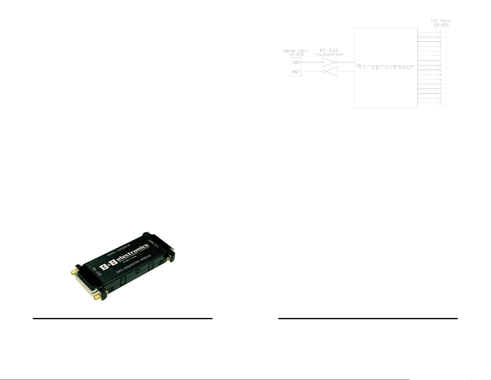
The 232SDD16 is a general purpose control module that is
connected to your computer’s RS-232 serial port. The 232SDD16
offers 16 discrete digital I/O lines. With these features, the module
can be used to sense external ON/OFF conditions and to control a
variety of devices.
The digital outputs are CMOS/TTL compatible. The digital inputs
are CMOS/TTL compatible. The digital I/O lines are available
through a DB-25S (female) connector.
The 232SDD16 connects to your computer’s RS-232 serial port
through a DB-25S connector. The unit automatically detects baud
rates from 1200 to 9600. A data format of 8 data bits, 1 stop bit and
no parity is used.
Configuration parameters are stored in non-volatile memory.
The configuration parameters consists of I/O definitions, and output
power-up states.
The unit may be powered by setting RTS and DTR high on the
serial port. If the 232SDD16 cannot be powered using the
handshake lines, it may be powered with +12Vdc through the 2.5mm
jack or through the DB-25 I/O connector.
NOTE: When using an external supply, the supply should be
connected only to specifically labeled power inputs (power
jack, terminal block, etc.). Connecting an external power supply
to the handshake lines may damage the unit. Contact technical
support for more information on connecting an external power
supply to the handshake lines.
Figure 1.2 - Simplified Block Diagram
Packing List
Examine the shipping carton and contents for physical damage.
The following items should be in the shipping carton:
1. 232SDD16 unit
2. Software
3. This instruction manual
If any of these items are damaged or missing contact B&B
Electronics immediately.
Figure 1.1 - 232SDD16 Module
232SDD16-1005 Manual 1
B&B Electronics -- PO Box 1040 -- Ottawa, IL 61350
PH (815) 433-5100 -- FAX (815) 433-5104
2 232SDD16-1005 Manual
B&B Electronics -- PO Box 1040 -- Ottawa, IL 61350
PH (815) 433-5100 -- FAX (815) 433-5104
Page 4

232SDD16 Specifications
I/O Lines
Total: 16 (Factory default = inputs)
Digital Inputs
Voltage Range: 0 Vdc to 5 Vdc
Low Voltage: 1.0 Vdc max.
High Voltage: 2.0 Vdc min.
Leakage Current: 1 microamp max.
Digital Outputs
Low Voltage: 0.6 Vdc @ 8.3 milliamps (Sink)
High Voltage: 4.3 Vdc @ -3.1 milliamps (Source)
Power Supply
Input Voltage: 8 Vdc to 16 Vdc
External power: 35 milliamps* @ 12Vdc
Port power: 15 milliamps* (The RS-232 RTS
and DTR lines must be high to port
power unit.)
Doesn’t include the power consumption of external devices.
Communications
Standard: RS-232 (unit is DCE)
Baud Rate: 1200 to 9600 (automatic detection)
Format: 8 data bits, 1 stop bit, no parity
Connector: DB25S (female)
Size 0.7" x 2.1" x 4.7"
232SDD16-1005 Manual 3
B&B Electronics -- PO Box 1040 -- Ottawa, IL 61350
PH (815) 433-5100 -- FAX (815) 433-5104
4 232SDD16-1005 Manual
B&B Electronics -- PO Box 1040 -- Ottawa, IL 61350
PH (815) 433-5100 -- FAX (815) 433-5104
Page 5
Chapter 2 - Connections
This chapter will cover the connections required for the
232SDD16. There are three sets of connections: digital I/O, serial
port, and power supply. Do not make any connections to the
232SDD16 until you have read this chapter.
Digital I/O Connections
Connections to the I/O lines are made through the DB25S
(female) I/O port connector. Refer to Table 2.1. See Chapt er 5 for
I/O interfacing examples.
Digital Inputs
The digital input lines are CMOS/TTL compatible and can handle
voltages from 0Vdc to +5Vdc.
Digital Outputs
The digital output lines have a maximum voltage of +5Vdc and
are CMOS/TTL compatible.
Ground
The pin should be connected to your external digital devices
ground.
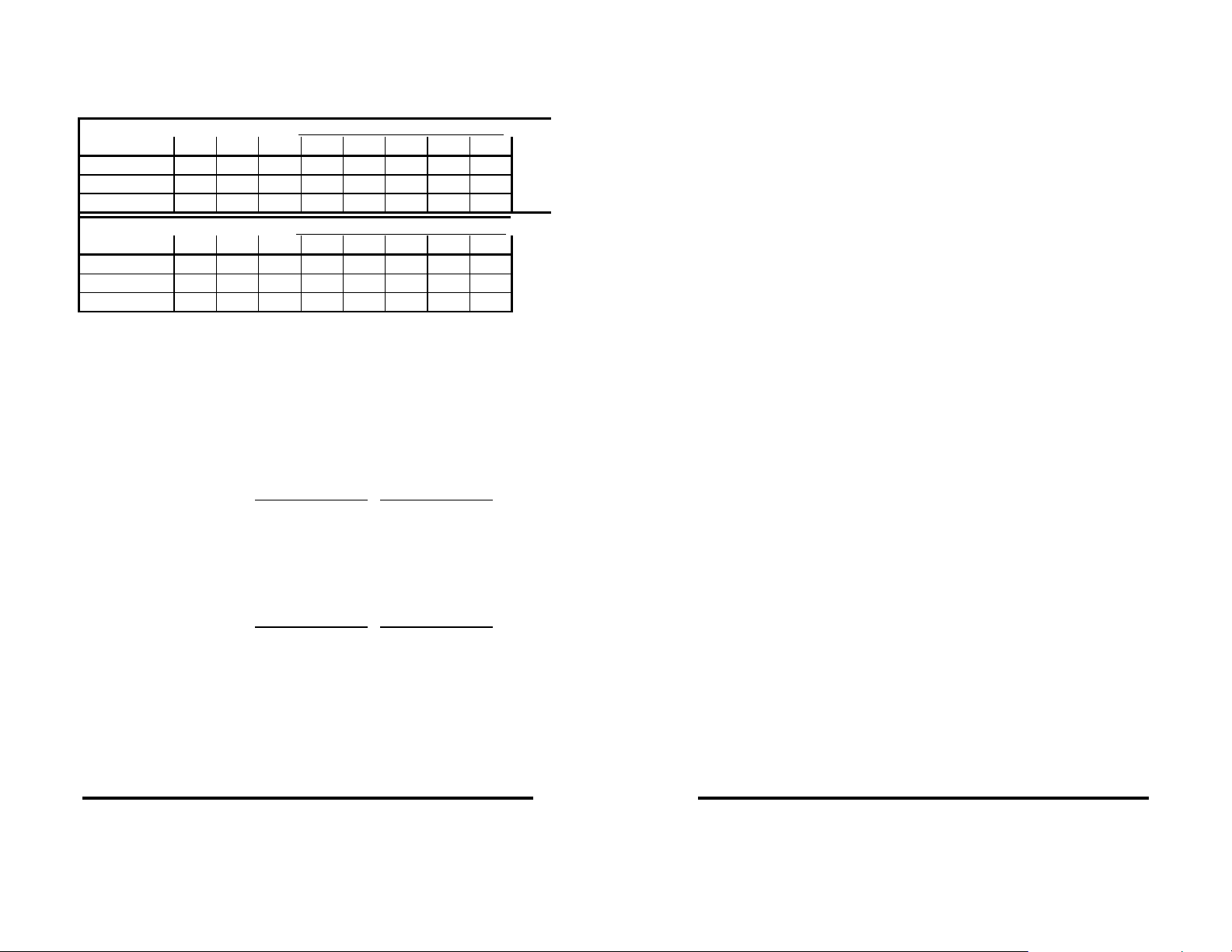
Table 2.1 - 232SDD16 I/O Port Pinout
DB-25S
Pin #
10 I/O #1 23 I/O #7
11 I/O #2 24 I/O #6
12 I/O #3 25 I/O #5
13 I/O #4
Function
1 No connection 14 I/O #15
2 No connection 15 I/O #14
3 No connection 16 I/O #13
4 No connection 17 I/O #12
5 No connection 18 I/O #11
6 No connection 19 I/O #10
7 Ground 20 No connection
8 +12Vdc Input 21 I/O #9
9 I/O #0 22 I/O #8
DB-25S
Pin #
Function
Serial Port Connections
In order to communicate to the 232SDD16 module it must be
connected to an RS-232 serial port. The unit automatically detects
baud rates from 1200 to 9600. A data format of 8 data bits, 1 stop
bit and no parity is used.
device (See Table 2.2). If your communications equipment is
configured as a DTE device, such as a standard IBM PC serial port,
the 232SDD16 should be connected using a “straight through” DB25 cable or a standard DB-9 to DB-25 cable adapter as shown in
Table 2.3. If your communications equipment is configured as a
DCE device, such as a modem, the 232SDD16 should be connected
using a “null modem” cable (See Table 2.4).
The 232SDD16 is configured as a DCE
232SDD16-1005 Manual 5
B&B Electronics -- PO Box 1040 -- Ottawa, IL 61350
PH (815) 433-5100 -- FAX (815) 433-5104
6 232SDD16-1005 Manual
B&B Electronics -- PO Box 1040 -- Ottawa, IL 61350
PH (815) 433-5100 -- FAX (815) 433-5104
Page 6
Table 2.2 - RS-232 Connector Pinout
DB-25S
Pin #
Signal
Signal
Direction at
232SDD16
Notes
2 Transmit Data (TD) Input Connection is required.
3 Receive Data (RD) Output Connection is required.
4 Request to Send
(RTS)
Input May be used to power
unit if kept high.
7 Signal Ground (SG) Connection is required.
20 Data Terminal
Ready (DTR)
Input May be used to power
unit if kept high.
Table 2.3 - 232SDD16 To DTE Connections
232SDD1
6 Pin #
Signal
DTE DB-
25
Connection
2 Transmit Data (TD) 2 3
3 Receive Data (RD) 3 2
4 Request to Send (RTS) 4 7
7 Signal Ground (SG) 7 5
20 Data Terminal Ready (DTR) 20 4
DTE DB-9
Connection
Table 2.4 - 232SDD16 To DCE Connections
232SDD16
Pin #
2 Transmit Data (TD) 3 2
3 Receive Data (RD) 2 3
4 Request to Send (RTS) 5 8
7 Signal Ground (SG) 7 5
20 Data Terminal Ready
(DTR)
Signal
DCE DB-25
Connection
DCE DB-9
Connection
6 6
Power Supply Connections
Power to the 232SDD16 can be supplied by the RS-232 serial
port handshake lines (RTS, DTR) or by an external power supply
through the 2.5mm power jack or from the I/O connector. Most serial
ports can provide enough power to supply the 232SDD16’s 15
milliamp requirement. If you plan to use this method to power the
unit, your software must set the RS-232 RTS and DTR lines to the
high state. An external power supply must be able to supply 8 to 16
Vdc at 35ma.
NOTE: Power requirements of the module does not include the
power consumption of any external devices connected to the
module. Therefore, any current that is sourced by the digital outputs
must be added to this value and the current must not exceed the
maximum output source current. Refer to the 232SDD16
Specification Section of this manual.
232SDD16-1005 Manual 7
B&B Electronics -- PO Box 1040 -- Ottawa, IL 61350
PH (815) 433-5100 -- FAX (815) 433-5104
8 232SDD16-1005 Manual
B&B Electronics -- PO Box 1040 -- Ottawa, IL 61350
PH (815) 433-5100 -- FAX (815) 433-5104
Page 7
Chapter 3 - Commands
There are only two commands required to control the 232SDD16:
set output lines, and read I/O lines. Three additional commands are
used for configuring the module: define I/O lines, set power-up
states, and read configuration. Command strings are from four to
six bytes in length; the “!” character, the “0” (zero) character, two
command characters, and one or two data bytes, if required. (See
Table 3.1).
Table 3.1 - 232SDD16 Commands
Function Command Response
Set Output Lines !0SO{I/O msb}{I/O lsb} no response
Read I/O Lines !0RD {I/O msb}{I/O lsb}
Define I/O Lines !0SD{I/O msb}{I/O lsb} no response
Set Power-up States !0SS{I/O msb}{I/O lsb} no response
Read Configuration !0RC
Symbols: {...} represents one byte
<...> represents a numeric value
Before going into the specifics of each command, it is important
to understand that a byte has a numeric value from 0 to 255. The
byte's value can be represented in decimal (0 -255) format,
hexadecimal (00 - FF) format, binary (00000000 - 11111111) format
or as an ASCII character. The fixed bytes of each command will be
represented as ASCII chara cters, for example: “!0RD”. Refer to
Table 3.1. However, it is important to remember that an ASCII
character has a numeric value. Example: the ASCII “0” (zero) does
not have a value of zero but has a value of 48. The decimal and
hexadecimal equivalents of some ASCII characters are shown in
Table 3.2. Some commands require additional data bytes to
complete the command. These data bytes may be represented in
any of the formats listed above. Refer to Appendix A for more ASCII
and decimal equivalents.
I/O Definitions
{I/O msb}{I/O lsb}
Power-up States
{I/O msb}{I/O msb}
Table 3.2 - Equivalent Values
ASCII Decimal Hexadecimal
! 33 21h
0 48 30h
C 67 43h
D 68 44h
O 79 4Fh
R 82 52h
S 83 53h
Syntax
Command strings consists of four to six bytes. The first byte is
the start of message byte. The start of message byte is always the
ASCII “!” character. The second byte is the address byte. This byte
allows each unit to have a unique address (useful in RS-485
networks). Since the 232SDD16 uses RS-232 communications, this
byte is always the ASCII “0” character and can not be changed. The
next two bytes are the command characters. These bytes are ASCII
characters and used to specify which command will be executed by
the module. Some commands require an argument field. This field
contains the fifth and sixth data byte, a Most Significant and a Least
Significant data byte respectively.
Command Syntax: ! 0 _ _ _ _
| | | | | |
| | | | | 6th Data Byte
| | | | 5th Data Byte
| | | 2nd Command Byte
| | 1st Command Byte
| Address Byte
Start of Message Byte
I/O Data Bytes
When constructing commands to manipulate outputs lines or
when reading the state of the I/O lines it is necessary to know how
to select and interpret the I/O data bytes. The sixteen I/O lines are
represented by two data bytes. The Most Significant data byte
represents I/O lines #15 through #8 and the Least Significant data
byte represents I/O lines #7 through #0. The Most Significant byte is
always sent and received first followed by the Least Significant byte.
232SDD16-1005 Manual 9
B&B Electronics -- PO Box 1040 -- Ottawa, IL 61350
PH (815) 433-5100 -- FAX (815) 433-5104
10 232SDD16-1005 Manual
B&B Electronics -- PO Box 1040 -- Ottawa, IL 61350
PH (815) 433-5100 -- FAX (815) 433-5104
Page 8
A byte represents an eight-bit binary number (11111111),
therefore each byte can represent eight I/O lines. Each bit is
assigned a bit position and a weight (value). Refer to Table 3.3.
Table 3.3 - Bit Assignments for I/O Lines
MOST SIGNIFICANT I/O BYTE
I/O Line # 15 14 13 12 11 10 9 8
Bit Position 7 6 5 4 3 2 1 0
Hex Weight 80 40 20 10 8 4 2 1
Dec. Weight 128 64 32 16 8 4 2 1
LEAST SIGNIFICANT I/O BYTE
I/O Line # 7 6 5 4 3 2 1 0
Bit Position 7 6 5 4 3 2 1 0
Hex Weight 80 40 20 10 8 4 2 1
Dec. Weight 128 64 32 16 8 4 2 1
To set an output to a HIGH state the corresponding bit position
must be set to a "1". Conversely to set an output LOW the
corresponding bit position must be set to a "0". When reading I/O
lines, any bit set to a "0" indicates the corresponding I/O line is in
the LOW state and any bit set to a "1" indicates the corresponding
I/O line is in the HIGH state.
Example 3.1 - To set outputs 15, 8, 1, and 0 to a HIGH stat e, and all
other outputs to a LOW state (shown in bold face) -
MS Byte LS Byte
Shown in binary - 10000001 00000011
Shown in decimal - 129
(128+1)
Shown in hexadecimal - 81
(80h+1h)
Example 3.2 - Reply from Read I/O command (shown in bold face) -
MS Byte LS Byte
Shown in binary - 11001000 01010010
Shown in decimal - 200
(128+64+8)
Shown in hexadecimal - C8
(80h+40h+8h)
I/O lines #15, 14, 11, 6, 4, 1 are HIGH. All other I/O lines are LOW.
3
(2+1)
3
(2h+1h)
82
(64+16+2)
52
(40h+10h+2h)
Read I/O Lines Command
The Read I/O Lines command returns two data bytes that reflect
the state of the I/O lines. The first data byte contains the most
significant I/O lines (15 - 8). The second data byte contains the
least significant I/O lines (7 - 0). If a bit is a "0" then the state of that
I/O line is LOW. If a bit is a "1" then the state of that I/O line is HIGH.
Command: !0RD
Argument: none
Response: the state of the 16 I/O lines in two 8 bit bytes (shown in
bold face)
ASCII Example: !0RDÈR
Dec. Example: !0RD<200><82>
Hex. Example: !0RD<C8><52>
Bin. Example: !0RD<11001000><01010010>
Description: the first byte indicates that I/O lines #15, 14, & 11 are
HIGH and I/O lines # 13, 12, 10, 9, & 8 are LOW; the second byte
indicates that I/O lines # 6, 4, & 1 are HIGH and I/O lines # 7, 5, 3, 2,
& 0 are LOW.
Set Output Lines Command
The Set Output Lines command is used to set the states of the
output lines. This command requires two data bytes. These data
bytes specify the output state of each output line. The first data byte
represents the most significant I/O lines (15 - 8). The second data
byte represents the least significant I/O lines (7 - 0). If a bit posit i on
is set to a "0" then the state of that output line will be set LOW. If a
bit position is set to a "1" then the state of that output line will be set
HIGH.
NOTE: Refer to the "Define I/O Lines" command to define an I/O l ine
as an output.
232SDD16-1005 Manual 11
B&B Electronics -- PO Box 1040 -- Ottawa, IL 61350
PH (815) 433-5100 -- FAX (815) 433-5104
12 232SDD16-1005 Manual
B&B Electronics -- PO Box 1040 -- Ottawa, IL 61350
PH (815) 433-5100 -- FAX (815) 433-5104
Page 9

Command: !0SO
Argument: {I/O msb}{I/O lsb}
Response: none
ASCII Example: !0SOUA
Dec. Example: !0SO<85><65>
Hex. Example: !0SO <55><41>
Bin. Example: !0SO<01010101><01000001>
Description: the first byte sets output lines #14, 12, 10, & 8 HIGH
and output lines #15, 13, 11, & 9 LOW; the second byte sets output
lines #6, & 0 HIGH and output lines # 7, 5, 4, 3, 2, & 1 LOW. Note: If
any of these lines are defined as inputs the bit settings are ignored.
Define I/O Lines Command
The Define I/O Lines command is used to define each of the 16
I/O lines as either an input or an output. This command requires two
data bytes. Each data byte defines eight I/O lines. The first data
byte defines the eight most significant I/O lines (15 - 8). The second
data byte defines the eight least significant digital I/O lines (7 - 0). If
a bit position is set to a "0" then the I/O line will defined as an input.
If a bit position set to a "1" then the I/O line will be defined as an
output.
Command: !0SD
Argument: {I/O msb}{I/O lsb}
Response: none
ASCII Example: !0SDUA
Dec. Example: !0SD<85><65>
Hex. Example: !0SD<55><41>
Bin. Example: !0SD<01010101><01000001>
Description: the first byte define I/O lines #14, 12, 10, & 8 as
outputs and I/O lines #15, 13, 11, & 9 as inputs; the second byte
define I/O lines #6, & 0 as outputs and I/O lines #7, 5, 4, 3, 2, & 1 as
inputs.
Set Power-up States Command
The Set Power-up States command is used to set the states of
output lines when the module's power is recycled. This command
requires two data bytes. These data bytes specify the output state
of each output line. The first data byte represents the eight most
significant I/O lines (15 - 8). The second data byte represents the
eight least significant I/O lines (7 - 0). If a bit position is set to a "0"
then the state of that output line will be set LOW. If a bit position is
set to a "1" then the state of that output line will be set HIGH.
Command: !0SS
Argument: {I/O msb}{I/O lsb}
Response: none
ASCII Example: !0SSÛ@
Dec. Example: !0SS<219><64>
Hex. Example: !0SS<DB><40>
Bin. Example: !0SS<11011011><10000000>
Description: the first byte sets output lines #15, 14, 12, 11, 9, & 8
HIGH and output lines #13, & 10 LOW at power-up; the second byte
sets output line #7 HIGH and output lines #6, 5, 4, 3, 2, 1, & 0 LOW
at power-up. Note: If any of these lines are defined as inputs the bit
settings are ignored.
Read Configuration Command
The Read Configuration command returns the module's I/O
definitions and the outputs power-up state. Four data byt es are
returned. The first two data bytes contain the definition of th e eight
most significant I/O lines (15 - 8) and the eight least significant I/O
lines (7 - 0) respectively. If a bit position is set to a "0" the I/O line is
defined as an input, if set to a "1" the I/O line is defined as an output.
The second two data bytes contain the power-up states of the most
significant output lines (15 - 8) and the least significant output lines
(7 - 0) respectively. If a bit position is set to a "0" the power-up state
of the output will be LOW, if set to a "1" the output will be HIGH.
232SDD16-1005 Manual 13
B&B Electronics -- PO Box 1040 -- Ottawa, IL 61350
PH (815) 433-5100 -- FAX (815) 433-5104
14 232SDD16-1005 Manual
B&B Electronics -- PO Box 1040 -- Ottawa, IL 61350
PH (815) 433-5100 -- FAX (815) 433-5104
Page 10

Command: !0RC
Argument: none
Response: definition of the sixteen I/O lines in two 8 bit bytes, and
the power-up states in two 8 bit bytes. (shown in bold face)
ASCII Example: !0RCUAP@
Dec. Example: !0RC<85><65><80><64>
Hex. Example: !0RC<55><41><50><40>
Bin. Example: !0RC<01010101><01000001><01010000><01000000>
Description: the first byte (MSB of I/O definitions) - I/O lines #14, 12,
10, & 8 are outputs and I/O lines #15, 13, 11, & 9 are inputs; the
second byte (LSB of I/O definitions) - I/O lines #6, & 0 are outputs
and I/O lines #7, 5, 4, 3, 2, & 1 are inputs; the t hird byt e (MS B of
output power-up states) - output lines #14, & 12 HIGH and output
lines #10, & 8 LOW at power-up; the fourth byte (LSB of output
power-up states) - output line #6 HIGH and output line #0 LOW at
power-up.
232SDD16-1005 Manual 15
B&B Electronics -- PO Box 1040 -- Ottawa, IL 61350
PH (815) 433-5100 -- FAX (815) 433-5104
16 232SDD16-1005 Manual
B&B Electronics -- PO Box 1040 -- Ottawa, IL 61350
PH (815) 433-5100 -- FAX (815) 433-5104
Page 11

Chapter 4 - I/O Interfacing
This chapter will explain "HIGH" and "LOW" states and show
some general examples of how to interface to the I/O lines. Caution
must be taken not to exceed 232SDD16 specifications listed in
Chapter 1 when interfacing to external devices. Failure to stay
within these specifications could result in damage to the unit and will
void warranty.
Digital Inputs
As stated earlier, digital input lines are CMOS/TTL compatible
and can only handle voltages from 0Vdc to +5Vdc.
Digital inputs are used to sense a HIGH or a LOW state. This
can be accomplished via switch closures, contact closures, or a
solid state digital signal. When an I/O line, defined as an input,
senses a voltage level above +2.0Vdc it will be considered "HIGH"
and its input state will be read as a "1". Conversely, when an input
senses a voltage level below +1.0Vdc it will be considered "LOW"
and its input state will be read as a "0".
Inputs can also be used to sense AC voltages by using
mechanical or solid state relays. Solid state relays are available
from many manufacturers.
Figures 4.1 - 4.4 show examples of some typical input interfaces.
Figure 4.2 - Solid State Input
Figure 4.1 - Switch Input
232SDD16-1005 Manual 17
B&B Electronics -- PO Box 1040 -- Ottawa, IL 61350
PH (815) 433-5100 -- FAX (815) 433-5104
Figure 4.3 - Isolated Mechanical Input
18 232SDD16-1005 Manual
B&B Electronics -- PO Box 1040 -- Ottawa, IL 61350
PH (815) 433-5100 -- FAX (815) 433-5104
Page 12

Figure 4.4 - Isolated Solid State Input
Digital Outputs
Digital outputs are used to turn external devices on or off. Digital
outputs are CMOS/TTL compatible and operate between 0Vdc and
+5Vdc. Outputs can be used to control solid state output modules,
CMOS and TTL logic circuits. Caution must be taken not to exceed
the power capability of the outputs. Refer to the output
specifications in Chapter 1.
Setting an output line to a "1" forces the output HIGH, and setting
an output line to a "0" forces the output LOW.
Figures 4.5 - 4.6 show examples of some typical output
interfaces.
Figure 4.6 - Isolated Solid State Output
Figure 4.5 - Solid State Output
232SDD16-1005 Manual 19
B&B Electronics -- PO Box 1040 -- Ottawa, IL 61350
PH (815) 433-5100 -- FAX (815) 433-5104
20 232SDD16-1005 Manual
B&B Electronics -- PO Box 1040 -- Ottawa, IL 61350
PH (815) 433-5100 -- FAX (815) 433-5104
Page 13

Chapter 5 - Software
This chapter will be divided into two sections. The first section
covers programming techniques for constructing a command string,
receiving data and manipulating data in QuickBASIC. The second
section discusses how to install and run the demonstration program
on an IBM PC or compatible.
Programming Techniques
This section shows steps and examples of programming the
232SDD16 in QuickBasic. If you are programming in another
language, this section can be helpful as a guideline for programming
the 232SDD16.
Read I/O States Command
Step 1 - Constructing the command string:
Cmnd$ = "!0RD"
Step 2 - Transmitting the command string:
PRINT #1, Cmnd$;
Step 3 - Receiving the data:
MSIO$ = INPUT$(1,#1)
LSIO$ = INPUT$(1,#1)
Step 4 - Manipulating the data:
MSIO = ASC(MSIO$)
LSIO = ASC(LSIO$)
Step 5 - Determining an I/O's status:
MSstatus = MSIO AND mask
LSstatus = LSIO AND mask
By "ANDing" the value of MSIO or LSIO with the appropriate
mask of an I/O line, the status of the I/O line can be determined.
If the status is equal to zero the I/O line is LOW. If the status is
not equal to zero the I/O line is HIGH. Table 5.1 shows the mask
values for each I/O line.
Step 6 - Repeat Step 5 until the status of each I/O line has been
determined.
232SDD16-1005 Manual 21
B&B Electronics -- PO Box 1040 -- Ottawa, IL 61350
PH (815) 433-5100 -- FAX (815) 433-5104
Example 5.1 - Determining the status of I/O lines #2 & #10
mask = &H4
Cmnd$ = "!0RD"
PRINT #1, Cmnd$;
MSIO$ = INPUT$(1,#1)
LSIO$ = INPUT$(1,#1)
MSIO = ASC(MSIO$)
LSIO = ASC(LSIO$)
MSstatus = MSIO AND mask
LSstatus = LSIO AND mask
If LSstatus equals zero then I/O line #2 is LOW. If LSstatus is not
equal to zero then I/O line #2 is HIGH. If MSstatus equals zero then
I/O line #10 is LOW. If MSstatus is not equal to zero then I/O line
#10 is HIGH.
Table 5.1 - Digital I/O Mask Values
Mask Values
I/O Line # Hexadecimal Decimal
0 & 8 1H 1
1 & 9 2H 2
2 & 10 4H 4
3 & 11 8H 8
4 & 12 10H 16
5 & 13 20H 32
6 & 14 40H 64
7 & 15 80H 128
Read Configuration Command
Step 1 - Constructing the command string:
Cmnd$ = "!0RC"
Step 2 - Transmitting the command string:
PRINT #1, Cmnd$;
Step 3 - Receiving the data:
MSdefs$ = INPUT$(1,#1)
LSdefs$ = INPUT$(1,#1)
MSpups$ = INPUT$(1,#1)
LSpups$ = INPUT$(1,#1)
Step 4 - Manipulating the data:
MSdefs = ASC(MSdefs$)
LSdefs = ASC(LSdefs$)
MSpups = ASC(MSpups$)
LSpups = ASC(LSpups$)
22 232SDD16-1005 Manual
B&B Electronics -- PO Box 1040 -- Ottawa, IL 61350
PH (815) 433-5100 -- FAX (815) 433-5104
Page 14

Step 5 - Determining the I/O line definitions:
MSdefs = MSdefs AND mask
LSdefs = LSdefs AND mask
By "ANDing" the value of MSdefs or LSdefs with the appropriate
mask of an I/O line, the I/O line definition can be determined. If
the status is equal to zero the I/O line is an INPUT. If the status is
not equal to zero the I/O line is an OUTPUT. Table 5.1 shows
the mask values for each I/O line.
Step 6 - Repeat Step 5 until the status of each I/O line has been
determined.
Step 7 - Determining an OUTPUT's Power-up state:
MSpups = MSpups AND mask
LSpups = LSpups AND mask
By "ANDing" the value of MSpups or LSpups with the
appropriate mask of an Output line, the Output line definitio n can
be determined. If the status is equal to zero the Output power-up
state will be LOW. If the status is not equal to zero the Output
power-up state will be HIGH. Table 5.1 shows the mask values
for each I/O line.
Step 8 - Repeat Step 7 until the power-up state of each Output line
has been determined.
Example 5.2 - Determining the definition and power-up state of I / O
lines #2 & #10
mask = &H4
Cmnd$ = "!0RC"
PRINT #1, Cmnd$;
MSdefs$ = INPUT$(1,#1)
LSdefs$ = INPUT$(1,#1)
MSpups$ = INPUT$(1,#1)
LSpups$ = INPUT$(1,#1)
MSdefs = ASC(MSdefs$)
LSdefs = ASC(LSdefs$)
MSpups = ASC(MSpups$)
LSpups = ASC(LSpups$)
MSdefs = MSdefs AND mask
LSdefs = LSdefs AND mask
MSpups = MSpups AND mask
LSpups = LSpups AND mask
If LSdefs equals zero then I/O line #2 is an INPUT and if not equal
to zero then I/O line #2 is an OUTPUT. If MSdefs equals zero then
I/O line #10 is an INPUT and if not equal to zero then I/O line #10 is
an OUTPUT. If LSpups equals zero then Output line #2's power-up
state is LOW and if not equal to zero then Output line #2's power-up
state is HIGH. If MSpups equals zero then Output line #10's powerup state is LOW and if not equal to zero then Output line #10's
power-up state is HIGH.
Set Output States Command
Step 1a - Construct the command str ing:
Set appropriate outputs HIGH
MSstates = MSstates OR mask
LSstates = LSstates OR mask
By "ORing" the current states with the appropriate mask of a
digital output line, the output's bit will be set to a "1" (HIGH).
Step 1b - Set appropriate outputs LOW
MSstates = MSstates AND (NOT(mask))
LSstates = LSstates AND (NOT(mask))
By "ANDing" the current states with the complement of the
appropriate mask of a digital output line, the output's bit will be
set to a "0" (LOW).
Step 1c - Completing the command string:
Cmnd$ = "!0SO" + CHR$(MSstates) + CHR$(LSstates)
Step 2 - Transmitting the command string:
Print #1, Cmnd$;
Example 5.3 - Set Output #0 HIGH and Output #14 LOW.
'Set bit 0 of LSstates to make Output #0 HIGH.
LSstates = LSstates OR &H1
'Clear bit 4 of MSstates to make Output #14 LOW.
MSstates = MSstates AND (NOT(&H40))
Cmnd$ = "!0SO" + CHR$(MSstates) + CHR$(LSstates)
PRINT #1, Cmnd$;
MSIO$ = INPUT$(1,#1)
Output #0 will be set HIGH and output #14 will be set LOW. All
other output setting will not be changed.
232SDD16-1005 Manual 23
B&B Electronics -- PO Box 1040 -- Ottawa, IL 61350
PH (815) 433-5100 -- FAX (815) 433-5104
24 232SDD16-1005 Manual
B&B Electronics -- PO Box 1040 -- Ottawa, IL 61350
PH (815) 433-5100 -- FAX (815) 433-5104
Page 15

Define I/O Lines Command
Step 1a - Construct the command str ing:
Define an I/O line as Output
MSdefs = MSdefs OR mask
LSdefs = LSdefs OR mask
By "ORing" the current definitions with the appropriate I/O line
mask, the I/O line's data bit will be set to a "1" (HIGH) and the I/O
line will be defined as an Output.
Step 1b - Define an I/O line as an Input
MSdefs = MSdefs AND (NOT(mask))
LSdefs = LSdefs AND (NOT(mask))
By "ANDing" the current definitions with the complement of the
appropriate I/O line mask the I/O line's data bit will be set to a "0 "
(LOW) and the I/O line will be defined as an Input.
Step 1c - Completing the command string:
Cmnd$ = "!0SD" + CHR$(MSdefs) + CHR$(LSdefs)
Step 2 - Transmitting the command string:
Print #1, Cmnd$;
Example 5.4 - Define I/O line #7 as an Output (HIGH) and I/O line #8
as an input (LOW).
'Set bit 7 of LSdefs to make I/O line #7 an Output (HIGH).
LSdefs = LSdefs OR &H80
'Clear bit 0 of MSdefs to make I/O line #8 an Input (LOW).
MSdefs = MSdefs AND (NOT(&H1))
Cmnd$ = "!0SD" + CHR$(MSdefs) + CHR$(LSdefs)
Print #1, Cmnd$;
MSIO$ = INPUT$(1,#1)
I/O #7 will be defined as an Output (HIGH) and I/O line #8 will be
defined as an Input (LOW). All other I/O definitions will not be
changed.
Set Power-up States Command
Step 1a - Construct the command str ing:
Set appropriate outputs power-up states HIGH
MSpups = MSpups OR mask
LSpups = LSpups OR mask
By "ORing" the current power-up states with the appropriate
mask of a digital output line, the power-up state's data bit will be
set to a "1" (HIGH).
Step 1b - Set appropriate outputs power-up states LOW
MSpups = MSpups AND (NOT(mask))
LSpups = LSpups AND (NOT(mask))
By "ANDing" the current power-up states with the complement of
the appropriate mask of a digital output line, the power- up stat e's
data bit will be set to a "0" (LOW).
Step 1c - Completing the command string:
Cmnd$ = "!0SS" + CHR$(MSpups) + CHR$(LSpups)
Step 2 - Transmitting the command string:
Print #1, Cmnd$;
Example 5.5 - Set Output line #5's power-up state HIGH and Output
line #13's power-up state LOW.
'Set bit 0 of LSpups to make Output #5's power-up state HIGH.
LSpups = LSpups OR &H20
'Clear bit 4 of MSpups to make Output #13's power-up state LOW.
MSpups = MSpups AND (NOT(&H20))
Cmnd$ = "!0SS" + CHR$(MSpups) + CHR$(LSpups)
Print #1, Cmnd$;
MSIO$ = INPUT$(1,#1)
Output #5's power-up state will be set HIGH and output #13's
power-up state will be set LOW. All other output power-up states
will not be changed.
232SDD16-1005 Manual 25
B&B Electronics -- PO Box 1040 -- Ottawa, IL 61350
PH (815) 433-5100 -- FAX (815) 433-5104
26 232SDD16-1005 Manual
B&B Electronics -- PO Box 1040 -- Ottawa, IL 61350
PH (815) 433-5100 -- FAX (815) 433-5104
Page 16

Demonstration Program
The 232SDD16 Demonstration (SDD16) Program (IBM PC or
Compatible) provides the user with examples of how to receive and
transmit commands to the 232SDD16. The SDD16.EXE is the
executable program, the SDD16.BAS file is the source code in
QuickBASIC. The source code provides an illustration of how to
send and receive commands from the 232SDD16.
NOTE: This is a demonstration program only and not intended for
system applications.
Running Demonstration Program
Before you can run the demonstration program you must run the
install program in the Hard Drive Installation section. If you are
running Windows, exit Windows to DOS.
To run the program follow these steps from the DOS prompt:
1. Type CD \232SDD16 and press the <Enter> key.
2. Type SDD16 and press the <Enter> key.
232SDD16-1005 Manual 27
B&B Electronics -- PO Box 1040 -- Ottawa, IL 61350
PH (815) 433-5100 -- FAX (815) 433-5104
28 232SDD16-1005 Manual
B&B Electronics -- PO Box 1040 -- Ottawa, IL 61350
PH (815) 433-5100 -- FAX (815) 433-5104
Page 17

APPENDIX A
ASCII Character Codes
DEC HEX ASCII KEY DEC HEX ASCII DEC HEX ASCII DEC HEX ASCII
0
1 1 SOH ctrl A 33 21 ! 65 41 A 97 61 a
2 2 STX ctrl B 34 22 “ 66 42 B 98 62 b
3 3 ETX ctrl C 35 23 # 67 43 C 99 63 c
4 4 EOT ctrl D 36 24 $ 68 44 D 100 64 d
5 5 ENQ ctrl E 37 25 % 69 45 E 101 65 e
6 6 ACK ctrl F 38 26 & 70 46 F 102 66 f
7 7 BEL ctrl G 39 27 ' 71 47 G 103 67 g
8 8 BS ctrl H 40 28 ( 72 48 H 104 68 h
9 9 HT ctrl I 41 29 ) 73 49 I 105 69 i
10 A LF ctrl J 42 2A * 74 4A J 106 6A j
11 B VT ctrl K 43 2B + 75 4B K 107 6B k
12 C FF ctrl L 44 2C , 76 4C L 108 6C l
13 D CR ctrl M 45 2D - 77 4D M 109 6D m
14 E SO ctrl N 46 2E . 78 4E N 110 6E n
15 F SI ctrl O 47 2F / 79 4F O 111 6F o
16 10 DLE ctrl P 48 30 0 80 50 P 112 70 p
17 11 DC1 ctrl Q 49 31 1 81 51 Q 113 71 q
18 12 DC2 ctrl R 50 32 2 82 52 R 114 72 r
19 13 DC3 ctrl S 51 33 3 83 53 S 115 73 s
20 14 DC4 ctrl T 52 34 4 84 54 T 116 74 t
21 15 NAK ctrl U 53 35 5 85 55 U 117 75 u
22 16 SYN ctrl V 54 36 6 86 56 V 118 76 v
23 17 ETB ctrl W 55 37 7 87 57 W 119 77 w
24 18 CAN ctrl X 56 38 8 88 58 X 120 78 x
25 19 EM ctrl Y 57 39 9 89 59 Y 121 79 y
26 1A SUB ctrl Z 58 3A : 90 5A Z 122 7A z
27 1B ESC ctrl [ 59 3B ; 91 5B [ 123 7B {
28 1C FS ctrl \ 60 3C < 92 5C \ 124 7C |
29 1D GS ctrl ] 61 3D = 93 5D ] 125 7D }
30 1E RS ctrl ^ 62 3E > 94 5E ^ 126 7E ~
31 1F US ctrl _ 63 3F ? 95 5F _ 127 7F DEL
DECIMAL to HEX to ASCII CONVERSION TABLE
0 NUL ctrl @ 32 20 SP 64 40 @ 96 60 `
232SDD16-1005 Manual Appendix A A-1
B&B Electronics -- PO Box 1040 -- Ottawa, IL 61350
PH (815) 433-5100 -- FAX (815) 433-5104
A-2 Appendix A 232SDD16-1005 Manual
B&B Electronics -- PO Box 1040 -- Ottawa, IL 61350
PH (815) 433-5100 -- FAX (815) 433-5104
Page 18

APPENDIX B
Hexadecimal/Decimal Conversions
The decimal (base 10) numbering system represents each
position in successive powers of 10, with each decimal symbol
having a value from 0 to 9. The hexadecimal (base 16) numbering
system represents each position in successive powers of 16 with
each hex symbol having a value of 0 to 15. Since each hex position
must have a single symbol, the symbols "A" through "F" are
assigned to values 10 through 15 respectively. Refer to Table 1.
The information and examples to follow will explain how to convert
from a decimal number to a hexadecimal number and vice versa.
Table 1.
Decimal
Value
0 0
1 1
2 2
3 3
4 4
5 5
6 6
7 7
8 8
9 9
10 A
11 B
12 C
13 D
14 E
15 F
Hexadecimal
Symbol
232SDD16-1005 Manual Appendix B B-1
B&B Electronics -- PO Box 1040 -- Ottawa, IL 61350
PH (815) 433-5100 -- FAX (815) 433-5104
B-2 Appendix B 232SDD16-1005 Manual
B&B Electronics -- PO Box 1040 -- Ottawa, IL 61350
PH (815) 433-5100 -- FAX (815) 433-5104
Page 19

Hexadecimal to Decimal Conversion:
Decimal = (1st Hex digit x 4096) +
(2nd Hex digit x 256) +
(3rd Hex digit x 16) +
(4th Hex digit)
Each "Hex digit" is the decimal equivalent value of the
hexadecimal symbol.
Example: Convert 10FC hexadecimal to decimal.
1 x 4096 = 4096
0 x 256 = 0
15 x 16 = 240
12 x 1 = 12
4348
10FC hex equals 4348 decimal.
Decimal to Hexadecimal Conversion:
Example: Convert 4348 decimal to hexadecimal.
4096 4348 = 1 = 1 (1st Hex digit)
4096
256 252 = 0 = 0 (2nd Hex digit)
0
16 252 = 15 = F (3rd Hex digit)
240
1 12 = 12 = C (4th Hex digit)
12
0
4348 decimal equals 10FC hexadecimal.
232SDD16-1005 Manual Appendix B B-3
B&B Electronics -- PO Box 1040 -- Ottawa, IL 61350
PH (815) 433-5100 -- FAX (815) 433-5104
B-4 Appendix B 232SDD16-1005 Manual
B&B Electronics -- PO Box 1040 -- Ottawa, IL 61350
PH (815) 433-5100 -- FAX (815) 433-5104
Page 20

APPENDIX C
Interface Modules for SDD16 Models
DTB25
The DTB25 connects to the SDD16 models to provide easy
access to the available I/O lines. The DTB25 plugs directly into the
SDD16's DB25S I/O Port connector. Each of the twenty-five pins on
the connector is brought out to a terminal block. Refer to Table C.1.
Dimensions: 0.5" x 2.1" x 4.3". An enclosure for the DTB25 is
available.
232SDD16-1005 Manual Appendix C C-1
B&B Electronics -- PO Box 1040 -- Ottawa, IL 61350
PH (815) 433-5100 -- FAX (815) 433-5104
Figure C.1 - DTB25 Outline Drawing
Before connecting any external devices to the DTB25 make sure
the SDD16 module has been properly configured (I/O lines defined,
power-up states set). This will avoid possible damage to the module
and to the external devices. Make sure not to exceed the voltage
and current limits of the SDD16 module, failure to do so could result
in damage to the module and will void the warranty. Refer to the
Specification Section of this Manual.
C-2 Appendix C 232SDD16-1005 Manual
B&B Electronics -- PO Box 1040 -- Ottawa, IL 61350
PH (815) 433-5100 -- FAX (815) 433-5104
Page 21

Table C.1 - DTB25 Connections
DB-25P
Pin #
10 I/O #1 10 23 I/O #7 23
11 I/O #2 11 24 I/O #6 24
12 I/O #3 12 25 I/O #5 25
13 I/O #4 13
Function
T.B. # DB-25P
Pin #
Function
1 Unused. 1 14 I/O #15 14
2 Unused. 2 15 I/O #14 15
3 Unused. 3 16 I/O #13 16
4 Unused. 4 17 I/O #12 17
5 Unused. 5 18 I/O #11 18
6 Unused. 6 19 I/O #10 19
7 Ground 7 20 Unused. 20
8 +12Vdc Input 8 21 I/O #9 21
9 I/O #0 9 22 I/O #8 22
T.B.
#
DBM16
The DBM16 module provides buffering and increased power
handling for all the sixteen I/O lines of the SDD16 models. Each of
the I/O lines can be programmed as an input or as an output by
setting a jumper on the board. The DBM16
plugs directly into the SDD16's DB25S I/O Port connector.
Terminal blocks are provided for all I/O line, power, and ground
connections. Refer to Table C.2. An enclosure for the DBM16 is
available.
Table C.2 - DBM16 I/O Connections
T.B.1
Label
GND Ground GND Ground
GND Ground GND Ground
GND Ground GND Ground
GND Ground GND Ground
GND Ground
Function
T.B.2
Label
Function
I/O7 I/O Line #7 I/O8 I/O Line #8
I/O6 I/O Line #6 I/O9 I/O Line #9
I/O5 I/O Line #5 I/O10 I/O Line #10
I/O4 I/O LIne #4 I/O11 I/O LIne #11
I/O3 I/O Line #3 I/O12 I/O Line #12
I/O2 I/O LIne #2 I/O13 I/O LIne #13
I/O1 I/O Line #1 I/O14 I/O Line #14
I/O0 I/O LIne #0 I/O15 I/O LIne #15
+12 +12Vdc Input
ITS Inductive-load
Transient
Suppression
232SDD16-1005 Manual Appendix C C-3
B&B Electronics -- PO Box 1040 -- Ottawa, IL 61350
PH (815) 433-5100 -- FAX (815) 433-5104
C-4 Appendix C 232SDD16-1005 Manual
B&B Electronics -- PO Box 1040 -- Ottawa, IL 61350
PH (815) 433-5100 -- FAX (815) 433-5104
Page 22

DBM16 Interfacing
This section will show some general examples of how to
interface the DBM16 I/O lines to external devices. Caution must be
taken not to exceed the DBM16 specifications, failure to do so could
result in damage to the DBM16 and will void the warranty.
Before connecting the DBM16 to the SDD16 module and
connecting any external device to the DBM16 determine which I/O
lines on the SDD16 module are inputs and which are outputs. Once
the inputs and outputs are known, set the jumpers on the DBM16
accordingly. Refer to Figure C.2.
Figure C.2 - DBM16 Outline Drawing
Inputs
Digital inputs are used to sense "HIGH" and "LOW" states based
on voltage levels. This is accomplished via switch closures, contact
closures or a solid state digital signals. Each DBM16 input is pulled
up through a resistor and will be read as a logic "1" (HIGH) by the
SDD16 module. When an input on the DBM16 is grounded (below
+1.5Vdc), a logic "0" (LOW) will be read by the SDD16 module.
Figures C.3 - C.6 show examples of some typical input interfaces.
Figure C.3 - Switch Input
Figure C.4 - Solid State Input
232SDD16-1005 Manual Appendix C C-5
B&B Electronics -- PO Box 1040 -- Ottawa, IL 61350
PH (815) 433-5100 -- FAX (815) 433-5104
Figure C.5 - Isolated Mechanical Input
C-6 Appendix C 232SDD16-1005 Manual
B&B Electronics -- PO Box 1040 -- Ottawa, IL 61350
PH (815) 433-5100 -- FAX (815) 433-5104
Page 23

Figure C.6 - Isolated Solid State Input
Outputs
Digital outputs are used to turn "ON" or turn "OFF" external
devices. Outputs can be used to control solid state output modules,
logic circuits, and relays. Caution must be taken not to exceed the
power capability of the outputs. Refer to the DBM16 output
specifications.
Setting the SDD16 module's output line to a "1" turns "ON" the
DBM16's output line. Setting the SDD16 module's output line to a
"0" turns "OFF" the DBM16's output driver. The DBM16 outputs are
open collector current sinking drivers. Figures C.7 - C.9 show
examples of some typical output interfaces.
Figure C.8 - Isolated Mechanical Output
Figure C.9 - Isolated Solid State Output
Figure C.7 - Solid State Output
232SDD16-1005 Manual Appendix C C-7
B&B Electronics -- PO Box 1040 -- Ottawa, IL 61350
PH (815) 433-5100 -- FAX (815) 433-5104
C-8 Appendix C 232SDD16-1005 Manual
B&B Electronics -- PO Box 1040 -- Ottawa, IL 61350
PH (815) 433-5100 -- FAX (815) 433-5104
Page 24

DBM16 Specifications
I/O Lines
Total: 16 (Factory default - set to inputs)
Inputs
Voltage range: 0Vdc to +50Vdc
Low Voltage: 0Vdc to +1.5Vdc
High Voltage: +2.5Vdc to +50Vdc
Internal pull-up current: 0.5 ma
Outputs
Output Voltage: +50Vdc max.
Output current: 350 ma max. - only 1 output on
100 ma max. - all outputs on
Output leakage current: 50 micro amp max.
Output saturation voltage: 1.1Vdc max. @ 100ma
CAUTION: Total output power cannot exceed 2 watts for I/O's #0-
7 and 2 watts for I/O #8-15 @ 25 degrees C.
Power Supply
Input Voltage: 8Vdc to 16Vdc @ 10milliamps
(Doesn't include the power
consumption of external devices.)
Connections: Terminal Blocks
Size 0.5" x 2.1" x 4.5"
232SDD16-1005 Manual Appendix C C-9
B&B Electronics -- PO Box 1040 -- Ottawa, IL 61350
PH (815) 433-5100 -- FAX (815) 433-5104
Figure C.10 - DBM16 Schematic
C-10 Appendix C 232SDD16-1005 Manual
B&B Electronics -- PO Box 1040 -- Ottawa, IL 61350
PH (815) 433-5100 -- FAX (815) 433-5104
Page 25

232SDD16-1005 Manual Appendix C C-11
B&B Electronics -- PO Box 1040 -- Ottawa, IL 61350
PH (815) 433-5100 -- FAX (815) 433-5104
Page 26

Appendix D
Adding Data Field Confirmation
With serial communications in a laboratory environment, the
possibility of a communication error occurring is minimal. However,
in a harsh or an industrial environment the possibility increases. A
communication error occurs when a bit transmitted as a “1” is
received as a “0” or vice versa. If the 232SDD16 receives a error in
one or more of the first four command characters (“!0xx”), the unit
will not execute the command. However, if the 232SDD16 receives
an communication error on a data byte (I/O byte for Read Digital
command or state byte for Set Output State command), the
command will be executed since the unit has no way of knowing that
there was an error.
To provide the 232SDD16 with a way of detecting errors in the
data fields, an additional set of commands can be used. This set of
commands begins with the “#” (23h) character, instead of the “!”
(21h) character. Refer to Table D-1. With these commands every
data byte that is transmitted or received is followed by it’s
complement. For example: To read I/O lines:
Command syntax:
#0RD
Response syntax:
{I/O msb}{~ I/O msb}{I/O lsb} {~ I/O lsb}
Where “~” is used to indicate the “complement of.” If I/O has a
reading of 1, the following would be received:
{00}{FF}{01}{FE}
Where FFh is the complement of 0 and FEh is the complement of
1. The complement of number “x” can be calculated in QuickBasic
as follows:
comp = (NOT x) AND &HFF
232SDD16-1005 Manual Appendix D D-1
B&B Electronics -- PO Box 1040 -- Ottawa, IL 61350
PH (815) 433-5100 -- FAX (815) 433-5104
D-2 Appendix D 232SDD16-1005 Manual
B&B Electronics -- PO Box 1040 -- Ottawa, IL 61350
PH (815) 433-5100 -- FAX (815) 433-5104
Page 27

Table D-1 Extended Commands
Function Command Response
Read I/O Lines #0RD {I/O msb}{~I/O msb}{I/O
lsb}{~I/O lsb}
Set Output Lines #0SO{I/O
msb}{~I/O
msb}{I/O
lsb}{~I/O lsb}
Define I/O Lines #0SD{I/O
msb}{~I/O
msb}{I/O
msb}{~I/O msb}
Set Power-up
States
#0SS{I/O
msb}{~I/O
msb}{I/O
lsb}{~I/O lsb}
Read
#0RC {I/O msb}{~I/O msb}{I/O
Configuration
Where “x” is the required data byte and “~” signifies the complement
of the specified byte.
no response
no response
no response
lsb}{~I/O lsb}{I/O powerup
msb states}{~I/O powerup
msb states}{I/O powerup
lsb states}{~I/O powerup
lsb}
232SDD16-1005 Manual Appendix D D-3
B&B Electronics -- PO Box 1040 -- Ottawa, IL 61350
PH (815) 433-5100 -- FAX (815) 433-5104
D-4 Appendix D 232SDD16-1005 Manual
B&B Electronics -- PO Box 1040 -- Ottawa, IL 61350
PH (815) 433-5100 -- FAX (815) 433-5104
 Loading...