

Page 1

Not Recommended for New Installations.
Please contact Technical Support for more information.
Optically Isolated Serial
Data Acquisition Module
232OPSDA Module
Documentation Number 232OPSDA1397
This product
Designed and Manufactured
In Ottawa, Illinois
USA
of domestic and imported parts by
B&B Electronics Mfg. Co. Inc.
707 Dayton Road -- P.O. Box 1040 -- Ottawa, IL 61350
PH (815) 433-5100 -- FAX (815) 433-5105
Internet:
http://www.bb-elec.com
orders@bb-elec.com
support@bb.elec.com
Copyright © 1997 by B&B Electroni cs Mfg. Co. All rights reserved.
Documentation Number 232OPSDA1397 Manual Cover Page
B&B Electronics -- PO Box 1040 -- Ottawa, IL 61350
PH (815) 433-5100 -- FAX (815) 433-5105
Page 2

TABLE OF CONTENTS
CHAPTER 1: INTRODUCTION...........................................................1
232OPSDA F
P
ACKING LIST .........................................................................................2
S
OFTWARE INSTALLATION ......................................................................3
232OPSDA S
Analog to Digital Converter ..............................................................3
Digital Input.......................................................................................4
Digital Output....................................................................................4
Power Supply.....................................................................................4
Communications ................................................................................4
CHAPTER 2: CONNECTIONS.............................................................5
A/D C
D
IGITAL I/O CONNECTIONS.....................................................................7
Digital Input.......................................................................................7
Digital Output....................................................................................7
S
ERIAL PORT CONNECTIONS...................................................................7
P
OWER SUPPLY CONNECTIONS ...............................................................9
CHAPTER 3: COMMANDS ................................................................11
S
YNTAX ................................................................................................12
R
EADING A/D CHANNELS COMMAND...................................................13
R
EADING DIGITAL I/O COMMAND ........................................................14
S
ET DIGITAL OUTPUT COMMAND .........................................................14
CHAPTER 4: A/D..................................................................................15
S
AMPLING RATE ...................................................................................15
A/D C
Non-buffered 0 to 5VDC A/D Inputs................................................15
Buffered 0 to 5V A/D Inputs.............................................................15
0 to 10VDC A/D Input......................................................................16
4-20mA Current Loop A/D Input.....................................................16
EATURES...........................................................................1
PECIFICATIONS ..................................................................3
ONNECTIONS.................................................................................5
ONVERTER RANGE ......................................................................15
CHAPTER 5: SOFTWARE..................................................................19
A
PPLICATION PROGRAM INTERFACE..................................................... 19
B232OPSDA_ReadAnalog...............................................................19
B232OPSDA_ReadDigital...............................................................20
B232OPSDA_SetDigitalOutput.......................................................21
deinitComPort..................................................................................21
initComPort......................................................................................21
L
OW-LEVEL COMMUNICATIONS............................................................22
Read A/D Command ........................................................................23
Read Digital I/O Command .............................................................24
Set Digital Output State ...................................................................26
Documentation Number 232OP SDA1397 Manual Table of Contents i
B&B Electronics -- PO Box 1040 -- Ottawa, IL 61350
PH (815) 433-5100 -- FAX (815) 433-5105
Page 3

APPENDIX A: DEC TO HEX TO ASCII CONVERSION..........A-27
APPENDIX B: 232OPSDA SCHEMATIC & BOARD.................B-29
ii Table of Contents Documentation Number 232OPSDA1397 Manual
B&B Electronics -- PO Box 1040 -- Ottawa, IL 61350
PH (815) 433-5100 -- FAX (815) 433-5105
Page 4
Chapter 1: Introduction
232OPSDA Features
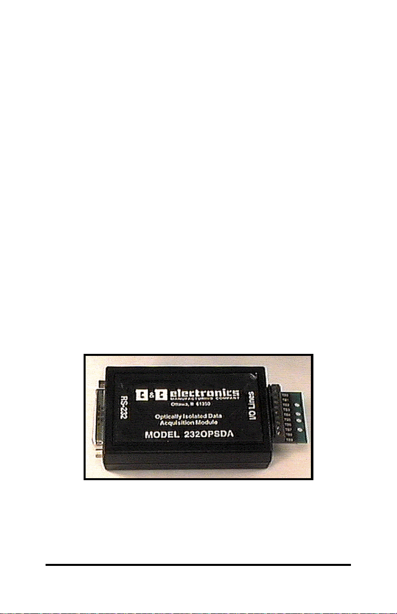
The 232OPSDA is an optically isolated data acquisition module
that is connected to your computer’s RS-232 ser ial port. It provides
2500V of optical isolation protection between the I/O and RS-232
side of the module. The 232OPSDA offers six channels of 12-bit
A/D, one digital input, and one digital output. The six A/D input
channels can be used for a number of applications. One A/D
channel can read a 4-20mA analog cur rent, two buffered channels
read voltages between 0 and 5V, two non-buffered channels read
voltages between 0 and 5V, and one channel can read voltages
between 0 and 10V.
The 232OPSDA connects to your computer’s RS-232 serial port
through a DB-25S (female) connector. The module automatically
detects baud rates from 1,200 to 9,600. A data for m at of 8 data bits,
1 stop bit, and no parity is used.
The RS-232 side of the 232OPSDA is port powered. Power is
drawn from RT S and DTR regardless of whether they are asserted
HIGH or LOW. In addition, an isolated external power supply is
required to power the I/O side of the module. Both port-powering
and the external power supply are required. The 232OPSDA
requires a power supply that produces 9-16VDC @ 10mA (not
including power consumption of external devices).
Figure 1.1: 232OPSDA Module
Documentation Number 232OPSDA1397 Manual 1
B&B Electronics -- PO Box 1040 -- Ottawa, IL 61350
PH (815) 433-5100 -- FAX (815) 433-5105
Page 5
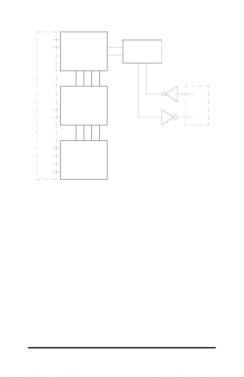
Terminal Blocks
Digital Input
TB 7
Digital Output
TB 6
O
/
I
l
a
t
i
g
i
D
TB 4
TB 5
g
o
l
a
n
A
TB 0
TB 1
TB 2
TB 3
Microprocessor
A/D Converter
A/D 4
A/D 5
s
t
u
p
n
I
A/D 0
A/D 1
A/D 2
A/D 3
Packing List
Optical Isolation
0
1
2
D
/
A
0
D
/
A
3
D
D
D
/
/
/
A
A
A
2
1
3
D
D
D
/
/
/
A
A
A
Signal
Conditioning
Circuitry
Figure 1.2: General Block Diagram
Serial Port
DB-25S
TD
RD
RS-232
Tranceiver
Examine the shipping carton and the contents for physical
damage. The following items should be in the shipping carton:
1. 232OPSDA module
2. One 232OPSDA 3.5” disk
3. This instruction manual
If any of these items are missing or damaged, contact B&B
Electronics immediately.
2 Documentation Number 232OPS DA1397 Manual
B&B Electronics -- PO Box 1040 -- Ottawa, IL 61350
PH (815) 433-5100 -- FAX (815) 433-5105
Page 6

Software Installation
The 232OPSDA comes with several a demonstration program.
To install these programs on your hard drive:
1. Place the disk in drive A.
2. Type A: and press the <ENTER> key.
3. Type INSTALL and press the <ENTER> key.
4. Follow the instructions given by the program.
The file, READ.ME, contains corr ections and additions to the printed
user’s manual. The file, FILES.LST, contains a list and description of
the files installed on the hard drive. The file, HISTORY.LST,
contains a historic description of the 232OPSDA.
232OPSDA Specifications
Analog to Digital Converter
Resolution: 12 bit
Channels: 6
A/D Connections: Terminal Blocks
4-20mA channel: 1
Input Resistance: 10Ω
Input Offset voltage: 1500µV
Input Offset Voltage Drift: 0.5µV/°C
Signal Conditioning Error: ±3% of output
0 to 5V Buffered Input Channels: 2
Input Resistance: 1TΩ
Input Offset voltage: 1500µV
Input Offset Voltage Drift: 0.5µV/°C
Signal Conditioning Error: ±1% of output
0 to 10V Input Channel: 1
Input Resistance: 200KΩ
Input Offset voltage: 1500µV
Input Offset Voltage Drift: 0.5µV/°C
Signal Conditioning Error: ±1% of output
0 to 5V Non-buffered Input Channels: 2
Input Offset voltage: 1500µV
Input Offset Voltage Drift: 0.5µV/°C
Total Unadjusted Error: ±1.75LSB
Non-buffered A/D input channels must be driven from a
source impedance less than 1KΩ.
Documentation Number 232OPSDA1397 Manual 3
B&B Electronics -- PO Box 1040 -- Ottawa, IL 61350
PH (815) 433-5100 -- FAX (815) 433-5105
Page 7

Digital Input
Channels: 1
Voltage Range: -30VDC to +30VDC
Low Voltage: -30VDC to 1.0VDC
High Voltage: 2.0VDC to 30VDC
Leakage Current: 1 µA maximum
Digital Output
Channels: 1
Low Voltage: 0.6VDC @ 8.7mA
High Voltage: 4.3VDC @ -5.4mA
Power Supply
Input Voltage: 9-16VDC @ 10mA (Does not include the
power consumption of external devices.)
Connections: Terminal Blocks
Communications
Standard: RS-232 (unit is DCE)
Baud Rate: 1,200 to 9,600 (automatic detection)
Format: 8 data bits, 1 stop bit, no parity
Isolation Protection: 2500V (Power supply not considered)
Port Power: RTS and DTR (either state)
Connections: DB-25S (female)
4 Documentation Number 232OPS DA1397 Manual
B&B Electronics -- PO Box 1040 -- Ottawa, IL 61350
PH (815) 433-5100 -- FAX (815) 433-5105
Page 8
Chapter 2: Connections
This chapter will cover the connections required for the
232OPSDA. Four sets of connections are required: A/D converter,
digital I/O, serial port, and power supply connections. Do not make
any connections until you have read this chapter. If you do not use a
particular type of connection, it is still im portant to r ead eac h section.
Table 2.1 shows the terminal block assignments.
Terminal
Block
TB 0 A/D 0
TB 1 A/D 1
TB 2 A/D 2 Buffered 0 to 5V A/D Channel
TB 3 A/D 3 0 to 10V A/D Channel
TB 4 A/D 4 Non-buffered 0 to 5V A/D Channel
TB 5 A/D 5 Non-buffered 0 to 5V A/D Channel
TB 6 Digital out Digital Output
TB 7 Digital in Digital Input
GND GND Ground
+12VDC +12VDC Power Supply Connection
* The current loop input uses a non-inverting amplifier that has a
gain of 23.064. Space for through-hole resistors is provided to
change the gain. By decreasing the gain, currents up to 100mA can
be read with A/D 0.
** This A/D input uses a voltage follower cir cuit. Spaces for throughhole resistors are provided to convert the voltage fo llower into a noninverting amplifier with gain > 1.
Table 2.1: Terminal Block Assignments
Function Description
4-20mA Current Loop Input Channel*
Buffered 0 to 5V A/D Channel**
A/D Connections
The A/D connections are m ade on the I/O port which consists of
ten terminal blocks. Terminal Blocks 0-5 are A/D channels 0-5.
These six A/D channels are ref erenced to GND (terminal block 8).
The 4-20mA Current Loop A/D channel requires connections
different from the other five c hannels, so two different diagram s are
shown for required A/D connections. Figure 2.1 shows the
connections required f or the 4-20mA Current Loop c hannel (A/D 0),
and Figure 2.2 shows the connec tions required for A/D channels 1-
5.
Documentation Number 232OPSDA1397 Manual 5
B&B Electronics -- PO Box 1040 -- Ottawa, IL 61350
PH (815) 433-5100 -- FAX (815) 433-5105
Page 9
RS-232 Port
232OPSDA
1
0
D
D
/
/
A
A
2
1
0
B
B
B
T
T
T
2
3
5
4
D
D
/
/
A
A
3
4
B
B
T
T
D
D
D
N
/
/
G
A
A
5
8
B
B
T
T
Output
4-20mA
Current Loop
Transmitter
Return
4-20mA Current
Loop
Input
4-20mA
Current Loop
Receiver
Out
Figure 2.1: Current Loop Channel Connections (A/D 0)
NOTE: W hen using the 4-20mA Current Loop Input with the setup
shown in Figure 2.1, A/D 1-5 cannot be used and should be
connected to the terminal block labeled GND.
A
D
S
P
O
2
3
2
A/D 1
TB 1
TB 2
A/D 2
TB 3
A/D 3
TB 4
A/D 4
TB 5
A/D 5
TB 0
A/D 0
TB 8
GND
0 to 5VDC Input
0 to 5VDC Input
0 to 10VDC Input
0 to 5VDC Input
0 to 5VDC Input
GND
Figure 2.2: Required Connections for A/D 1- A/D 5
6 Documentation Number 232OPS DA1397 Manual
B&B Electronics -- PO Box 1040 -- Ottawa, IL 61350
PH (815) 433-5100 -- FAX (815) 433-5105
Page 10

Digital I/O Connections
t
The digital I/O connections are made on the I/O port, which
consists of terminal blocks. Table 2.1 shows the terminal block
assignments.
Digital Input
T erminal bloc k 7 is the digital input line. T his input is CMOS/TTL
compatible and can handle voltage from -30VDC to 30VDC. If a
digital input is from -30VDC to 1.0VDC, the state will be read as a
“0” (LOW ). If a digital input is from 2.0VDC to 30VDC, the state will
be read as a “1” (HIGH). If the digital input is not used, it should be
connected to GND. Figure 2.3 show the connec tions r equired for the
digital input.
Digital Output
T erm inal Block 6 is the digital output line. This line is CMOS/T TL
compatible. W hen the digital output is set to “0” (LOW ), the output
voltage will be between 0 and 0.6VDC. When the digital output is set
to “1” (HIGH), the output voltage will be between 4.3VDC to 5.0VDC.
Figure 2.3 shows the connections required for the digital output.
GND
TB 6
TB 7
TB 8
Digital Output
A
D
S
P
Digital Input
O
2
3
2
Figure 2.3: Digital I/O Required Connections
0 to 5VDC Output
-30VDC to 30VDC Inpu
To Device GND
Serial Port Connections
In order to com municate with the 232OPSDA m odule it must be
connected to an RS-232 serial port. The unit autom atically detects
baud rates from 1,200 to 9,600. A data f ormat of 8 data bits, 1 stop
bit and no parity is used. The 232OPSDA is c onfigured as a DCE
device (See Table 2.2). If your communications equipment is
configured as a DTE device, s uch as a standar d IBM PC serial port,
the 232OPSDA should be connected using a “str aight through” DB25 cable or a standard DB-9 to DB-25 cable adapter as shown in
Table 2.3. If your communications equipment is configured as a
DCE device, such as a modem, the 232OPSDA should be
connected using a “null modem” cable (See Table 2.4).
Documentation Number 232OPSDA1397 Manual 7
B&B Electronics -- PO Box 1040 -- Ottawa, IL 61350
PH (815) 433-5100 -- FAX (815) 433-5105
Page 11

Table 2.2 - RS-232 Connector Pinout
DB25S
Pin #
Signal
232OPSD
A Function
Notes
2 Transmit Data (TD) Input Connection is required.
3 Receive Data (RD) Output Connection is required.
4 Request to Send (RTS) Input Used for power.
5 Clear to Send (CTS) Internally connected to
RTS (pin 4).
6 Data Set Ready (DSR) Internally connected to
DTR (pin 20).
7 Signal Ground (SG) Connection is required.
8 Data Carrier Detect (DCD) Internally connected to
to DTR (pin 20).
12 Signal Ground (SG)
20 Data Terminal Ready
Input Used for power.
(DTR)
25 Optional Power Supply
Connection
Connect Power Supply
to this pin if RTS and
DTR are not available
Table 2.3 - 232OPSDA To DTE Connections
232SPDA
Pin #
Signal
DTE DB-25
Connection
DTE DB-9
Connection
2 Transmit Data (TD) 2 3
3 Receive Data (RD) 3 2
4 Request to Send (RTS) 4 7
5 Clear to Send (CTS) 5 8
6 Data Set Ready (DSR) 6 6
7 Signal Ground (SG) 7 5
8 Data Carrier Detect (DCD) 8 1
20 Data Terminal Ready (DTR) 20 4
Table 2.4 - 232OPSDA To DCE Connections
232OPSDA
Pin #
Signal
DCE DB-25
Connection
DCE DB-9
Connection
2 Transmit Data (TD) 3 2
3 Receive Data (RD) 2 3
4 Request to Send (RTS) 5 8
5 Clear to Send (CTS) 4 7
6 Data Set Ready (DSR) 20 4
7 Signal Ground (SG) 7 5
8 Data Carrier Detect (DCD) N/C N/C
20 Data Terminal Ready (DTR) 6 6
8 Documentation Number 232OPS DA1397 Manual
B&B Electronics -- PO Box 1040 -- Ottawa, IL 61350
PH (815) 433-5100 -- FAX (815) 433-5105
Page 12

Power Supply Connections
The 232OPSDA requires an isolated external power supply that
is able to produce 9-16VDC @10mA in addition to the port power.
The positive(+) lead of the power supply is connected to the terminal
block labeled +12VDC and the negative(-) lead is connected to the
terminal block labeled GND. The external power supply powers the
I/O side of the module. The RS-232 side of the module is port
powered using RTS and DTR. These lines may be either LOW or
HIGH to provide power to the module. The two sources of power are
required for optical isolation.
Documentation Number 232OPSDA1397 Manual 9
B&B Electronics -- PO Box 1040 -- Ottawa, IL 61350
PH (815) 433-5100 -- FAX (815) 433-5105
Page 13

Chapter 3: Commands
Only three commands are required to operate the 232OPSDA:
the read A/D command, read digital I/O command, and the set
digital output comm and. The com m and string cons ists of f our bytes.
The read A/D and digital I/O commands require an additional data
byte. See Table 3.1.
Function Command Response
Read A/D
Channels
Read
Digital I/O
Set Digital
Output
NOTE: Each {…} represents one byte.
In addition to the com m ands mentioned above, an ex tended set
of commands are provided that support bit-error identification.
These comm ands use the “ #” character in place of the “!” character ,
and the compliment of the data byte must be sent after the data
byte. The extended commands are shown in table 3.2.
Function Command Response
Read A/D
Channels
Read
Digital I/O
Set Digital
Output
NOTE: ~{…} represents the complement of one byte.
Before going into the specifics of each comm and, it is important
to understand that a byte has a value from 0 to 255 and can be
represented in decimal (0 to 255) , hexadecimal (00 to FF) , or by an
ASCII character. The c ommands in Table 3.1 are shown in ASCII,
for example: “!0RD”. The decimal and hexadecimal equivalents of
some ASCII characters are shown in Table 3.2. Notice that the
ASCII representation of the character “ 0” does not have a value of 0.
Refer to Appendix A for more ASCII, decimal, and hexadecimal
equivalents.
Table 3.1: 232OPSDA Commands
!0RA{#} {ch#msb}{ch#lsb}{ch(#-1)msb}…
{ch0msb}{ch0lsb}
!0RD {I/O states}
!0SO{#} no response
Table 3.1: 232OPSDA Commands
#0RA{#}~{#} {ch#msb}~{ch#msb}{ch#lsb}{ch#lsb}
{ch(#-1)msb}~{ch(#-1)msb}….{ch0msb}
~{ch0msb}{ch0lsb}~{ch0lsb}
#0RD {I/O states}~{I/O states}
#0SO{#}~{#} no response
Documentation Number 232OPSDA1397 Manual 11
B&B Electronics -- PO Box 1040 -- Ottawa, IL 61350
PH (815) 433-5100 -- FAX (815) 433-5105
Page 14

Table 3.2 - Equivalent Values
ASCII Decimal Hexadecimal
! 33 21h
# 35 23h
0 48 30h
A 65 41h
D 68 44h
O 79 4Fh
R 82 52h
S 83 53h
NUL 0 0h
SOH 1 1h
STX 2 2h
ETX 3 3h
EOT 4 4h
ENQ 5 5h
ACK 6 6h
BEL 7 7h
Syntax
As mentioned earlier, the com m and string consists of four bytes.
The first byte is the start of message byte. The start of message
byte is always the “!” character. The second byte is the address byte.
This byte allows each unit to have a unique address (useful in RS485 networks). Since the 232OPSDA uses RS-232 com munications,
this byte is the ASCII “0” (zero) character and cannot be changed.
The next two bytes are the comm and characters. These bytes are
used to specify which command will be executed by the module.
Some commands require a fifth byte, a data byte.
Command Syntax: !0___
|||||
||||Data Byte
|||2
||1
| Address Byte
Start of Message Byte
nd
command Byte
st
Command Byte
12 Documentation Number 232OPS DA1397 Manual
B&B Electronics -- PO Box 1040 -- Ottawa, IL 61350
PH (815) 433-5100 -- FAX (815) 433-5105
Page 15

The comm and syntax for the extended command set is shown
below:
Command Syntax: #0____
||||||
|||||Compliment
||||Data Byte
|||2
||1
nd
Command Byte
st
Command Byte
| Address Byte
Start of Message Byte
Reading A/D Channels Command
The Read A/D channels command returns two bytes for each
channel read. The two bytes represent the most significant byte
(MSB) and least significant byte (LSB) of the reading. The MSB is
received first, f ollowed by the LSB. This command requires a data
byte. The data byte is used to specify the number of the highest
channel to be read. All channels less than this c hannel will be read
as well. For example, if the data byte has a value of 3, then channels
0 to 3 will be read. The highest channel is read first.
Command Syntax
!0RA{#}
Where “{#}” is a byte that specifies the number of the highest
channel to be read. See Table 3.3
Response Syntax
{ch(#)MSB}{ch(#)LSB}{ch(#-
1)MSB}...{ch0MSB}{ch0LSB}
The most significant byte of the channel specified is received
first. The least signif icant byte and the lower channels will follow in
descending order. “{chxMSB}” and “{chxLSB}” represent the most
and least significant bytes of the A/D conversion result.
Documentation Number 232OPSDA1397 Manual 13
B&B Electronics -- PO Box 1040 -- Ottawa, IL 61350
PH (815) 433-5100 -- FAX (815) 433-5105
Page 16

Table 3.3 - Read A/D Response
# of Channels Specified Response
decimal Hex ASCII
Channels Returned
(order of response)
Bytes
Returned
0 0 NUL Channel 0 2
1 1 SOH Channels 1,0 4
2 2 STX Channels 2,1,0 6
3 3 ETX Channels 3,2,..,0 8
4 4 EOT Channels 4,3,..,0 10
5 5 ENQ Channels 5,4,..,0 12
NOTE: There are three test c hannels that can be r ead: Ref+, Ref-,
and Ref+/2. Specify 13 (0Dh) to read Ref +, 12 (0Ch) to read Ref-,
and 11 (0Bh) to read Ref+/2.
Reading Digital I/O Command
T he Read Digital I/O command returns a byte which represents
the state of the digital input and digital output. Bit 0 corresponds to
the state of the digital output, and bit 3 corresponds to the state of
the digital input. If a bit is a 0 then the digital state of that digital I/O is
LOW. If a bit is a 1 then the digital state of the I/O is HIGH. NOTE:
Bits 1-2 and 4-7 of the data byte are ignored.
Command Syntax
!0RD
Unit Response
{states}
Where {states} is a byte in which bits 0 corresponds to the current
state of the digital output and bit 3 corresponds to the curr ent state
of the digital input.
Set Digital Output Command
T he Set Digital Output command is us ed to set the state of the
digital output line. This command requires a data byte. The data byte
is used to spec ify the output state. Bits 0 corr esponds to the s tate of
the digital output. If bit 0 is a 0 then the output will be set LOW. If bit
0 is a 1 then the output will be set HIGH. NOTE: This command
ignores bits 1-7 of the data byte.
Command Syntax
!0SO{states}
Where {states} is a byte in which bit 0 corresponds to the output
state of the digital outputs.
Unit Response
no response
14 Documentation Number 232OPS DA1397 Manual
B&B Electronics -- PO Box 1040 -- Ottawa, IL 61350
PH (815) 433-5100 -- FAX (815) 433-5105
Page 17

Chapter 4: A/D
This chapter will deal with the various A/D channels and
manipulating the data obtained from them.
Sampling Rate
The A/D converter has a conversion time around 10
microseconds, however, the actual sampling rate is limited by the
serial communications. The actual sampling rate for a single
channel is around 120 samples per second (9600 baud). This rate
drops to around 41 samples per second when sampling all of the
channels. When reading an A/D input, the 232OPSDA takes four
readings and returns the average (0.5 and greater are rounded up)
of these readings. This averaging helps filter out noise.
A/D Converter Range
The actual A/D converter chip in the 232OPSDA is a 12 bit A/D
converter that can read analog voltages between 0 and 5VDC.
However, the 232OPSDA contains signal conditioning c ircuitry that
allows you to measure voltages from 0 to 10VDC (Gain = 0.5) as
well as other ranges. In the following sections, each channel
configuration will be covered.
Non-buffered 0 to 5VDC A/D Inputs
The 232OPSDA has two non-buffered 0 to 5V inputs. They are
A/D 4 on Terminal Block 4 and A/D 5 on Terminal Block 5. The
voltage applied to the Terminal Block s is the voltage that is read by
the A/D converter chip. The driving source impedance should be
less than 1KΩ for these two channels.
Buffered 0 to 5V A/D Inputs
The 232OPSDA has two buf fered 0 to 5V inputs. T hey are A/D 1
on Terminal Block 1 and A/D 2 on Terminal Block 2. An operational
amplifier is s etup as a voltage follower to buffer the A/D converter
from the source of the voltage. The input resistance of eac h of these
channels is 1TΩ. This allows you to have a large source impedance.
Both A/D 1 and A/D 2 are set up as voltage followers with a gain
of 1 when they leave the factor y. However, the voltage follower for
A/D 1 (TB 1) has spaces for optional through hole resistors. This
allows you to reconfigure A/D 1 into a non-inverting amplifier
configuration. A non-inverting am plifier c an have a gain greater than
1. See the circuit schematic in Figure B.1 and board layout in Figure
B.2 in Appendix B. To change the voltage follower into a non-
Documentation Number 232OPSDA1397 Manual 15
B&B Electronics -- PO Box 1040 -- Ottawa, IL 61350
PH (815) 433-5100 -- FAX (815) 433-5105
Page 18

inverting amplifier, remove R15 and calculate values for R13 and
R
R14 using the equation below.
V
Gain
0
==+
Vin
NOTE: V
the voltage at TB1. R13 and R14 should be chosen so that V
not exceed 5.00VDC.
0 to 10VDC A/D Input
The 232OPSDA contains one A/D input than is capable of
handling voltages between 0VDC and 10VDC. This channel is A/D 3
and is located on Terminal Block 3. The gain of the signal
conditioning circuitry for this channel is 0.5. If 10VDC is applied to
Terminal Bloc k 3, the A/D Converter chip will read 5.00V. The input
resistance of this channel is 200KΩ, so the driving source
impedance should be less than 1KΩ to minimize voltage division
error.
4-20mA Current Loop A/D Input
The 232OPSDA has one A/D c hannel capable of monitoring the
loop current in a 4-20mA analog current loop. See figure B.1 in
Appendix B for a circuit schematic. A 10Ω resistor is connected
between TB 0 and GND inside the 232OPSDA. The voltage drop
across this resistor is proportional to the current in the current loop.
With the original c onf igur ation, the f ollowing equation can be used to
convert the voltage read by the A/D converter chip to the actual
current in the loop. The value 23.064 is the gain of the signal
conditioning circuitry
NOTE: AD
voltage is between 0 and 5.00VDC.
is the voltage read by the A/D converter chip, and Vin is
0
LoopCurrent mAAD=
is the voltage read by the A/D converter chip. This
0
()
R13
1
14
×
1000
23064 10
×
. Ω
does
0
0
16 Documentation Number 232OPS DA1397 Manual
B&B Electronics -- PO Box 1040 -- Ottawa, IL 61350
PH (815) 433-5100 -- FAX (815) 433-5105
Page 19

The signal conditioning circuit for this A/D input channel has been
designed to be easily modif ied. In the original configuration, R5 and
R6 are left OPEN (they are not present). These two spaces are
provided if you need a different gain. Reducing the gain of this noninverting amplifier allows you to measure c urrents up to 100m A, and
increasing the gain allows you to read much smaller currents with
greater accuracy. See the circuit schem atic in Figure B.1 and board
layout in Figure B.2 in Appendix B.
To change the gain of this non-inverting amplifier, remove R8
and R9, and calculate values for R4 and R5 using the equation
below.
V
Gain
=
×
10
NOTE: V
current) is the voltage drop across the 10Ω resistor. R4 and R5
should be chosen so that V
NOTE: Decreasing the gain allows you to measure larger cur rents,
but the maximum current that can be read is 100mA. The 100mA
limit is due to the power rating of the 10Ω resistor (0.125W).
NOTE: When using the 4-20mA current loop input, A/D 1 - A/D 5
should be connected to the terminal block labeled GND.
is the voltage read by the A/D converter and (10 x loop
0
0
LoopCurrent
does not exceed 5.00VDC.
0
=+
1
R
5
R
4
Documentation Number 232OPSDA1397 Manual 17
B&B Electronics -- PO Box 1040 -- Ottawa, IL 61350
PH (815) 433-5100 -- FAX (815) 433-5105
Page 20

Chapter 5: Software
g
Application Program Interface
The application program interface (API) is a set of routines that
makes it easy to comm unicate with the 232OPSDA module f rom a 16bit DOS application. Example programs using the API are written in
Borland C++, Borland Pascal and Microsoft
batch file, MAKEIT.BAT, in the dir ectory for each language shows how
to compile and link the demo program with the API routines.
B232OPSDA_ReadAnalog
®
QuickBASIC v4.5. The
Purpose:
This function reads the A/D input channels.
Syntax:
Remarks:
C:
Pascal:
BASIC:
hComDev is the handle to a serial port where the
BOOL B232OPSDA_ReadAnalog (WORD hComDev,
BYTE modAddr, WORD channels, WORD* data);
function B232OPSDA_ReadAnalog (hComDev :
word; modAddr : byte; channels : word;
data : Pword);
FUNCTION B232OPSDAReadAnalog (BYVAL
hComDev AS INTEGER, BYVAL modAddr AS
INTEGER, BYVAL channels AS INTEGER, BYVAL
wdataseg AS INTEGER, BYVAL wdataoff AS
INTEGER)
module is connected. This is the value returned by
initComPort. modAddr is the module address, which
is always 30H (48 decimal) for the 232OPSDA m odule.
channels is a bit mask for the A/D input channels that
should be read. See the table below for the meaning of
each bit.
Bit Channel Value
(hex)
Bit 7 (nothing) 80H 128
Bit 6 (nothing) 40H 64
Bit 5 A/D Channel 5 20H 32
Bit 4 A/D Channel 4 10H 16
Bit 3 A/D Channel 3 08H 8
Bit 2 A/D Channel 2 04H 4
Bit 1 A/D Channel 1 02H 2
Bit 0 A/D Channel 0 01H 1
data is that address of an array of 16-bit values where
Value
(decimal)
the results of the A/D conversion will be stored.
For QuickBASIC users: wdatase
Documentation Number 232OPSDA1397 Manual 19
B&B Electronics -- PO Box 1040 -- Ottawa, IL 61350
PH (815) 433-5100 -- FAX (815) 433-5105
and wdataoff are the
Page 21

segment and offset addresses of the integer array where
the results of the A/D conversion will be stored.
Returns:
FALSE (zero) if the function fails, otherwise it returns
TRUE (non-zero).
B232OPSDA_ReadDigital
Purpose:
Syntax:
Remarks:
Returns:
This function reads the states of all the digital I/O lines.
C:
Pascal:
BOOL B232OPSDA_ReadDigital (WORD hComDev,
BYTE modAddr, WORD* data);
function B232OPSDA_ReadDigital (hComDev :
word; modAddr : byte; data : Pword);
BASIC:
FUNCTION B232OPSDAReadDigital (BYVAL
hComDev AS INTEGER, BYVAL modAddr AS
INTEGER, BYVAL wdataseg AS INTEGER, BYVAL
wdataoff AS INTEGER)
hComDev is the handle to a serial port where the
module is connected. This is the value returned by
initComPort. modAddr is the m odule address. This is
always 30H (48 decimal) for the 232OSPSDA module.
data is the address of the 16-bit value where the digital
I/O values will be stored. If bit 0 (01H; 1 decim al) of data
is set, then digital input 0 is on, otherwise it is off. If bit 4
(10H; 16 decimal) of data is set, then digital output 1 is
on, otherwise it is off.
For QuickBASIC users: wdataseg and wdataoff are the
segment and of fset addresses of the integer the digital
I/O values will be stored.
FALSE (zero) if the function fails, otherwise it returns
TRUE (non-zero).
20 Documentation Number 232OPS DA1397 Manual
B&B Electronics -- PO Box 1040 -- Ottawa, IL 61350
PH (815) 433-5100 -- FAX (815) 433-5105
Page 22

B232OPSDA_SetDigitalOutput
Purpose:
This function sets the states of the digital output lines.
Syntax:
Remarks:
C:
Pascal:
BASIC:
hComDev is the handle to a serial port where the
module is connected. This is the value returned by
initComPort. modAddr is the module address. This
is always 30H (48 decimal) for 232OPSDA module.
lines is a bit mask of the digital outputs to c hange. This
will always be 01H (1 decimal) of the 232OPSDA,
because it only has one digital output line. states is the
new state of the digital outputs specif ied in lines. This
can be either zero for OFF or non-zero for ON.
Returns:
FALSE (zero) if the function fails, otherwise it returns
TRUE (non-zero).
deinitComPort
BOOL B232OPSDA_SetDigitalOutput (WORD
hComDev, BYTE modAddr, WORD lines, WORD
states);
function B232OPSDA_ReadDigitalOutput
(hComDev : word; modAddr : byte; lines :
word; states : word);
FUNCTION B232OPSDAReadDigitalOutput
(BYVAL hComDev AS INTEGER, BYVAL modAddr
AS INTEGER, BYVAL lines AS INTEGER, BYVAL
states AS INTEGER)
Purpose:
Syntax:
Remarks:
Removes the serial communications port driver.
C:
Pascal:
BASIC:
void deinitComPort (WORD hComDev);
procedure deinitComPort (hComDev : word);
sub deinitComPort (BYVAL hComDev AS
INTEGER);
This function must be called after a serial
communic ations port is installed with initComPort to
remove the interrupt service routine that it installs.
Returns:
See Also:
Nothing.
initComPort
initComPort
Purpose:
Documentation Number 232OPSDA1397 Manual 21
Installs a serial communications port driver.
B&B Electronics -- PO Box 1040 -- Ottawa, IL 61350
PH (815) 433-5100 -- FAX (815) 433-5105
Page 23

Syntax:
C:
WORD initComPort (WORD portAddr, BYTE irq,
LONG baudRate);
Pascal:
function initComPort (portAddr : word; irq
: byte; baudRate : longint) as integer;
BASIC:
FUNCTION initComPort% (BYVAL portAddr AS
INTEGER, BYVAL irq AS INTEGER, BYVAL
baudRate AS INTEGER)
Remarks:
portAddr is the address of the serial port. irq is the
interrupt request number that the serial port uses.
baudRate is the speed at which the API talkes to the
232OPSDA module. Common port addresses and irq
numbers are are:
Port Address IRQ
COM1 3F8H 4
COM2 2F8H 3
COM3 3E8H 4
COM4 2E8H 3
deinitComPort must be called to rem ove the inter rupt
service routine installed by initComPort. The results
are unpredictable if you terminate your application
without calling deinitComPort.
Returns:
A handle that uniquely identifies the installed serial port.
See Also:
deinitComPort
Low-Level Communications
This section covers the low-level commands that are sent to the
module through a serial communications port and the responses
from the module. Detailed discussion of the command and
responses are covered in Chapter 3. The examples shown here are
in Microsoft® QuickBASIC. If you are programming in another
language, this information can be used as a guideline for
programming for the 232OPSDA module. To open and close a serial
communications port in QuickBASIC use:
22 Documentation Number 232OPS DA1397 Manual
B&B Electronics -- PO Box 1040 -- Ottawa, IL 61350
PH (815) 433-5100 -- FAX (815) 433-5105
Page 24

‘ Open the serial port.
‘
OPEN “COM1:9600,N,8,1,cd,ds” FOR RANDOM AS #1
PAUSE (.5)
‘ Close the serial port when finished.
‘
CLOSE #1
Read A/D Command
The read A/D c hannels command returns two bytes of data for
each channel read. The two bytes represent the most significant
byte (MSB) and least significant byte (LSB) of the reading. The MSB
is received first, followed by the LSB. This co m m and requires a data
byte. The data byte is used to specify the number of the highest
channel to be read. All channels less than this c hannel will be read
as well.
Step 1 - Constructing the command string:
Command$ = “!0RA” + CHR$(channel)
The value of channel is equal to the highest channel to be read.
Step 2 - Transmitting the command string:
Print #1, Command$;
Step 3 - Receiving the data:
MSB$ = INPUT$(1, #1)
LSB$ = INPUT$(1, #1)
Step 4 - Manipulating the data:
reading = (ASC(MSB$) * 256) + ASC(LSB$)
The value of reading is the result of the A/D conversion.
Documentation Number 232OPSDA1397 Manual 23
B&B Electronics -- PO Box 1040 -- Ottawa, IL 61350
PH (815) 433-5100 -- FAX (815) 433-5105
Page 25

Step 5 - Repeat Step 3 and 4 until each channel has been
completed.
Step 6 - The various A/D channels have signal conditioning, so
mathematical manipulation of the voltage read will have to be
performed. See Chapter 4 for the equations.
Example 5.1 - Read A/D channels 1 and 0
gain0 = 23.064
gain1 = 1!
channel = 1
Command$ = “!0RA” + CHR$(channel)
Print #1, Command$;
‘ Get the value of channel 1
MSB$ = INPUT$ (1, #1)
LSB$ = INPUT (1, #1)
ad1 = (ASC(MSB$) * 256) + ACS(LSB$)
reading1 = 5! * ad1 / (gain1 * 4095!)
‘ Get the value of channel 0
MSB$ = INPUT$ (1, #1)
LSB$ = INPUT$ (1, #1)
ad0 = (ASC(MSB$) * 256) + ACS(LSB$)
reading0 = (((ad0 * 1000!) / 4095!) * 5!) / (10!
*
gain0)
The value of reading1 is the result of the A/D convers ion on channel
1. The value of reading0 is the result of the A/D conversion on
channel 0.
Read Digital I/O Command
T he Read Digital I/O command returns a byte which represents
the states of the digital input and digital output. Bit 0 corres ponds to
the state of digital output. Bit 3 corresponds to the state of digital
input. If a bit is a 0 then the digital state of that digital I/O is LOW. If
a bit is a 1 then the digital state of the I/O is HIGH.
24 Documentation Number 232OPS DA1397 Manual
B&B Electronics -- PO Box 1040 -- Ottawa, IL 61350
PH (815) 433-5100 -- FAX (815) 433-5105
Page 26

Step 1 - Constructing the command string:
Command$ = “!0RD”
Step 2 - Transmitting the command string:
Print #1, Command$
Step 3 - Receiving the data:
Reply$ = INPUT$ (1, #1)
Step 4 - Manipulating the data:
states = ASC(Reply$)
Step 5 - Determining an I/O’s status
status = states AND mask
By “ANDing” the value of states with the appropriate mask of an I/O
line, the status of can be determined. If status is equal to zero then
the I/O line is LOW . If status is not equal to zero then the I/O line is
HIGH. Table 5.1 shows the mask values for each I/O.
Table 5.1 - Digital I/O Mask Val u es
Mask Values
I/O Line Hexadecimal Decimal
Digital Output #0 1H 1
Digital Input #0 8H 8
Step 6 - Repeat Step 5 until the status of each I/O has been
determined.
Example 5.2 - Determining the status of Digital Input #0 of the
module.
mask = &H8
Command$ = “!0RD”
Print #1, Command$
Reply$ = INPUT$ (1, #1)
states = ASC (Reply$)
status = states AND mask
If status is equal to zero than Digital Input #0 is LOW. If status is not
equal to zero than Digital Input #0 is HIGH.
Documentation Number 232OPSDA1397 Manual 25
B&B Electronics -- PO Box 1040 -- Ottawa, IL 61350
PH (815) 433-5100 -- FAX (815) 433-5105
Page 27

Set Digital Output State
T he Set Digital Output command is us ed to set the state of the
digital output line. This command requires a data byte. The data byte
is used to specify the output state. Bit 0 corresponds to the state of
digital output. If a bit is a 0 then the output will be set LOW. If a bit is
a 1 then the output will be set HIGH. Note: This command ignores
Bits 1-7 of the data byte.
Step 1a - Constructing the command string:
‘ Set Output HIGH
states = states OR mask
By “ORing” the current states with the appropriate mask of the digital
output (given in Table 5.1), the output’s data bit will be set to a “1”
(which will be set HIGH).
Step 1b - Set Output LOW
states = states AND (NOT(mask))
By “ANDing” the current states with the complement of the
appropriate mask of a digital output (given in T able 5.1), the output’s
data bit will be set to a “0” (which will be set LOW).
Step 1c - Construct the string
Command$ = “!0SO” + CHR$(states)
Step 2 - Transmitting the command string:
Print #1, Command$
Example 5.3 - Set Digital Output #0 HIGH.
‘ Set bit 0 to make Digital Output #0 HIGH
states = states OR 1
Command$ = “!0SO” + CHR$(states)
Print #1, Command$
Digital Output #0 will be set HIGH. Note that the variable states is
assumed to be the value from Example 5.2.
26 Documentation Number 232OPS DA1397 Manual
B&B Electronics -- PO Box 1040 -- Ottawa, IL 61350
PH (815) 433-5100 -- FAX (815) 433-5105
Page 28

Appendix A: Decimal to Hex to ASCII Conversion
DECIMAL to HEX to ASCII CONVERSION TABLE
DEC HEX ASCII KEY DEC HEX ASCII DEC HEX ASCII DEC HEX ASCII
0 0 NUL ctrl @ 32 20 SP 64 40 @ 96 60 `
1 1 SOH ctrl A 33 21 ! 65 41 A 97 61 a
2 2 STX ctrl B 34 22
3 3 ETX ctrl C 35 23 # 67 43 C 99 63 c
4 4 EOT ctrl D 36 24 $ 68 44 D 100 64 d
5 5 ENQ ctrl E 37 25 % 69 45 E 101 65 e
6 6 ACK ctrl F 38 26 & 70 46 F 102 66 f
7 7 BEL ctrl G 39 27 ' 71 47 G 103 67 g
8 8 BS ctrl H 40 28 ( 72 48 H 104 68 h
9 9 HT ctrl I 41 29 ) 73 49 I 105 69 i
10 A LF ctrl J 42 2A * 74 4A J 106 6A j
11 B VT ctrl K 43 2B + 75 4B K 107 6B k
12 C FF ctrl L 44 2C , 76 4C L 108 6C l
13 D CR ctrl M 45 2D - 77 4D M 109 6D m
14 E SO ctrl N 46 2E . 78 4E N 110 6E n
15 F SI ctrl O 47 2F / 79 4F O 111 6F o
16 10 DLE ctrl P 48 30 0 80 50 P 112 70 p
17 11 DC1 ctrl Q 49 31 1 81 51 Q 113 71 q
18 12 DC2 ctrl R 50 32 2 82 52 R 114 72 r
19 13 DC3 ctrl S 51 33 3 83 53 S 115 73 s
20 14 DC4 ctrl T 52 34 4 84 54 T 116 74 t
21 15 NAK ctrl U 53 35 5 85 55 U 117 75 u
22 16 SYN ctrl V 54 36 6 86 56 V 118 76 v
23 17 ETB ctrl W 55 37 7 87 57 W 119 77 w
24 18 CAN ctrl X 56 38 8 88 58 X 120 78 x
25 19 EM ctrl Y 57 39 9 89 59 Y 121 79 y
26 1A SUB ctrl Z 58 3A : 90 5A Z 122 7A z
27 1B ESC ctrl [ 59 3B ; 91 5B [ 123 7B {
28 1C FS ctrl \ 60 3C < 92 5C \ 124 7C |
29 1D GS ctrl ] 61 3D = 93 5D ] 125 7D }
30 1E RS ctrl ^ 62 3E > 94 5E ^ 126 7E ~
31 1F US ctrl _ 63 3F ? 95 5F _ 127 7F DEL
“
66 42 B 98 62 b
Documentation Number 232OPSDA1397 Manual Appendix A A-1
B&B Electronics -- PO Box 1040 -- Ottawa, IL 61350
PH (815) 433-5100 -- FAX (815) 433-5105
 Loading...