BAYLI B1584T-ADJ, B1584T-5, B1584T-3.3, B1584T-3.0, B1584T-2.5 Datasheet
...
Bay Linear, Inc
2478 Armstrong Street, Livermore, CA 94550 Tel: (925) 989-7144, Fax: (925) 940-9556 www.baylinear.com
8.0A Low Dropout Voltage Regulator
B1584
Adjustable & Fix Output
Advance Information
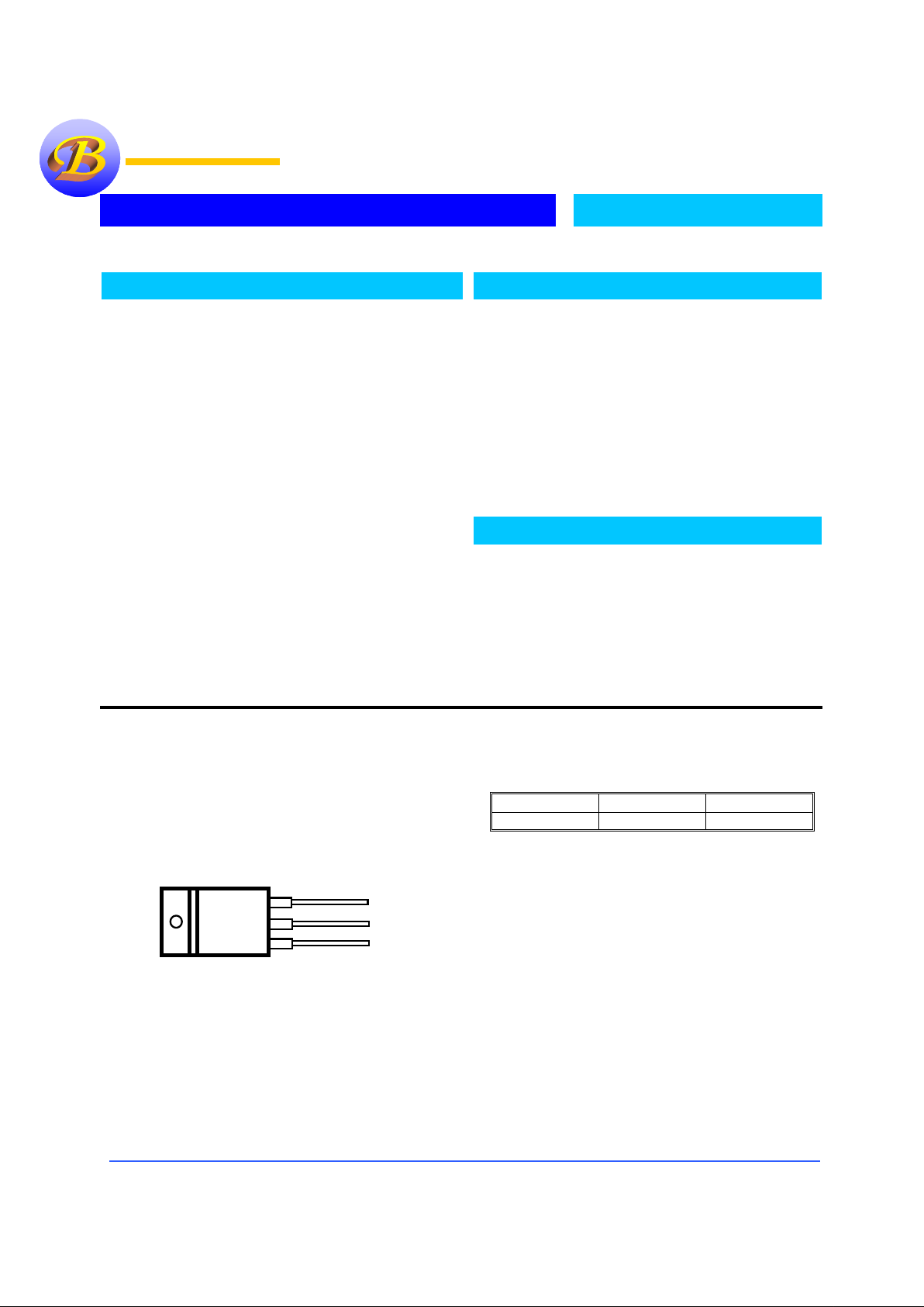
Pin Connection
Ordering Information
Devices Package Temp.
B1584T TO-220
0 °C to 70 °C
Description
The Bay Linear B1584 is Monolithic low power 8.0A
Adjustable and fixed NPN voltage regulator that are easy to
use with minimum external components. It is suitable for
applications requiring a well-regulated positive output voltage
with low input-output differential voltage requirements and
output voltage 1.5V, 2.5V, 3.0V, 3.3V, or 5V.
The B1584 Outstanding features include full power usage up
to 8.0Amp of load current internal current limiting and thermal
shutdown. Other fixed versions are also available consult with
factory.
The B1584 is offered in 3-pin TO-220 & TO-263 packages
compatible with other 3 terminal regulators. For 5A Low
dropout Regulator refer to the B1585 data sheet.
Features
• Adjustable Output Down to 1.2V
• Fixed Output Voltages 2.5V, 3.0V 3.3V,
and 5.0V
• Output Current of 8.0A
• Low Dropout Voltage 1.1V Typ.
• Current & Thermal Limiting
• Standard 3-Terminal Low Cost TO-220
•
Similar to industry Standard
LT1083/LT1584
Applications
• 3.3V to 2.5V for Pentium Processor
• SMPS Post Regulator
• High Efficiency “Green” Computer
Systems
• High Efficiency Linear Power Supplies
• 5V to 3.XXV fro Pentium Processor
• Battery Charger
Bay Li
Bay LiBay Li
Bay Linear
nearnear
near
Linear Excellence
Linear Excellen
ce
Linear Excellen
ce
Linear Excellence
Plastic Pac kage
TO-220
Front View
V
OUT
GND
V
IN
Plastic Pac kage
TO-220
Plastic Pac kage
TO-220
Front View
V
OUTVOUT
GND
V
INVIN

Bay Linear, Inc
2478 Armstrong Street, Livermore, CA 94550 Tel: (925) 989-7144, Fax: (925) 940-9556 www.baylinear.com
B1584
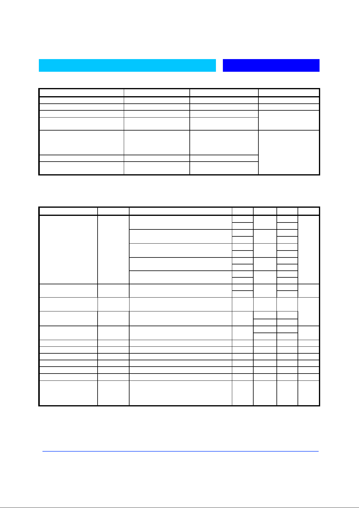
Absolute Maximum Rating
Parameter Symbol Value Unit
Maximum Input Voltage V
IN
7 V
Power Dissipation P
O
Internally Limited W
Thermal Resistance Junction to Case
θ
JC
3
Thermal Resistance Junction to
Ambient
θ
JA
50
°
C/W
Operating Junction
Temperature Range
Control Section
Power Transistor
T
J
0 to 125
0 to 150
Storage Temperature Range T
STG
-65 to 150
Lead Temperature (Soldering 10
Sec.)
T
LEAD
260
°
C
Electrical Characteristics
(VIN = 4.75V to 5.25V; IO = 10mA to 8.0Amp, unless otherwise specified)
Parameter Symbol Conditions MIN TYP MAX UNIT
1.485 1.515
0<I
OUT
<5A, 3.3V<VIN<7V, T= 25 °C
0<I
OUT
<5A, 3.3V<VIN<7V, Over Temp.
1.475
1.5
1.525
2.475 2.525
0<I
OUT
<5A, 4.0V<VIN<7V, T= 25 °C
0<I
OUT
<5A, 4.0V<VIN<7V, Over Temp.
2.460
2.5
2.540
2.970 3.030
0<I
OUT
<5A, 4.5V<VIN<7V, T= 25 °C
0<I
OUT
<5A, 4.5V<VIN<7V, Over Temp.
2.950
3.0
3.050
3.267 3.333
0<I
OUT
<5A, 4.8V<VIN<7V, T= 25 °C
0<I
OUT
<5A, 4.8V<VIN<7V, Over Temp.
3.247
3.3
3.353
4.950 5.050
Output Voltage V
O
0<I
OUT
<5A, 6.5V<VIN<7V, T= 25 °C
0<I
OUT
<5A, 6.5V<VIN<7V, Over Temp.
4.920
5.0
5.080
V
1.238 1.262 Reference Voltage V
ref
VIN<7V, 1.5V<VIN<5.75, 10mA<I
out
<5Amp
1.230
1.250
1.270
V
Line Regulation (1) REG
(line)
IO = 10mA, VIN =5V, T= 25 °C
0.04 0.2
0.08 0.40 Load Regulation (1) REG
(LOAD)
IO = 10mA, VIN =5V, T= 25 °C
%
1.0 Dropout Voltage V
D
T= 25 °C
Over Temperature
1.1 1.3
V
Minimum lo ad Current I
min
5.0 10 mA
Current Limit I
S
(Vin-V
out
)=3V 8 10 A
Ground Pin Current I
Q
VIN =5V 0 200 mA
Temperature Stability T
S
IO = 10mA, VIN =5V 0.5 %
Thermal Regulation
T= 25 °C, 30ms pulse
0.003 %/W
Ripple Rejection R
A
T= 25 °C, VIN =5V
60 80 dB
Thermal Resistance - TO-220 Junction to Tab
Junction to Ambient
DD Package Junction to Tab
Junction to Ambient
3.0
60
3.0
60
3.0
60
3.0
60
°
C/W
Note:
Output Switch tests are performed under pulsed conditions to minimize power dissipation
 Loading...