

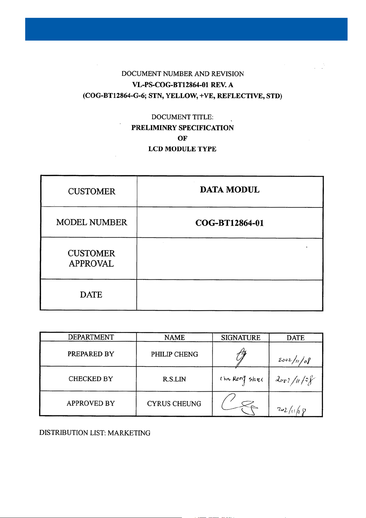
BTHQ 128064AVC-SRE-06-COG
Nov/2002
BA TRON
1/13
DATA MODUL AG Landsberger Str. 322 80687 München Tel.: 089/ 56017-0 Fax 089/ 56017-119
www.data-modul.de
BTHQ 128064AVC-SRE-06-COG
BA TRON
DOCUMENT REVISION HISTORY 1:
DOCUMENT
REVISION
FROM TO
A 2002.11.06 First Release.
DATE DESCRIPTION CHANGED
(Based on Test Specification:
VL-TS-COG-BT12864-XX, REV. A,
2002.10.28)
BY
PHILIP
CHENG
2/13
CHECKED
BY
R.S.LIN
DATA MODUL AG Landsberger Str. 322 80687 München Tel.: 089/ 56017-0 Fax 089/ 56017-119
www.data-modul.de

BTHQ 128064AVC-SRE-06-COG
BA TRON
Page No.
1. GENERAL DESCRIPTION 4
2. MECHANICAL SPECIFICATIONS 4
3. INTERFACE SIGNALS 7
4. ABSOLUTE MAXIMUM RATINGS 8
4.1
4.2 ENVIRONMENTAL CONDITION 8
5. ELECTRICAL SPECIFICATIONS 9
5.1 TYPICAL ELECTRICAL CHARACTERISTICS 9
5.2 TIMING SPECIFICATIONS 10
ELECTRICAL MAXIMUM RATINGS (Ta=25°C)
3/13
CONTENTS
8
DATA MODUL AG Landsberger Str. 322 80687 München Tel.: 089/ 56017-0 Fax 089/ 56017-119
www.data-modul.de
BTHQ 128064AVC-SRE-06-COG
BA TRON
1. General Description
• 128 x 64 dots STN Yellow Positive Reflective STD LCD Module.
• Viewing Direction: 6 O’clock.
• Driving duty: 1/65 Duty, 1/9 bias.
4/13
Preliminary Specification
of
LCD Module Type
Item No.: COG-BT12864-01
• ‘ULTRA CHIP’ UC1606 (COG) LCD Controller-Driver or equivalent.
• Logic Power Supply: +3V.
• FPC.
2. Mechanical Specifications
The mechanical detail is shown in Fig. 1 and summarized in Table 1 below.
Table 1
Parameter Specifications Unit
Outline dimensions 67.5(W) x 82.5(H) x 1.98(D) mm
Effective viewing area (V.A.) 60.00 MIN.(W) x 40.00 MIN.(H) mm
Active area (A.A.) 56.945(W) x 37.425(H) mm
Display format 128 x 64 dots
Dot size 0.43(W) x 0.57(H) mm
Dot spacing 0.015(W) x 0.015(H) mm
Dot pitch 0.445(W) x 0.585(H) mm
Weight: TBD grams
DATA MODUL AG Landsberger Str. 322 80687 München Tel.: 089/ 56017-0 Fax 089/ 56017-119
www.data-modul.de

BTHQ 128064AVC-SRE-06-COG
BA TRON
5/13
DATA MODUL AG Landsberger Str. 322 80687 München Tel.: 089/ 56017-0 Fax 089/ 56017-119
www.data-modul.de

BTHQ 128064AVC-SRE-06-COG
BA TRON
VLCD
VB0+
VB0-
VB1PS1
PS0
VB1+
VSS
VDD
D0(SCK),D1,
D2(SD1)~D7
8
/RD
/WR
CD
/RST
/CS0
DOT MATRIX LCD
CONTROLLER-DRIVER
'ULTRA CHIP'
UC1606
(COG)
OR EQUIVALENT
6/13
COG-BT12864G
LCD GRAPHIC DISPLAY
64
128 X 64 DOTS
128
Figure 2: Block diagram
DATA MODUL AG Landsberger Str. 322 80687 München Tel.: 089/ 56017-0 Fax 089/ 56017-119
www.data-modul.de

BTHQ 128064AVC-SRE-06-COG
BA TRON
3. Interface signals
Pin No. Symbol Description
1 CS0 Chip Select. In parallel mode and S8 mode, chip is selected when CS0=”L” and
CS1=”H”. When the chip is not selected, D[7:0] may be
high impedance.
2 RST When RST =”L”, all control registers are re-initialized by their default states. When
RST is not used, connect the pin to VDD.
3 CD Select Command or Display Data for read/write operation.
“L”: Command ”H”: Display data
4 WR
5 RD
6 D0(SCK)
7 D1
8 D2(SD1)
9 D3
10 D4
11 D5
12 D6
13 D7
14 VDD VDD1 is the digital power supply and it should be connected to a voltage source
15 VSS Ground.
17 PS0
18 PS1
16 VB1+
19 VB120 VB021 VB0+
22 VLCD Main LCD Power Supply. A by-pass capacitor CL is optional. When CL is used,
RD/WR(WR[1:0]) controls the read/write operation of the host interface.
In parallel mode, RD/WR(WR[1:0]) meaning depends on whether the interface is
in the 6800 mode or the 8080 mode. In serial interface modes, these two pins are
not used. Connect to VSS.
Bi-directional bus for both serial and parallel host interfaces.
In S8 and S9 mode, connect unused pins to VDD or VSS.
PS=1x Ps=0x
that is no higher than VDD2&3.
VDD2&3 is the analog power supply and it should be connected to the same power
source. Minimize the trace resistance for VDD2&3.
PS[1:0] Parallel/Serial.
Serial modes: “LL”: serial (S8) “LH”: serial (S9)
Parallel modes: “HL”: 8080 “HH”: 6800
LCD Bias Voltages. These are the voltage sources to provide SEG driving currents.
These voltages are generated internally. Connect capacitors of CBX value between
VBX+ and VBX–. The resistance of these four traces directly affects the SEG
driving strength of the resulting LCD module. Minimize the trace resistance is
critical in achieving high quality image.
connect CL between VLCD and VSS, and keep the trace resistance under 300
Ohm.
7/13
Table 2
D0 D0 SCK
D1 D1
D2 D2 SD1
D3 D3
D4 D4
D5 D5
D6 D6
D7 D7
DATA MODUL AG Landsberger Str. 322 80687 München Tel.: 089/ 56017-0 Fax 089/ 56017-119
www.data-modul.de

A
H
V
H
BTHQ 128064AVC-SRE-06-COG
BA TRON
4. Absolute Maximum Ratings
4.1 Electrical Maximum Ratings(Ta = 25 ºC)
Parameter Symbol Min. Max. Unit
Logic supply voltage VDD1 - VSS -0.3 +5.5 V
LCD generator supply voltage VDD2 - VSS -0.3 +5.5 V
Analog circuit supply voltage VDD3 - VSS -0.3 +5.5 V
LCD generated voltage VLCD -0.3 +15.5 V
Any input voltage Vin -0.3 VDD+0.3 V
8/13
Table 3
Note:
The modules may be destroyed if they are used beyond the absolute maximum ratings.
All voltage values are referenced to VSS = 0V.
VDD=VDD1=VDD2=VDD3.
4.2 Environmental Condition
Table 4
Item
Operating
Temperature
(Topr)
Storage
Temperature
(Tstg)
Remark
Min. Max. Min. Max.
mbient Temperature
umidity
0°C +50°C -10°C +60°C
95% max. RH for Ta ≤ 40°C
Dry
no condensation
< 95% RH for Ta > 40°C
ibration (IEC 68-2-6)
cells must be mounted
on a suitable connector
Shock (IEC 68-2-27)
alf-sine pulse shape
Frequency: 10 ∼ 55 Hz
Amplitude: 0.75 mm
Duration: 20 cycles in each direction.
Pulse duration : 11 ms
Peak acceleration: 981 m/s
2
= 100g
3 directions
3 directions
Number of shocks : 3 shocks in 3
mutually perpendicular axes.
DATA MODUL AG Landsberger Str. 322 80687 München Tel.: 089/ 56017-0 Fax 089/ 56017-119
www.data-modul.de

BTHQ 128064AVC-SRE-06-COG
BA TRON
5. Electrical Specifications
5.1 Typical Electrical Characteristics
At Ta = 25 °C, VDD = 3V±5%, VSS=0V.
Parameter Symbol Conditions Min. Typ. Max. Unit
Supply voltage
(Logic & booster)
LCD driving voltage VLCD-VSS 9.3 9.6 9.9 V
Supply Current
(Logic & booster)
9/13
Table 5
VDD-VSS 2.85 3.0 3.15 V
VIH ”H” level 0.8 VDD1 - - V Input signal voltage
” L” level - - 0.2VDD1 V
V
IL
IDD Character mode,
- 0.2 0.3 mA
Note 1
Note
(1) : There is tolerance in optimum LCD driving voltage during production and it will be within the
specified range.
DATA MODUL AG Landsberger Str. 322 80687 München Tel.: 089/ 56017-0 Fax 089/ 56017-119
www.data-modul.de

BTHQ 128064AVC-SRE-06-COG
BA TRON
5.2 Timing Specifications
Parallel bus timing characteristics (for 8080 MCU)
At Ta= 0°°°°C to +50°°°°C
10/13
DATA MODUL AG Landsberger Str. 322 80687 München Tel.: 089/ 56017-0 Fax 089/ 56017-119
www.data-modul.de

BTHQ 128064AVC-SRE-06-COG
BA TRON
Parallel bus timing characteristics (for 6800 MCU)
At Ta= 0°°°°C to +50°°°°C
11/13
DATA MODUL AG Landsberger Str. 322 80687 München Tel.: 089/ 56017-0 Fax 089/ 56017-119
www.data-modul.de

BTHQ 128064AVC-SRE-06-COG
BA TRON
Serial bus timing characteristics
At Ta= 0°°°°C to +50°°°°C
12/13
DATA MODUL AG Landsberger Str. 322 80687 München Tel.: 089/ 56017-0 Fax 089/ 56017-119
www.data-modul.de

BTHQ 128064AVC-SRE-06-COG
BA TRON
Serial bus timing characteristics
At Ta= 0°°°°C to +50°°°°C
13/13
DATA MODUL AG Landsberger Str. 322 80687 München Tel.: 089/ 56017-0 Fax 089/ 56017-119
www.data-modul.de
 Loading...