

Page 1
BARRETT 900 SERIES TRANSCEIVERS
Technical manual
Barrett 900 series HF transceivers and receivers
BARRETT 930, 950, 980 local control HF transceivers
BARRETT 930, 950 remote control ( trunk mount) HF transceivers
BARRETT 950M HF transceiver module
BARRETT 950MR HF receiver
BARRETT 940 HF portable transceiver
BARRETT COMMUNICATIONS©
© Barrett Communications
BCM90000/4
Head office: European office
Barrett Communications Pty Ltd Barrett Europe Limited
10 Port Kembla Drive, Bibra Lake WA 6163 19 Lenten Street
P O Box 1214, Bibra Lake WA 6965 Alton, Hampshire
AUSTRALIA GU34 1HG
Toll Free Tel: 1800 999 570 UNITED KINGDOM
Tel: (61-8) 9 434 1700 Tel: (44) 1420 542254
Fax: (61-8) 9 418 6757 Fax: (44) 1420 54337, P3
:
PAGE 1
Page 2

BARRETT 900 SERIES TRANSCEIVERS
1.0 Specifications ... ............ ............ ............ ............ ............ ............ ............ ............ ............ ............5
1.1 General Specifications... ............ ............ ............ ............ ............ ............ ............ ............5
1.2 Receiver Specifications . ............ ............ ............ ............ ............ ............ ............ ............7
1.3 Transmitter Specifications .......... ............ ............ ............ ............ ............ ............ ............8
2.0 Introduction....... ............ ............ ............ ............ ............ ............ ............ ............ ............ ............9
3.0 Overview .......... ............ ............ ............ ............ ............ ............ ............ ............ ............ ............11
3.1 Front Panel ....... ............ ............ ............ ............ ............ ............ ............ ............ ............11
3.2 Microprocessor PCB...... ............ ............ ............ ............ ............ ............ ............ ............11
3.3 RF/Audio PCB .. ............ ............ ............ ............ ............ ............ ............ ............ ............11
3.4 PA PCB ............ ............ ............ ............ ............ ............ ............ ............ ............ ............12
3.5 Remote Control Head .... ............ ............ ............ ............ ............ ............ ............ ............12
3.6 940 front panel .. ............ ............ ............ ............ ............ ............ ............ ............ ............12
3.7 940 connector transition PCB...... ............ ............ ............ ............ ............ ............ ............12
4.0 Technical description ..... ............ ............ ............ ............ ............ ............ ............ ............ ............13
4.1 Microprocessor PCB...... ............ ............ ............ ............ ............ ............ ............ ............13
4.1.2 Power supplies . ............ ............ ............ ............ ............ ............ ............ ............13
4.1.3 Reference oscillator (Standard) .. ............ ............ ............ ............ ............ ............13
4.1.4 Reference oscillator (High stability option) ............ ............ ............ ............ ............13
4.1.5 Microprocessor. ............ ............ ............ ............ ............ ............ ............ ............13
4.1.6 DDFS and VCO. ............ ............ ............ ............ ............ ............ ............ ............15
4.1.7 Selcall (if enabled).......... ............ ............ ............ ............ ............ ............ ............17
4.1.8 Audio mute........ ............ ............ ............ ............ ............ ............ ............ ............17
4.1.9 PA ALC controlvoltage PWR ADJ ............ ............ ............ ............ ............ ............18
4.2 RF / Audio PCB . ............ ............ ............ ............ ............ ............ ............ ............ ............19
4.2.1 RF section......... ............ ............ ............ ............ ............ ............ ............ ............19
4.2.1.1 .30 MHz Low passfilter, first mixer and 45 MHz IF amplifier.. ............ ............19
4.2.1.2 .Second mixer and bandpasscrystal filter.. ............ ............ ............ ............21
4.2.1.3 .Noise blanker.... ............ ............ ............ ............ ............ ............ ............21
4.2.1.4 .Noise gate......... ............ ............ ............ ............ ............ ............ ............21
4.2.1.5 .Second IF, AGC and demodulator............ ............ ............ ............ ............21
4.2.1.6 .Transmitand receive switching ... ............ ............ ............ ............ ............21
4.2.2 Audio section .... ............ ............ ............ ............ ............ ............ ............ ............21
4.2.2.1 .Audio path......... ............ ............ ............ ............ ............ ............ ............22
4.3 PA PCB ............ ............ ............ ............ ............ ............ ............ ............ ............ ............24
4.3.1 Gain control amp ............ ............ ............ ............ ............ ............ ............ ............24
4.3.2 Low pass filters . ............ ............ ............ ............ ............ ............ ............ ............24
4.3.3 ALC control ....... ............ ............ ............ ............ ............ ............ ............ ............24
4.3.4 Over-voltage and reverse voltage protection......... ............ ............ ............ ............24
4.3.5 Auxiliary antenna socket ............ ............ ............ ............ ............ ............ ............24
4.3.6 Receiver RF amplifier..... ............ ............ ............ ............ ............ ............ ............24
4.3.7 Power supply regulators. ............ ............ ............ ............ ............ ............ ............24
4.4 Front panel........ ............ ............ ............ ............ ............ ............ ............ ............ ............26
4.4.1 LCD and status LED's .... ............ ............ ............ ............ ............ ............ ............26
4.4.2 Keypad ............ ............ ............ ............ ............ ............ ............ ............ ............26
4.4.3 Backlighting ...... ............ ............ ............ ............ ............ ............ ............ ............26
4.4.4 Microphone....... ............ ............ ............ ............ ............ ............ ............ ............26
4.4.5 Volumecontrol and On/Off switch ............ ............ ............ ............ ............ ............26
4.5 Remote control head ...... ............ ............ ............ ............ ............ ............ ............ ............28
5.0 Maintenance..... ............ ............ ............ ............ ............ ............ ............ ............ ............ ............30
5.1 Introduction....... ............ ............ ............ ............ ............ ............ ............ ............ ............30
5.2 Printed Circuit Board (PCB)maintenance ............ ............ ............ ............ ............ ............30
5.3 Component replacement ............ ............ ............ ............ ............ ............ ............ ............30
5.4 CMOS devices.. ............ ............ ............ ............ ............ ............ ............ ............ ............31
5.5 Transmitter power amplifier maintenance precautions....... ............ ............ ............ ............31
5.6 PCB access ...... ............ ............ ............ ............ ............ ............ ............ ............ ............31
5.6.1 930 - 950 - 980 transceivers......... ............ ............ ............ ............ ............ ............31
5.6.2 940 transceivers ............ ............ ............ ............ ............ ............ ............ ............31
5.6.3 930 - 950 remote control head ..... ............ ............ ............ ............ ............ ............31
PAGE 2
Page 3

BARRETT 900 SERIES TRANSCEIVERS
5.7 Fault diagnosis.. ............ ............ ............ ............ ............ ............ ............ ............ ............32
5.7.1 General ............ ............ ............ ............ ............ ............ ............ ............ ............32
5.7.2 Transceiver will not power up ...... ............ ............ ............ ............ ............ ............33
5.7.3 Transceiver will not receive butdisplays OK .......... ............ ............ ............ ............35
5.7.3.1 No receiver noise atall ... ............ ............ ............ ............ ............ ............35
5.7.3.2 Receive noise present, butdoes not receive.......... ............ ............ ............35
5.7.3.4 Transceiver turns on but displays"Barrett 900 Transceiver" only. .... ............35
5.7.4 Transceiver turns on, internal voltagesare normal, but no LCD display......... ............36
5.7.5 Main microprocessor faults ......... ............ ............ ............ ............ ............ ............36
5.7.6 VCO faults ........ ............ ............ ............ ............ ............ ............ ............ ............37
5.7.7 Transmitter faulty ........... ............ ............ ............ ............ ............ ............ ............37
5.7.8 Replacement of PA output and drivertransistors ... ............ ............ ............ ............38
5.8 Adjustments...... ............ ............ ............ ............ ............ ............ ............ ............ ............40
5.8.1 Front panel........ ............ ............ ............ ............ ............ ............ ............ ............40
5.8.2 Microprocessor PCB...... ............ ............ ............ ............ ............ ............ ............40
5.8.2.1 Reference oscillator setup (Standardoscillator) .... ............ ............ ............40
5.8.2.2 Reference oscillator setup (Highstability oscillator)............ ............ ............40
5.8.2.3 VCO frequency adjustment ......... ............ ............ ............ ............ ............40
5.8.2.4 Carrier Insertion oscillator peaking........... ............ ............ ............ ............40
5.8.2.5 VCO Low pass filter........ ............ ............ ............ ............ ............ ............40
5.8.2.6 DAC Low pass filter........ ............ ............ ............ ............ ............ ............41
5.8.3 RF/ Audio PCB .. ............ ............ ............ ............ ............ ............ ............ ............41
5.8.3.1 Input low pass filter......... ............ ............ ............ ............ ............ ............41
5.8.3.2 45MHz IF Filter.. ............ ............ ............ ............ ............ ............ ............41
5.8.3.3 IF Inductors....... ............ ............ ............ ............ ............ ............ ............42
5.8.3.4 Noise blanker potentiometer ....... ............ ............ ............ ............ ............42
5.8.3.5 Carrier rejection potentiometer.... ............ ............ ............ ............ ............42
5.8.3.6 Transmit drive level set potentiometer...... ............ ............ ............ ............42
5.8.3.7 455Khz IF ......... ............ ............ ............ ............ ............ ............ ............42
5.8.4 PA PCB ............ ............ ............ ............ ............ ............ ............ ............ ............42
5.8.4.1 Driver bias setup ............ ............ ............ ............ ............ ............ ............42
5.8.4.2 PA bias setup .... ............ ............ ............ ............ ............ ............ ............42
5.8.4.3 Power level adjustment .. ............ ............ ............ ............ ............ ............43
5.3.4.4 Programmable links ....... ............ ............ ............ ............ ............ ............43
6.0 Software programming and options ......... ............ ............ ............ ............ ............ ............ ............44
6.1 Barrett 930 transceivers . ............ ............ ............ ............ ............ ............ ............ ............44
6.2 Barrett 940 transceivers . ............ ............ ............ ............ ............ ............ ............ ............44
6.3 Barrett 950 transceivers . ............ ............ ............ ............ ............ ............ ............ ............44
6.4 Barrett 980 transceivers . ............ ............ ............ ............ ............ ............ ............ ............44
7.0 Internal jumper settings ............ ............ ............ ............ ............ ............ ............ ............ ............45
7.1 Standard jumpers locations ........ ............ ............ ............ ............ ............ ............ ............45
7.2 Configuring antenna connectors . ............ ............ ............ ............ ............ ............ ............45
8.0 Internal options ............ ............ ............ ............ ............ ............ ............ ............ ............ ............46
8.1 Internal scrambler option ............ ............ ............ ............ ............ ............ ............ ............46
8.2 Internal GPS receiver option ....... ............ ............ ............ ............ ............ ............ ............48
8.3 Internal ALE option P/NBCA95001 and BCA95002 ........... ............ ............ ............ ............48
9.0 Features and configurations uniqueto transceiver models . ............ ............ ............ ............ ............49
9.1 Barrett 950 transceivers fittedwith high stability option - P/N BC95001 and BC95003 ............49
9.2 Barrett 950M transceiver module- P/N BC95004 .. ............ ............ ............ ............ ............49
9.3 Barrett 950MR receivers ............ ............ ............ ............ ............ ............ ............ ............49
9.4 Barrett 940 man-pack..... ............ ............ ............ ............ ............ ............ ............ ............50
9.4.1 940 ancillary components ........... ............ ............ ............ ............ ............ ............50
9.4.1.1 110 to 240VAC inputcharger supply Barrett P/N BCA94012 ........... ............50
9.4.1.2 Charge regulator suit 13Ah NiMH battery 12V DC input P/N BCA94021 ...50
9.4.1.3 940 multiple-use distribution unitBarrett P/N BCA94010 .... ............ ............51
9.4.1.4 940 automatic antenna tuner....... ............ ............ ............ ............ ............51
9.5 Barrett 980 GMDSS transceiver.. ............ ............ ............ ............ ............ ............ ............52
PAGE 3
Page 4

BARRETT 900 SERIES TRANSCEIVERS
10.0 Accessory interface unit - P/N BCA90016 ............ ............ ............ ............ ............ ............ ............53
11.0 Auxiliary connector ........ ............ ............ ............ ............ ............ ............ ............ ............ ............54
11.1 Barrett 980 and Barrett 950 transceivers .. ............ ............ ............ ............ ............ ............54
11.2 Barrett 930 transceivers . ............ ............ ............ ............ ............ ............ ............ ............55
11.3 Barrett 940 manpack transceivers............ ............ ............ ............ ............ ............ ............56
12.0 Circuit diagrams, overlays and parts lists.. ............ ............ ............ ............ ............ ............ ............57
Active component outlines .......... ............ ............ ............ ............ ............ ............ ............ ............57
RF/Audio PCB overlay ... ............ ............ ............ ............ ............ ............ ............ ............ ............58
RF/Audio schematic....... ............ ............ ............ ............ ............ ............ ............ ............ ............59
RF/Audio parts List - showing optional narrow filtercomponents. .... ............ ............ ............ ............61
Microprocessor PCB overlay....... ............ ............ ............ ............ ............ ............ ............ ............72
Microprocessor schematic .......... ............ ............ ............ ............ ............ ............ ............ ............73
Microprocessor parts list ............ ............ ............ ............ ............ ............ ............ ............ ............75
PA PCB overlay. ............ ............ ............ ............ ............ ............ ............ ............ ............ ............87
PA schematic .... ............ ............ ............ ............ ............ ............ ............ ............ ............ ............89
PA parts list ....... ............ ............ ............ ............ ............ ............ ............ ............ ............ ............91
Front panel PCB overlay ............ ............ ............ ............ ............ ............ ............ ............ ............99
Front panel schematic .... ............ ............ ............ ............ ............ ............ ............ ............ ............100
Front panel parts list....... ............ ............ ............ ............ ............ ............ ............ ............ ............101
Remote control head PCB overlay ........... ............ ............ ............ ............ ............ ............ ............103
Remote control head schematic.. ............ ............ ............ ............ ............ ............ ............ ............104
Remote control head parts list ..... ............ ............ ............ ............ ............ ............ ............ ............105
Scrambler PCB overlay Barrett P/N BCA94031 ... ............ ............ ............ ............ ............ ............108
Scrambler schematic ..... ............ ............ ............ ............ ............ ............ ............ ............ ............109
Scrambler parts list ........ ............ ............ ............ ............ ............ ............ ............ ............ ............110
GPS/ALE motherboard overlay ... ............ ............ ............ ............ ............ ............ ............ ............111
GPS/ALE motherboard schematic ........... ............ ............ ............ ............ ............ ............ ............112
GPS/ALE motherboard parts list . ............ ............ ............ ............ ............ ............ ............ ............113
950MR Low Pass Filter/Power PCB overlay.......... ............ ............ ............ ............ ............ ............114
950MR Low Pass Filter/Power PCB schematic ..... ............ ............ ............ ............ ............ ............115
950MR Low Pass Filter/Power PCB partslist ........ ............ ............ ............ ............ ............ ............117
980PSU DC/DC switch mode power supplyPCB overlay ... ............ ............ ............ ............ ...........121
980PSU DC/DC switch mode power supplyschematic ...... ............ ............ ............ ............ ............122
980PSU DC/DC switch mode power supplyparts list.......... ............ ............ ............ ............ ............123
900 series final assembly parts lists.......... ............ ............ ............ ............ ............ ............ ............125
930, 940, 950, 980 hand microphoneschematic.... ............Barrett P/N BCA90003 ... ............ ............133
930, 950, 980 cloning cable schematic..... ............ ............Barrett P/N BCA90024 ... ............ ............134
930, 950, 980 programming cable schematic ........ ............Barrett P/N BCA90023 ... ............ ............135
940 chassis explosion diagram ... ............ ............ ............ ............ ............ ............ ............ ............136
940 final assembly parts list......... ............ ............ ............ ............ ............ ............ ............ ............137
940 connector transition PCB overlay ...... ............ ............ ............ ............ ............ ............ ............139
940 connector transition schematic.......... ............ ............ ............ ............ ............ ............ ............140
940 connector transition parts list ............ ............ ............ ............ ............ ............ ............ ............141
940 automatic antenna tuner PCB overlay ............ ............Barrett P/N BCA94009 ... ............ ............142
940 automatic antenna tuner ... ............ ............Barrett P/N BCA94009 ... ............ ............143
940 auto tuner PCB parts list.......... .......... ............ ............ ............ ............ ............ ............ ............146
940 automatic antenna tuner final assemblyparts list (Drab Olive, Periwinkle) .......... ............ ............147
940 tuner front panel PCB overlay............ ............ ............ ............ ............ ............ ............ ............148
940 tuner front panel PCB schematic ....... ............ ............ ............ ............ ............ ............ ............149
940 ATU front panelPCB parts list ............ ............ ............ ............ ............ ............ ............ ............150
940 multiple-use distribution unit schematic .......... ............Barrett P/NBCA94010 ... ............ ............151
940 multiple-use distribution unit parts list ............ ............BarrettP/N BCA94010... ............ ............152
940 charge reg. 13Ah / 12VDC input PCB overlay . ............Barrett P/N BCA94021 ... ............ ............153
940 charge reg. 13Ah / 12VDC input PCB schematic .........Barrett P/N BCA94021 ... ............ ............154
940 battery charger PCB parts list ............ ............ ............Barrett P/N BCA94021 ... ............ ............157
940 transceiver cloning cable schematic .. ............ ............Barrett P/N BCA94014 ... ............ ............160
940 handset lightweight tactical schematic............ ............Barrett P/N BCA94004 ... ............ ............161
940 transceiver mic schematic ............ ............ ............Barrett P/N BCA94013 ... ............ ............162
940 programming cable schematic .......... ............ ............Barrett P/N BCA94013 ... ............ ............163
schematic
PAGE 4
Page 5

1.0 Specifications
1.1 General Specifications
BARRETT 900 SERIES TRANSCEIVERS
Equipment GMDSS transceiver.
Transmit frequency range 1.6 MHz to 30 MHz (continuous)
Receive frequency range 500 kHz to 30 MHz (continuous)
Channel capacity 980 local and remote control models, 950 local and remote control
Frequency resolution 10 Hz program mode
Frequency stability Standard ±50 Hz (0 to +55 C)
BARRETT 980
BARRETT 950 BARRETT
930 BARRETT 950M
transceiver local and remote control models
transceiver module
BARRETT 950MR
specifications and descriptions)
BARRETT 940
(adjustable))
models, 950R and 950MR1 receivers and - Up to
450 programmable channels (simplex or semi-duplex)
930 local and remote control models - Up to 20 programmable channels
(simplex or semi-duplex)
1 Hz tuneable receiver (940, 950 and980 transceivers)
Optional ±10 Hz (-15 C to +55 C)(Standard 980)
transceiver local and remote control models
receiver module (disregard references to transmit
man-pack transceiver (power output limited to 10 - 35 W
940 man-pack model
°°
°°
Intermediate frequencies 45 MHzand 455kHz (double conversion)
Operating modes J3E (USB, LSB)
H3E (AM)
J2A (CW)
J2B (AFSK) standard filter (980, 950 local and remote control models
only)
J2B (AFSK) narrow filter option (980, 950 local and remote control models
only)
Operating temperature -30 C to +55 C
Humidity 95% relative, non condensing
Display system Supertwist backlit LCD matrix, 16 characterx 2 line
Controls 20 key keypad (illuminated), analogue power/volume
Supply voltage - 13.8 VDC + 20% /- 10% (negative ground)
Current consumption local control models 840 mA receive
receive. remote control models 860 mA receive
°°
930, 940, 950
Polarity protected. Over voltage protected
980
- 24 VDC +20% / -10% galvanically isolated from transceiver (using
matching, switch mode power supply)
930, 950
930, 950
980
(24V) 450 mA receive
940
595 mA receive
Antenna Impedance 50 unbalanced
Compass Safe Distance GMDSS transceiver 2 metres
W
980
PAGE 5
Page 6

BARRETT 900 SERIES TRANSCEIVERS
Weight 3.6 Kg.
Dimensions 250 mm x 75 mm x300 mm
930, 950 and 980
950MR1
portable transceiver 3.9 Kg.
940
13 Ah NiMH battery pack 2.7Kg
940
Optional 940
automatic antenna tuner 1.8 Kg.
3.2Kg.
930 - 950 - 980
transceiver - no battery 275 mm x97 mm x 210 mm
940
transceiver and battery 275 mm x 97 mm x310 mm
940
transceiver, battery and top case 275 mm x 97mm x 405mm
940
Optional 940
automatic antenna tuner 275 mm x 53 mm x 210 mm
Selcall System Based on CCIR 493-4
Scan Types Selcall, Voice(syllabic), AGCderived signal level.
Scan Channels Two tables,programmable by channel.
Scan Rate Selcall Scan - Fixed at 500ms.
Non Selcall scan - Adjustable from100 ms to 5 secs
.
PAGE 6
Page 7

BARRETT 900 SERIES TRANSCEIVERS
1.2 Receiver Specifications
Sensitivity 0.256uV (-119dBm) for 10dB SINAD- J3E Mode (With RFpre-amp on)
Selectivity J3E -1kHz and+ 4kHz better than 60dB
Selectivity F1B (optional) -500Hz and+ 500Hzbetter than 45dB
Desensitisation -1kHz and + 4kHz better than 60dB
-10kHz and +10kHz better than71dB
-20kHz and +20kHz better than80dB
-50kHz and +50kHz better than87dB
The level of an unwanted signal above the level of a wanted signal that will
reduce the SINAD of the wanted signal producing 10dB SINAD to 7dB
SINAD
Image rejection Better than 76dB
Spurious response ratio Better than 70dB
Cross modulation -20kHz and +20kHz better than82dB
The level of an unwanted signal that is 30% AM modulated and at
20kHz above the level of a wanted signal that is producing 10dB SINAD
that will cause this wanted signalSINAD to reduce by 3dB
Blocking -20kHzand +20kHz better than 80dB
The level of an unwanted signal above the level of a wanted signal that will
reduce the SINAD of the wanted signal producing 10dB SINAD to 7dB
SINAD
Intermodulation 85dB - the level ofan unwantedsignal in relation to a wanted signal.
Inband IMD Greater than 34dB
Clarifier range Receive only 1Hz steps up to±1kHz (dependant on configuration).
AGC efficiency Less than 6.0 dB variation with an input signal of 6uV(-91.4dBm) to
3V(+22.5dBm).
Audio Output 4W into 4 Ohms,2W into8 Ohms at less than 5% distortion
Audio output impedance 2 to 80 Ohms
Audio response Less than 6dB variation from 350Hz to 2750Hz
Audio distortion Less than 5%at ratedpower J3E mode
Input protection Better than 30VRMS froma 50 ohm source
PAGE 7
Page 8

1.3 Transmitter Specifications
BARRETT 900 SERIES TRANSCEIVERS
RF Output Power 100 W PEP two tone ±1 dB
Duty Cycle 100% two-tone input signal with fanoption
Protection Safe under all load conditions, thermal protection against excessive power
Sideband suppression Better than -65dB below PEP
Harmonic suppression Betterthan -60dBbelow PEP
Carrier suppression Better than -60dBbelow PEP
Spurious emission Better than -60dB below PEP
Intermodulation products Better than-31dB belowPEP (25dB below two tone peak)
930 - 950
125 W PEP voice ± 1dB
or
10 W PEP twotone ±1 dB
12 W PEP voice ± 1dB
980
940
(portable) 25 W two tone 10 - 35 W PEP (factory set to user
930, 950,980
940
(portable) 25% voice duty cycle
transistor temperatures.
100 W PEP two tone ±1.5dB
requirement)
Audio frequency response Less than 6 dB variation 350Hz to 2750 Hz
Current consumption Voiceaverage less than 9Amps typical
930, 950, 980
940
Twotone less than 15Amps typical
Voiceaverage less than 5Amps typical.
Twotone less than 9Amps typical.
PAGE 8
Page 9

2.0 Introduction
This technical manual covers the Barrett 950 local and remote control transceiver, the Barrett 980 GMDSS
transceiver, the Barrett 940 man-pack transceiver, the Barrett 930 local and remote control transceiver, the
Barrett 950M transceiver module and the 950MR receivers. They have largely identical hardware and only
vary by key function and operational software and in the case of the 940 the mounting hardware and
enclosure.
BARRETT 900 SERIES TRANSCEIVERS
PAGE 9
Page 10
BARRETT 900 SERIES TRANSCEIVERS
PAGE 10
DRAWING NUMBER
900B64A3.PCB
SCALE
NTS
DRAWN
DJS (PE)
DRAWING TITLE
BARRETT 900
SYSTEM BLOCK DIAGRAM
DATE
25-1-99
DIMENSIONING
DESIGNED
PMW
ECN REFERENCE
BARRETT PART NO
SHEET
1OF1
Page 11

3.0 Overview
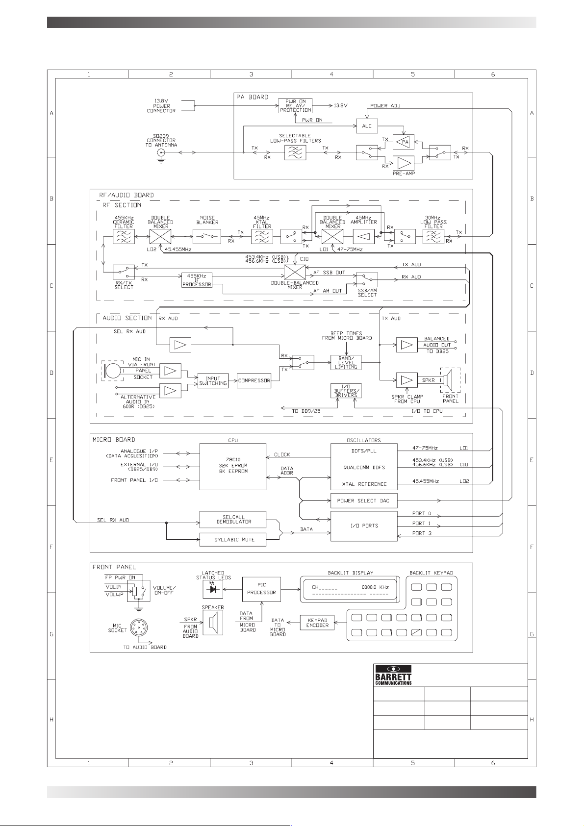
All 900 series transceivers and receivers are made up of several common building blocks. Apart from the
940 man-pack transceiver they are all constructed with a common chassis. This manual deals with each
module and has a separate section describing sections of transceivers and receivers that are unique
to that transceiver or receiver.
The 980/950/930/ local control transceivers arecomprised of the following four modules:-
*Front Panel *MicroprocessorPCB
*PA PCB *RF/Audio PCB
The 950/930 remote control transceivers arecomprised of the following four modules:-
*Microprocessor PCB *PA PCB
*RF/Audio PCB Remote control head and interface cable
The 940 man-pack comprises thefollowing six modules:-
*Microprocessor PCB *PA PCB
*RF/Audio PCB *Front panel
*Connector transition PCB
BARRETT 900 SERIES TRANSCEIVERS
*
3.1 Front Panel
The backlit keypad allows entry of channel number, transmit frequency, receive frequency, mode, Selcall,
power, scan, ATU option and customer specific information. A 2 line x 16 character backlit LCD display
annunciates the channel frequency and indicateswhich functions have been selected on thischannel.
Numerous other status displays are optionally available. On the left hand side of the display 5 status LED's
indicate the currentmode ofthe transceiver. A red LED is illuminated in transmit, a greenLED inreceive and
three yellow LED's indicate which of the three modes, USB, LSB or AM has been selected (J3E, H3E, F1B
on the 980 transceiver). A rotary volume control and on/off switch and a Mylar cone speaker are also
included on the front panel. The microphone which incorporates press to talk and channel up/down buttons,
plugs into an 8 pin socket on the front panel. Note:- The standard microphone has a jumper in it (refer to the
microphone diagrams) that enables the front panel speaker, the handset does not have this jumper thus
disabling the speaker.
3.2 Microprocessor PCB
The Microprocessor PCB is the central control of the transceiver. This PCB also contains the Direct Digital
Frequency Synthesis (DDFS) system which generates all local oscillator injection frequencies, the Selcall
demodulator and the audio syllabic mutesensing circuit.
3.3 RF/Audio PCB
The RF/Audio PCB contains the receiver and transmitter exciter, the audio processor section and general
interface to theoutside of the transceiver. The receiver employs a double conversion superhet design with a
high dynamic range. All receiver signals are processed through either a single sideband filter which has a
passband of 2.4KHz or in the case of AFSK (J2B) signals, through a narrow sideband filter with a passband
of 500Hz. A product detector is used to demodulate all single sideband signals, whilst an envelope detector
is used to demodulate AM signals. An effective noise blanker, employing a separate pulse receiver, is
provided which may be switched onor off as required.
There is a great deal ofcommonality between receive and transmit paths inboth the R.F. and audiocircuits.
In transmit, audiofrom the microphone, the auxiliary input or the remote head ispassed to an automatic level
control circuit which amplifies and maintains a constant modulating signal with considerable variations in
input signal level. This maintains anadequate modulation level in all circumstances.
On receive, the signal is amplified and fed to a mute circuit. Both receive and transmit audio share a
common path up to the volumecontrol. The RS-232 computerinterface islocated on the RF/Audio PCB.
PAGE 11
Page 12

BARRETT 900 SERIES TRANSCEIVERS
3.4 PA PCB
The PA PCB raises the power levelto 25W, 100 or 125 W PEP depending on the setup of the power amplifier
and the model. Seven low pass filters provide harmonic rejection over the full frequency range, reduce
receiver LO radiation and enhance image rejection of the receiver. Also resident on the PA PCB is power
protection circuitry guarding against over-voltage, reversevoltage and low voltage supplies.
ALC protection and regulation of the transmitter power output will protect the transceiver from reactive loads
plus open and short circuit antennaconnections.
3.5 Remote Control Head
The remote head can be operated up to 20 metres from any 900 series transceiver (three remote head
interface cables joined together).
The control cable is connected to the remote head via a 9 pin "D" connector. The loudspeaker output being
by a 3.5 mmjack socket.
The remote head contains its own microprocessor to drive the display, but otherwise contains no controlling
intelligence. The remote head firmware is the same for 930, 950 and 980 transceivers - the only difference,
in the heads, being thefront panel membrane and key functions.
3.6 940 front panel
The 940 front panel is a Barrett 900 series remote head fitted into an "O" ringed aluminium front panel. The
front half of the remote head plastic front panel is retained the rear half is removed. A special loom is fitted to
the remote head PCB to connect to the RF/Audio PCB. Also fitted to the front panel is a connector transition
PCB described below. In addition to the normal commercial microphone connector on the remote control
head panel there are two military connectors. The 5 pin panel socket provides a handset connection while
the other 8 pin panel plug provides interface signals to the 940 auto tuner, serial communications for
programming and cloning, CW key andpower connections.
3.7 940 connector transition PCB
The connector transition PCB provides a microphone amplifier for the handset and transition from the IDC
connector to the military connectors.
PAGE 12
Page 13

4.0 Technical description
4.1 Microprocessor PCB
The Microprocessor PCB incorporates the microprocessor unit which controls the transceiver system, the
synthesiser, which provides three stable local oscillator sources, the selcall encoder/decoder which
generates and demodulates selcall signals, andthe audio syllabic mute and transmitter powercontrol.
4.1.2 Power supplies
The transceiver has several internal voltage regulators to obtain +5 volt and +10 volt supplies used
throughout the transceiver. Where lowest power consumption is required, as in the 940 man-pack, some of
these have a switch mode regulatorto replace the normally fitted linear regulators.
On the microprocessor PCB, U19 and U20 can be replaced by a single switch-mode regulator U36. Other
minor components that need to beadded are L3, L6 C118, C119, C117, and C121.
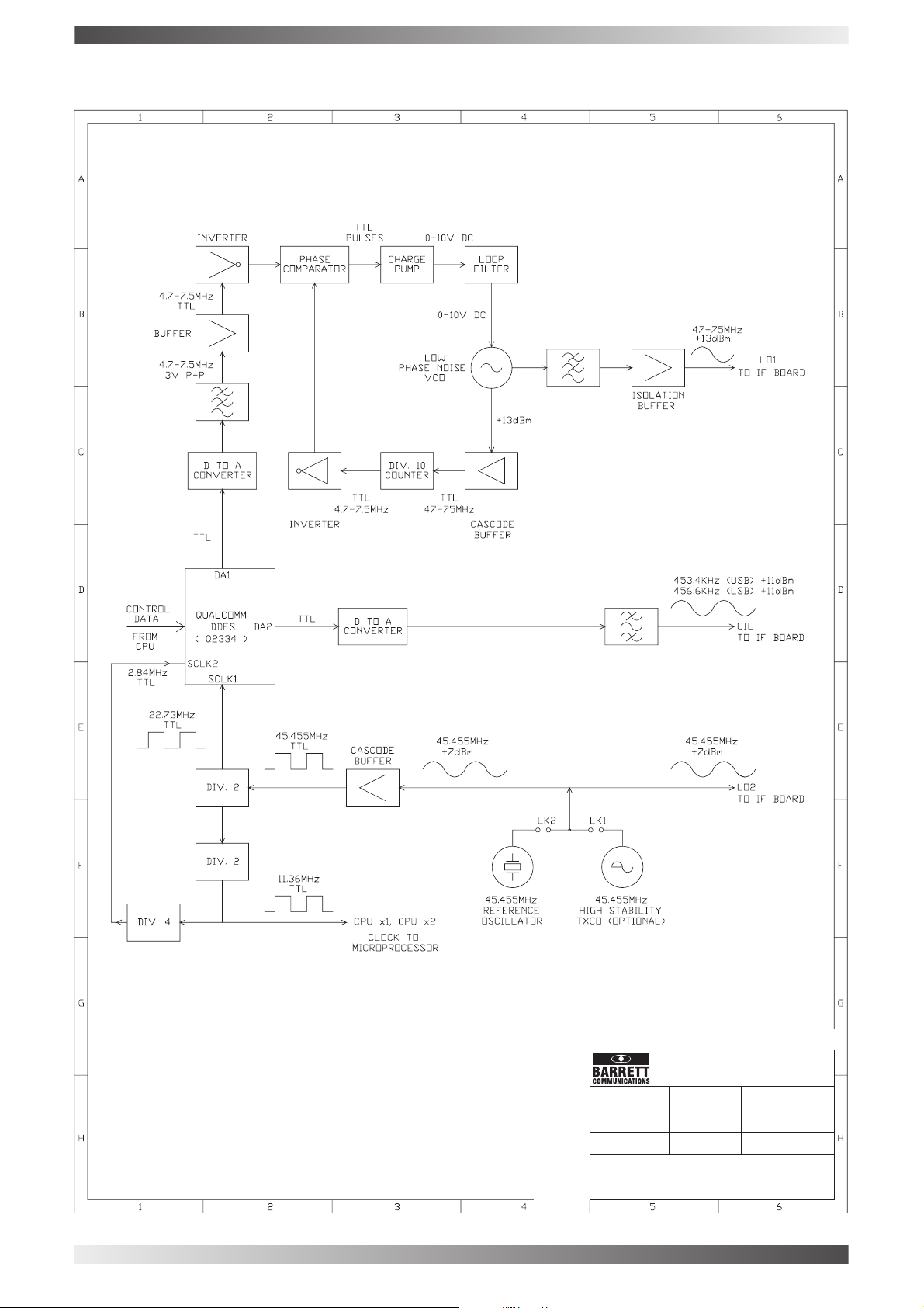
4.1.3 Reference oscillator (Standard)
The reference oscillator at 45.455 MHz is the master clock which determines the frequency and timing of all
other synchronous events in the transceiver. It consists of active devices Q13 and Q14 configured as a
Butler oscillator. L16 is set to cancel the crystal stray capacitance and L15 resonates with C132, C133 and
C137, C146 to provide fine frequency trimming. The oscillator is trimmed to 1ppm and an oven maintains a
constant crystal temperature. The output of the reference oscillator is fed direct to the second mixer on the
RF/Audio PCB via TP35 and is buffered prior to routing to the digital section by Q10 and Q11. These are
configured in cascode to minimise reverse coupling. Further buffering is obtained from inverter U31:A prior
to feeding the cascade flip flops U32:A and U32:B. These devices provide a 1:1 duty cycle clock for the
DDFS chip U7 at 22.72 MHz and the microprocessor U1 at 11.36 MHz. A further divider U13 yields 2.84
MHz clock for the Carrier Insertion Oscillator generation by the DDFS. Link LK2 must be IN and LK1 must be
OUT for the standard oscillator.
BARRETT 900 SERIES TRANSCEIVERS
4.1.4 Reference oscillator (High stability option)
The reference oscillator at 45.455 MHz is the master clock which determines the frequency and timing of all
other synchronous events in the transceiver. It consists of either a modular TXCO or DCXO oscillating at
45.455 MHz. The oscillator frequency is trimmed using the adjustment on the top of the can. The output of
the TCXO is buffered by Q20, then fed direct to the second mixer on the RF/Audio PCB via TP35 and is
buffered prior to routing to the digital section by Q10 and Q11. These are configured in cascode to minimise
reverse coupling. Further buffering is obtained from inverter U31:A prior to feeding the cascade flip flops
U32:A and U32:B. These devices provide a 1:1 duty cycle clock for the DDFS chip U7 at 22.72 MHz and the
microprocessor U1 at 11.36 MHz. A further divider U13 yields 2.84 MHz clock for the Carrier Insertion
Oscillator generation in the DDFS. Link LK2 must be OUT and LK1 must be IN for the high stability oscillator
option.
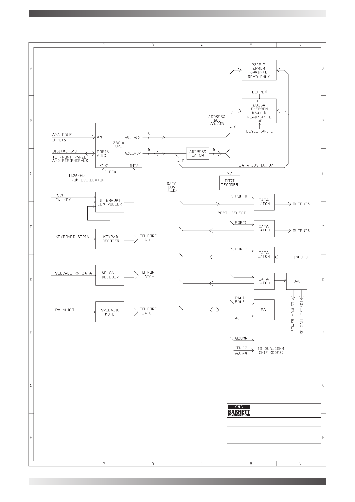
4.1.5 Microprocessor
The microprocessor U1 is the device which executes the control program for the transceiver. It executes
instructions stored in EPROM U4 and stores and reads non-volatile data from EEPROM U5. These are
connected via a sixteen line bus which has low order address and data multiplexed on the same eight lines.
The low address is de-multiplexed using octal latch U2. A security PAL U40 is also fitted on the data bus to
permit configuration security.
Two parallel output ports U15 (I/O Port 1) and U16 (I/O Port 0) handle static and slow logic signals from
microprocessor. These include PA filter select lines, Audio / IF control signals such as PTT, AM on and NB
on, Mic Disable, Speaker clamp andMute and ATU control signalsTune Clock and Scan Data.
U14 (I/O port 3) is used to input parallel data from U35, a PWM decoder used to input key PCB data from the
front panel and remote head.
Decoding for all these peripheral devices is provided by 3 to 8 decoder U6 along with U3 and U11. Shift
register U17 ensures that the timingfor the EEPROM operation is correct.
PAGE 13
Page 14
BARRETT 900 SERIES TRANSCEIVERS
PAGE 14
SYSTEM BLOCK DIAGRAM
DRAWING NUMBER
900B61A2.PCB
SCALE
NTS
DRAWN
GMH
DRAWING TITLE
DATE
DIMENSIONING
DESIGNED
BARRETT 900 MICRO BOARD
MICROCONTROLLER
5-8-98
PHW
ECN REFERENCE
BARRETT PART NO
SHEET
1OF1
Page 15

BARRETT 900 SERIES TRANSCEIVERS
The microprocessor has four sets ofports of its own used as follows:-
AN0 to AN7
signal strength using voltage AGC, synthesiser lock state using voltage VCO Lock and battery voltage
utilising a voltage derived from a voltage divider consisting of R2 and R35. AN5 and AN6 are used to
measure voltages used to set up the selcall VCO tuning during the startup sequence. AN7 is used for
internal chassis temperature measurement, provided by sensor TS1, which is used for PA ALC trimming at
high temperatures.
CO1, CO0, CI, TO, INT2, SCK,RXD, TXD, PTTIN, CW KEY, ALESEN, GPSEN
CO1 and CO0are counter/timer ports used to generate selcall transmit and alarm tones.CI and TO combine
to decode thereceived selcallpre -ambleand data stream. INT2 is the main interrupt processing PTTIN and
CW KEY, SCK is unused. RXD and TXD are the external RS-232 serial ports. RXD and TXD are routed by
U44 and combinations of signals ALESEN and GPSEN to input and output data to and from an internally
fitted ALE controlleroption, aswell as inputting data from either an external or internal GPS receiver. RESET
ALE is used to reset theALE controller option when fitted.
. These analogue input ports monitor transmit VSWR using voltages SWR+ and SWR-, receive
PB0 to PB7
Stop and Mute state.
PA0 to PA7
ALARM DATA.
Interrupts
KEY are latched by signal ICP from the microprocessor. A magnitude comparator U25 compares the lines
with their previous state and requestsan interrupt via INT2 if there isa state change.
4.1.6 DDFS and VCO
The synthesiser employs a Direct Digital Frequency Synthesiser integrated circuit U7 which takes in
frequency data over the data bus with registers accessed by the5 bit address field. The synthesiser is a dual
unit, half of which is used to generate 1/10 of the VCO frequency. The other half is the Carrier Insertion
Oscillator, the frequency of which is dependant on th type of I.F. filter used, and the mode of operation
chosen but is in the region of 455 kHz. The outputs of U7 are digitized sine waves which are decoded by
Digital to analog converters U8, U9, and U12. U8 and U9 are used to decode the VCO reference, and U12
decodes the carrier insertion output. T1 is a resonant transformer which yields a clean sine wave for the
carrier insertion signal.
In order to achieve a spurious free, low phase noise local oscillator, a high level(+13dBm) push pull VCO
operating at 10 times the DAC reference frequency is coupled to the DAC reference signal via a tracking
PLL.
Diodes D9, D10, D11, D12, D15, D16, D18, limit the voltage excursions on the FET gates maintaining
constant amplitude and low noise. An attenuator formed by resistors R187 to R189 and amplifier Q16 are
used to isolate the VCO fromthe low pass filter and first mixercircuits.
is bi-directional and handles various slow speed input and output requirements such as Scan
handles further low speed signals including generation of annunciation beeps via signal
are processed by the Interrupt Controller consisting of U18, U25 and U26. Lines PTTIN and CW
The VCO feeds the first mixer via a buffer amplifier comprising Q16 and T4 and a 76 MHz LPF consisting of
L10, L11, this provides some gain to present the mixer with a final LO1 level of 17 dBm and high reverse
isolation. It also feeds a cascode pre-scaler buffer consisting of Q8 and Q15 which has high reverse
isolation preventing unwanted sidebands on the VCO. U21 provides a further buffer for the divide by 10 prescaler. This pre-scaler is a Johnson counter employing U23, U24 and U28. It is reset at power up by U29
which uses the same reset feedas the microprocessor. This ensurestrue counting.
The reference signal from the DACs at 1/10 VCO frequency is fed through an anti-alliasing filter L1, L2 and
through a common emitter buffer Q1 to the phasecomparator.
A digital phase comparator using U21:B and U22 generates positive going differential error pulses at TP23,
TP24 according to the phase relationship of the DACs waveform and VCO/10. Charge balancing is
performed by the Charge Pump Q2, Q3, Q4 Q5 which integrates the error signal in a lead-lag loop filter C82,
C83, R58. This control or error signal can swing over the entire 0 to 10V range according to selected
frequency. It is fed to varactors D2, D6, D7 and D8 controlling the VCO frequency. The VCO frequency
range is 45 to 75 MHzbeing 45 MHz above the indicated frequencyon the LCD display.
An out of lock red LED is driven by the phase comparator to provide fault indication. This signal also
generates a displayed error message and is used by the microprocessor to inhibit transmission if the VCO is
unlocked.
PAGE 15
Page 16
BARRETT 900 SERIES TRANSCEIVERS
PAGE 16
SYSTEM BLOCK DIAGRAM
DRAWING NUMBER
900B58A2.PCB
SCALE
NTS
DRAWN
GMH
DRAWING TITLE
DATE
DIMENSIONING
DESIGNED
BARRETT 950 MICRO BOARD
DDFS
6-8-98
PAB
ECN REFERENCE
BARRETT PART NO
SHEET
1OF1
Page 17

BARRETT 900 SERIES TRANSCEIVERS
4.1.7 Selcall (if enabled)
The selective system utilises Frequency Shift Keying (FSK) as the modulation technique. The design of the
encoder/decoder allows individual channels to be set for operation on either the Australian Standard Selcall
format(Codan comaptible, based on CCIR 493-4) or the true CCIR493-4 format and its associated tones.
Tones usedare as follows:-
Australian Standard Selcall format(Codan compatible)
High tone:- 1870 Hz Low tone:- 1700 Hz Centre tone:- 1785 Hz
CCIR 493-4 International Standard format:-
High tone:- 1785 Hz Low tone:- 1615 Hz Centre tone:- 1700 Hz
Selcall (and other on air status tones) are generated by the microprocessor U1 and output on pins 26 (SEL
TX DATA1) and 27 (SEL TX DATA2). Transistors Q21 and Q22 combine the signals as necessary and this
signal is output to the RF/AudioPCB to be fed into the transmittedaudio path.
Received Selcall signals are filtered by dual bandpass filter U41 A and B. The bandpass filters have
sufficient bandwidth to accommodate both tone sets as above. The audio from the filter output is fed into
the input of the FSK decoder chip XR2211, U27. The VCO within U27 is automatically set to the centre
frequency of the required selcall format. Calibration is performed each time the transceiver ispowered up.
This is achieved by routing a single tone (Sel TX data 2) via U43 to the input bandpass filter and
subsequently to the FSK decoder U27. The tone is set to one of the centre frequencies referred to above.
Whilst injecting the tone the calibrating voltage PWR ADJ (see note below), generated by the DAC U38 and
buffered by U10, is varied until the voltage 2211 REF(TP40) and voltage FSK SET V, measured by the
microprocessor on analogue to digital inputs AN6 (U1 Pin 43) and AN5 (U1 Pin 42), are equal. At this point
the FSK centre frequency is setto that of the injected tone.
Note:-
but changes to the PA ALC power adjustment control in transmit.
The signal PWR ADJ referred to above is the calibrating voltage for the selcall phase lock in receive
:-
When FSK signals are detected the lock detect (U27 pin 6) on the FSK decoder goes high. This causes the
output of the comparator (U27 pin 7) to also go high, reverse biasing D31 and thus causing data to be output
by U42:B. The presence of data (SEL RX DATA) on the microprocessor (U1 pins 24and 25) causes an
interrupt and the subsequent processing ofthe digital selcall data by the microprocessor.
4.1.8 Audio mute
The Rx audio from the Audio / IF PCB is fed into U34:A which operates as a squaring amplifier. The squared
audio then feeds a charge pump consisting of D40, Q24 and surrounding components. this produces a DC
voltage which is proportional to thefrequency of the audio (i.e. voltage risesas frequency increases).
IC33:B acts as a low pass filter with a cut-off frequency of approximately 10 Hz. The output from IC33:B is a
DC voltage which varies at the syllabic rate of the speech received. The absolute output level is also
proportional to the frequency content ofthe incoming signal as described above.
IC34:C and IC34:D make up a window comparator. The window width is adjusted by the mute sensitivity pot
VR2. The divider network R119 and R120 together with C190, averages the output of IC33:B to provide the
reference voltage for the window comparator. If the output from IC33:B rises or falls below this reference by
the amount set by VR2, then the open collector outputs of IC34:C and IC34:D will discharge C191 and apply
a low to the input ofcomparator IC34:B pin 6.
The second input of comparator, IC34:B, pin 7 is set to approx. 4 volts by resistor divider R123 and R124.
When input pin 6 falls below 4 volts, the comparator output, pin 1 goes high, this signal, MUTE STATE, is the
indication to the microprocessor that speech has been detected and, if the audio mute is selected, the mute
should be opened. The signal used to control the actual audio mute gate from the microprocessor is RX
MUTE which comes from U1 Pin6. MUTE STATE isinput to the microprocessor U1on pin14.
When receiving no signal, the mute is held closed by noise coming from both the antenna and that
generated internally by the receiver. This noise has considerable high frequency content, which causes
sufficient output from charge pump mentioned above to hold the muteclosed.
PAGE 17
Page 18

BARRETT 900 SERIES TRANSCEIVERS
Mute attack timing is controlled by C191 and R121. Release timing is set by C191 and R122 and
microprocessor introduced delays.
4.1.9 PA ALC controlvoltage PWR ADJ
The signal PWR ADJ from the DAC U38 via bufferU10B is the calibrating voltage for the selcall phase lock in
receive but changes to the PA ALC power adjustment control in transmit. This voltage is varied by the
microprocessor to produce low and high RF power levels from the PA and is also used to trim the PA RF
power output at high temperature. (AN7 on the microprocessor has a temperature sensor on it for this
purpose)
PAGE 18
Page 19

BARRETT 900 SERIES TRANSCEIVERS
4.2 RF / Audio PCB
4.2.1 RF section
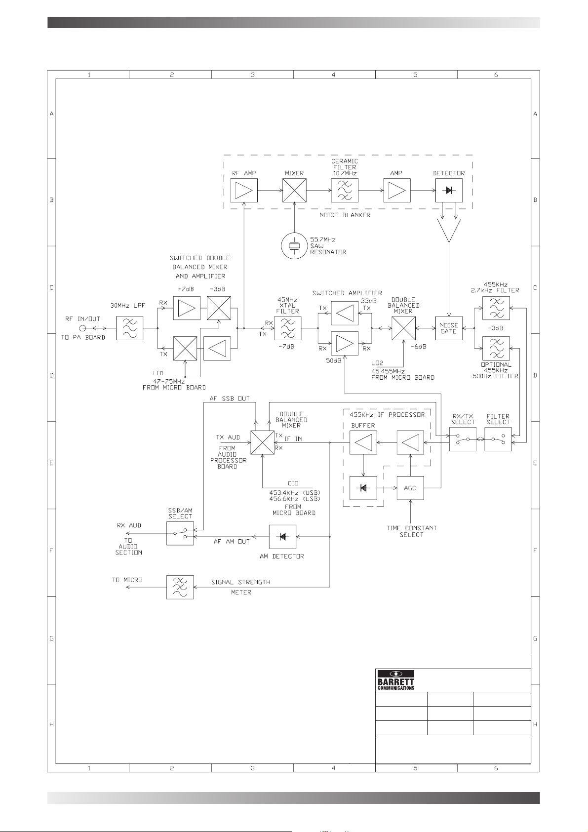
The RF section of the RF / Audio PCB provides the complete exciter and receiver for the transceiver. It
includes:-
First mixer Roofing filter at 45 MHz
45 MHz IF amplifier with AGC 45 MHz Noise blanker receiver
Second mixer Noise blanker gate
SSB filter and narrow filter forAFSK Envelope detector for AM
Product detector for SSB,FSK andCW signals AGC detector
The RF section has a common RF input and output port and separate audio input for Tx and output for Rx. A
double superheterodyne system is used, with a first IF of 45MHz and second IF at 455 kHz. Three oscillator
injection frequencies are taken from the synthesiser, LO1 at (Carrier frequency + 45 MHz), LO2 at 45.455
MHz and LO3 or the Carrier Insertion Oscillator at 453.3kHz on USB and 456.6kHz on LSB. There is a
separate 45 MHz receiver to generategating pulses for the noise blanker.
The audio section of the RF/Audio PCB handles the routing of audio signals in the transceiver and
implements audio processing and frequency tailoring. It also handles the extensive I/O with the outside
world such as Auxiliary 600 input and output (950, 980 only), computer Interface (950,980 only), ATU
Interface and external alarm. The audio power amplifiers for both the local and remote head speaker
outputs are also fitted on theRF/Audio PCB.
4.2.1.1 30 MHz Low passfilter, first mixer and45 MHz IF amplifier.
Receive
The 30 MHz low pass filter, L16, L20 and associated capacitors, minimises the image response of the
receiver. It also serves to control LO1 breakthrough on both Rx and Tx. The first mixer U29 and post mixer
amplifier Q1 is switched as a block between receive and transmit by relay RL1. The local oscillator level for
this mixer is +13dBm. The amplifier achieves the best possible broadband termination for the mixer IF port,
important to maintain low intermodulation distortion. The post mixer amplifier then feeds into the noise
blanker receiver via an isolation amplifier Q28, and also into the main receiver IF section via a dual section
45 MHz roofing filter giving medium selectivity of approximately +/- 3 kHz @ -3dB and +/-25 kHz @ 60dB.
The roofing filter feeds or is fed by the dual gate FET 45 MHz IF amplifier consisting of Q4 and Q5. The input
of this IF amplifier is matched to 50 by L1 and C21. The output is matched to 50 by the L network L9, C37.
AGC is applied to the 45MHz IFamplifier via the second gateson Q4and Q5. RL2 and RL3 control theTx/Rx
turn around of this IF amplifier.
Transmit
In transmit the 45MHz IF amplifier is reversed in its direction by relay RL2 and RL3, the output from the
second mixer is amplified by this 45MHz amplifier which in the transmit direction is gain controlled by a
voltage switched in place of the AGC signal. This voltage is adjusted by VR2 which sets the drive of the
exciter. The output of the 45MHz IFamplifier isthen passed through the 45MHz roofing filter consisting of F2
and F2A and into the first mixer U29 and its associated post mixer pad and amplifier. The whole mixer, pad
and amplifier is reversed in the direction used in receive by relay RL1. The output of the mixer is fed into low
pass filter consisting of L16, L20 andassociated capacitors.
PAGE 19
Page 20
BARRETT 900 SERIES TRANSCEIVERS
PAGE 20
SYSTEM BLOCK DIAGRAM
DRAWING NUMBER
900B62A4.PCB
SCALE
NTS
DRAWN
GMH
DRAWING TITLE
DATE
25-1-99
DIMENSIONING
DESIGNED
BARRETT 900 RF AUDIO BOARD
RF SECTION
RAG
/
ECN REFERENCE
BARRETT PART NO
SHEET
1OF1
Page 21

BARRETT 900 SERIES TRANSCEIVERS
4.2.1.2 Second mixer and bandpasscrystal filter.
The 45 MHz signal from the IF is converted to 455 kHz by the second mixer U13 which is a double balanced
ring mixer, and is fed with a +7 dBm oscillator signal at 45.455 MHz from the master oscillator on the
microprocessor PCB. T6 (and T4, if the narrow filter option is fitted) provides the necessary impedance
matching into the second IF ceramic filter F1 (second IF crystal filter F6, if the narrow filter option is fitted).
This filter gives the final selectivity for the system of 2.3 kHz@3dBand4kHz@60dB.(500 Hz @ 3 dB and
1 kHz @ 60 dB ifthe narrow option is fitted)
4.2.1.3 Noise blanker
The noise blanker receiver is fed from the first mixer output via FET Q28 which acts as a buffer and prevents
the noise blanker receiver local oscillator generating intermodulation products in the main receiver. An FM
superheterodyne chip NE615D, U2 is used with wide ceramic filters F4, F5 to detect impulse noise. The
RSSI output on pin 7 produces a DC level which responds rapidly to noise. A comparator U9 with threshold
adjustment employs an integrator and differentiator on input pins 4 and 5 respectively so that noise blanking
occurs only on rapidly changing signalssuch as noise spikes.
4.2.1.4 Noise gate
The noise gate uses RF switch NE630, U12. This is a high speed switch that when enabled allows the
receive signal from the second mixer to pass directly to the 455 kHz filter. When a blanking pulse from the
noise blanker receiver is present the NE630 U12 switches the RF signal containing the noise pulse away
from the mixer thus blanking thenoise pulse from further processing.
4.2.1.5 Second IF, AGC and demodulator
Following the noise blanker RF switch U12, RF switch U8, switches in the narrow or standard filter as
required. Following the filter(s) on receive, atransmission gate U7 routesthe 455 kHz signalinto the 455 kHz
IF amplifier consisting of U4 and transistors Q11 and Q13. U4 is a wide-band amplifier, the output being
applied to the base of Q11. The output in turn is further amplified by Q13 which is tuned to 455 kHz by T8. In
SSB modes the output of the 455 kHz IF amplifier is fed into the double-balanced mixer U6 which is the
product detector for receive, and the balanced modulator for generating the first I.F. on transmit. The double
balanced mixer is fed by the carrier insertion oscillator ,generated on the microprocessor PCB, which has
frequencies as follows 453.3 kHz for USB, 456.6 kHz for LSB, 453.00 kHz for CW and 456.56 kHz when the
500 Hz filter is in use. When receiving AM, the injection oscillator is switched off. The audio output from U6
pin 6 passes through a switch U14:B to the audio section described below. U14:B switches the output of AM
detector Q18 to the audio section, when AM is selected. The IF signal from Q13 is also fed into Q14 and U5
which comprise the AGC voltage generator. Q14rectifies the IF signal tocharge C53.The voltage on C53 is
thus proportional to the level ofthe received signal. This level is amplifiedby U5A to provide the final A G C
voltage for U4. This AGC voltage is also inverted and level shifted by U33:A, and is applied to the two 45
MHz IF amplifiers Q4 and Q5. These devices need to have AGC applied in the opposite sense to that
required by U4. Q13 also feeds the "S" meter rectifier Q10, which sends the DC proportional to signal
strength to the microprocessor board forprocessing and display.
4.2.1.6 Transmitand receive switching
Switching transistors Q8 and Q12 controlthe Tx/Rx relays and the noise blankerpower supply.
4.2.2 Audio section
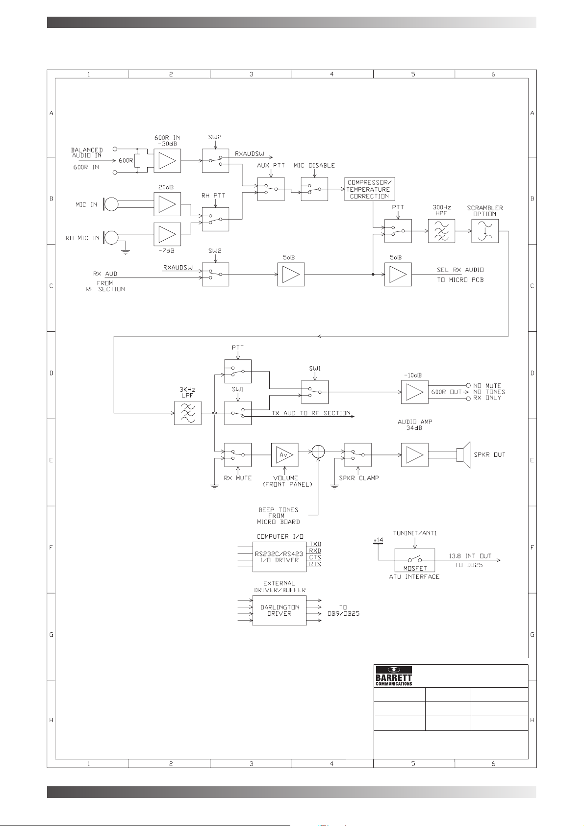
The audio section handles the routing of audio signals in the transceiver and implements audio processing
and frequency tailoring. It also handles the extensive I/O with the outside world such as Auxiliary 600 input
and output (950 only), Computer Interface (950 only), ATU Interface and external alarm. Audio muting and
the Loudspeaker drive amplifier are alsofitted on the PCB.
PAGE 21
Page 22

BARRETT 900 SERIES TRANSCEIVERS
4.2.2.1 Audio path
receive
In the demodulated Rx audio signal at a level of 50 mV P-P is fed into amplifier U22:B which raises
this level by 5dB. This signal is then split and fed to the main signal path and to the microprocessor PCB via
U22:A, where it is used in the mute and selcall system. Bilateral switch U14:C performs Tx/Rx changeover
for the main audio path and the signal then follows a common path through scrambler jumper J1, voltage
follower, U17:A, and 3kHz LPF U17:B. Bilateral switch U21:A is the mute gate which couples the received
audio to the voltage controlled amplifier (the volume control IC) IC's U28 and U32 via buffer U24:B. U27:B is
used to disable the audio tothe 600 balanced audio output portduring transmit i.e. when PTT PA is active.
U27:A and U27:C direct the transmit audio TX AUD to the 600 balanced audio output when SW1 is active.
This is for use when remotecontrol functions are required.
The voltage controlled amplifiers IC's U28 and U32 are controlled by voltages from the volume
potentiometers from the remote head (when fitted) and the front panel (when fitted), respectively. The
receive audio signals from the volume control IC's are then combined with audio beeps and alarms (AUD
ALARM) from the Microprocessor PCB and fed to the speaker clamps Q22 and Q23 repectivley, which
suppress the audio on transmit. The power amplifier U23 raises both the audio signals to 2 W maximum in
order to drive the loudspeaker in either the remote head or front panel (which ever or both of which may be
fitted). Auxiliary muted Rx audio is available via balanced output amplifierU19 delivering 0dBm into 600 .
transmit
In a balanced op-amp U15:B provides 20 dB of mic gain for the local microphone. When the
auxilairy input is in use the auxiliary balanced amplifier U15:A receives signals at 0 dBm (600 ) input. When
the remote head microphone is in use the high level single ended mic audio from the remote head is
buffered by U24:A. The selected Tx audio signal in use at the time passes through the bilateral switches
U11:B, U16:A or U16:B to the Tx audio compressor circuit consisting of U18:B, Q27 and U18:A which
maintains a constant audio output over a large input range. Q27 acts as a variable resistor, controlled by
the output of the rectifier U18:B and D22. C107 is the timing capacitor. R217 controls attack time, and R141
controls release time. Transmit audio temperature compensation is provided by the network consisting of
TH1, R219 and R221. On transmit the signal is routed through the bilateral switch U14:C and on through
the common path of J1 and LPF. Jumper J1 is an ideal point to measure both transmit and receive audio.
The signal then passes directly tothe IF section where it is usedto modulate the exciter.
PAGE 22
Page 23
BARRETT 900 SERIES TRANSCEIVERS
SYSTEM BLOCK DIAGRAM
DRAWING NUMBER
900B63A4.PCB
SCALE
NTS
DRAWN
GMH
DRAWING TITLE
DATE
16-2-99
DIMENSIONING
DESIGNED
BARRETT 900 RF AUDIO BOARD
AUDIO SECTION
RAG
/
ECN REFERENCE
BARRETT PART NO
SHEET
1OF1
PAGE 23
Page 24

BARRETT 900 SERIES TRANSCEIVERS
4.3 PA PCB
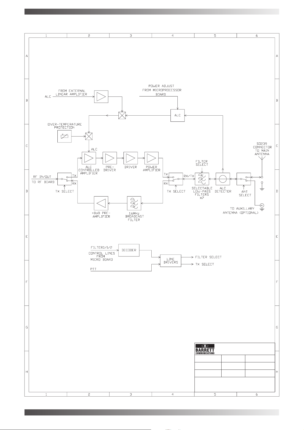
The Power Amplifier raises the power from the exciter to specified output power. It also provides harmonic
filtering for the transmitter, andband filteringand a 8 dB RF pre-ampfor the receiver.
4.3.1 Gain control amp
The signal from the exciter at a level of approx. 35 mV P-P is fed to a gain controlled amplifier U1. This stage
gives a gain variation of 13 dB. Transistor Q1 is configured as an emitter follower to provide buffering, gain
stage Q2 raises the signal level suitable to drive the first of two push pull power amplifiers. This pre-driver
stage employs RF negative feedback viaT1, R12 and C4 to achieve lowdistortion.
A push-pull drive stage Q3 and Q4 is employed to raise the power to a level suitable to drive the 100 W - 125
W power amplifier stage. Transistor Q19 provides the bias reference for the driver stage. Final amplification
to the output level is achieved using Q5 and Q6 in push-pull. This final amplifier stage has an active bias
circuit using U4:A and Q7 with Q21 providing a bias reference which thermally tracks the power devices due
to physical contact.
4.3.2 Low pass filters
Sub-octave harmonic filtering is provided by seven Cauer-Chebyshev filters with bands of 1.6 to 2.48 MHz,
2.48 to 3.84 MHz, 3.84 to 6.0 MHz, 6.0 to 9.3 MHz, 9.3 to 14.5 MHz, 14.5 to 22.48 MHz and 22.48 to 30.0
MHz. These are selected bya3to8decoder U9 which drives a Darlington driver U8 to select the relevant
LPF relays.
4.3.3 ALC control
Forward and reverse power sampling for the ALC system is implemented using current transformer T4 and
detector diodes D5 and D4. A dual time constant system is used in the ALC detector which feeds the main
ALC amplifier U3. This amplifier compares the incoming combination of forward and reverse power with a
reference voltage and generates a control voltage which is fed through the emitter follower buffer Q12 to the
gain controlled amplifier. Both forward and reverse power DC levels are buffered by U7 and fed to the Micro
PCB. When optional external linear amplifiers are used ,U3B buffers an external current sourced ALC signal
from these linear amplifiers to control the power output of the PA. Output power is preset by a DC
voltage generated by the microprocessor PCB and fed to the ALC circuit via pin 19 of the 26 way connector
P2.
4.3.4 Over-voltage and reverse voltage protection
Overvoltage and reverse voltage protection is incorporated on the PA PCB (Q10, Q11, D2, D14 and SCR1)
and transorb. diode D3 absorbs anyinstantaneous voltage peaks over 18 volt.
4.3.5 Auxiliary antenna socket
A switching system on the PA PCB, configured using J2, enables an optional UHF connector to be fitted on
the rear of the transceiver. Once fitted the two UHF connectors are configured as described in section 7 of
this manual. The second antenna socket position in the chassis can also be used to locate the GPS BNC
antenna socket when the internal GPSreceiver option is fitted.
4.3.6 Receiver RF amplifier
The receive RF pre-amplifier consisting of Q22, T5 and associated components provide 8 dB gain at the
front end of the receiver. This amplifier is preceded by a high pass filter L12, L13, and associated capacitors
to prevent strong broadcast band transmissionsfrom interfering with the wanted signal.
4.3.7 Power supply regulators
Regulator U5 provides the +10 V power rail for use in all sections of the transceiver. Q8 switches the +10 V
power rail to provide +10TX on the PA during transmit mode. U2 provides the +5 V rail, again used in many
sections of the transceiver. Q16 switches the +5 V power rail to provide 5VTX used on the PA during transmit
mode
PAGE 24
Page 25
BARRETT 900 SERIES TRANSCEIVERS
SYSTEM BLOCK DIAGRAM
DRAWING NUMBER
900B57A3.PCB
SCALE
NTS
DRAWN
GMH
DRAWING TITLE
BARRETT 900 PA BOARD
DATE
16-2-99
DIMENSIONING
DESIGNED
TRB
ECN REFERENCE
BARRETT PART NO
9603
SHEET
1OF1
PAGE 25
Page 26

BARRETT 900 SERIES TRANSCEIVERS
4.4 Front panel
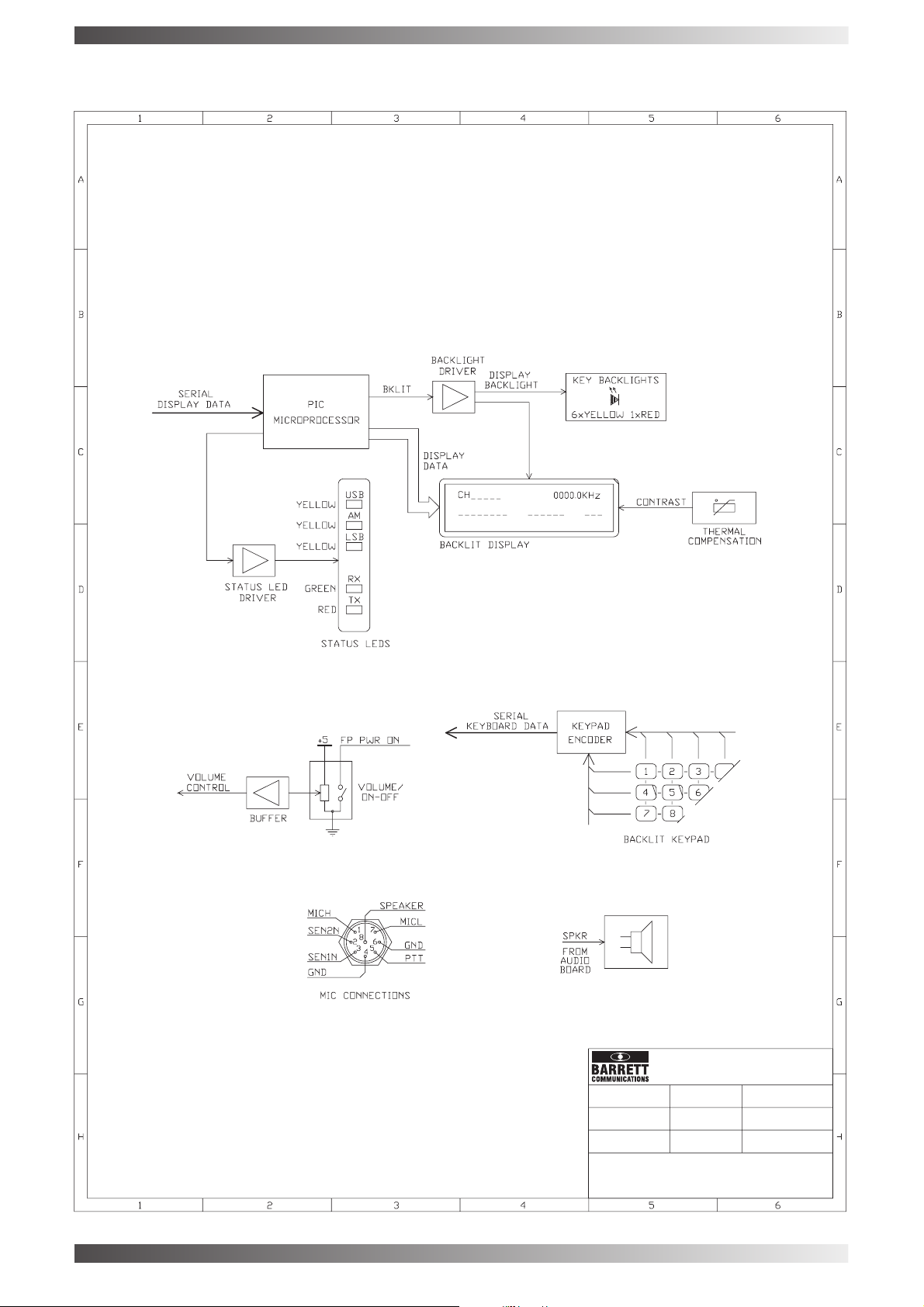
The Front Panel PCB allows user control of the transceiver. An integral rubber keypad provides functional
control. The LCD display presents channel, frequency and status information and the five status LED's
indicate mode and Tx / Rx state. Backlighting for the LCD and keys is provided and a volume control varies
the audio level from the loudspeaker. A microphone socket allows the use of a three button microphone,
providing PTT and channel Up/Down functions. Note:- The standard microphone has a jumper in it (refer to
the microphone diagrams) that enables the front panel speaker, the handset does not have this jumper thus
disabling the speaker.
4.4.1 LCD and status LED's
Data to refresh the front panel LCDis sentfrom the microprocessor PCB,via theAudio / IF PCBon one serial
data line. This serial datais processedon thefront panelby embeddedmicroprocessor U1,and convertedto
parallel data for use by the LCD and mode and operational state status display LED's. Q8 provides buffering
of the serial data line fromthe main body of the transceiver.
4.4.2 Keypad
Data from the 20 function keypad matrix is PWM encoded by the keyboard encoder U2. This is buffered by
Q9, and sent via the control cable and the RF/Audio PCB to the microprocessor PCB. The microphone
channel up and down buttons are also handled by U2. Channel up and channel down functions come from
the microphone socket pins 3 and2 respectively.
4.4.3 Backlighting
Backlighting for the keys is provided by parallel LED's D6-D12 which are in series with the LCD display's
internal backlight diodes. Port RB7 and RB6 are used to provide intensity control of the LCD via Q1.
Extended temperature range on the LCD display is achieved by controlling the polarising voltage on pin 3
using a thermistor TH1.
4.4.4 Microphone
The microphone socket has EMC filters to prevent pick up of RF by the balanced microphone leads. Two
lines allow the channel up/down keyfunction on the microphone as described above.
4.4.5 Volume control andOn/Off switch
The volume control VR1 provides a voltage that controls the voltage controlled amplifier located on the
RF/Audio PCB The lower the voltage output from VR1's wiper the higher the volume. The On / Off switch
provides a ground to the main body of the transceiver to switch the transceiver on. This ground is also used
to apply the 13.8 VDC tothe front panel, this in turn switchingon the +5V DC supply for thefront panel logic.
.
PAGE 26
Page 27
BARRETT 900 SERIES TRANSCEIVERS
SYSTEM BLOCK DIAGRAM
DRAWING NUMBER
900B59A1.PCB
SCALE
NTS
DRAWN
GMH
DRAWING TITLE
BARRETT 900 FRONT PANEL
DATE
24-12-97
DIMENSIONING
DESIGNED
PHW
ECN REFERENCE
BARRETT PART NO
SHEET
1OF1
PAGE 27
Page 28

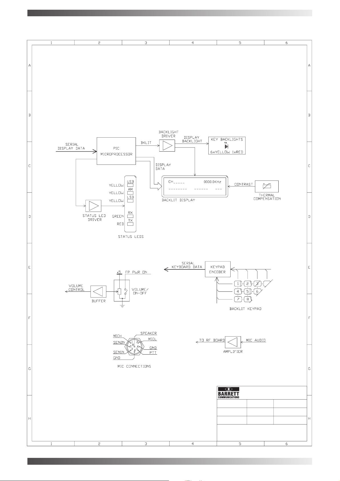
4.5 Remote control head
The on/off switch on the volume control potentiometer completes the circuit to ground and activates the
power relay on the PA in the transceiver's main body through the remotecontrol cable via line RH PWR SW.
In addition the on/off switch turns on Q6 allowing +14 V power feed to the regulators U7 and U6. The 5 V
regulator U6 supplies the digital ICs and the second 5 V regulator U7 is stacked on the first to obtain 10 V for
the analogue circuit.
Keyboard encoding is handled by U2, a matrix encoder chip that provides a PWM coded output only when a
key is depressed. The microphone up and down buttons are also handled by U2.The serial output from U2 is
buffered by FET Q8 and emerges at connector P1 as RH SKB OUT for eventual decoding by the
microprocessor.
Serial data from the transceiver's main body is sent to the remote head on line RH SD INB via the remote
head interface cable. This serially coded data is decoded by embedded microprocessor U1 and distributed
in parallel form to either the LCD or mode and status LED's as required. LCD contrast is temperature
compensated by thermistor TH1. Q1 switches the LCD and keypad back-lighting on and off by computer
control.
BARRETT 900 SERIES TRANSCEIVERS
PAGE 28
Page 29
BARRETT 900 SERIES TRANSCEIVERS
SYSTEM BLOCK DIAGRAM
DRAWING NUMBER
900B60A1.PCB
SCALE
NTS
DRAWN
GMH
DRAWING TITLE
DATE
DIMENSIONING
DESIGNED
BARRETT 900 REMOTE HEAD
24-12-97
PHW
ECN REFERENCE
BARRETT PART NO
SHEET
1OF1
PAGE 29
Page 30

5.0 Maintenance
5.1 Introduction
This section provides maintenance and fault finding procedures that can be carried out on Barrett 900 series
transceivers.
5.2 Printed Circuit Board (PCB) maintenance
Barrett 900 series transceivers use four layer PCB's for the microprocessor and RF/Audio sections and two
layer PCB's, for the PA , front panel and remote head. When working on these PCB's observe the following
precautions:-
Excessive heat could lift a track from the circuit boards, resulting in serious damage. Avoid the use of highpowered soldering irons. A soldering iron rated at a maximum of 60W and temperature controlled to
approximately 370 C is suitable for most tasks. For removal or installation of heavier components such as
PA transistors and main power leads a soldering iron rated at a higher temperature of 425 C is required.
When unsoldering, use a solder-sucker orSolder wick to remove the solder.
Burned or broken sections of printed circuit track may be repaired by bridging the damaged section with
tinned copper wire. Care must be taken to remove the PCB solder mask covering the track either side of the
burn or break to allow it to be tinned before making the repair. Also in the case of a burn, the fibreglass area
that has been burnt must becleaned to remove any carbon deposits.
BARRETT 900 SERIES TRANSCEIVERS
5.3 Component replacement
When replacing defective diodes, transistors, electrolytic capacitors or integrated circuits, observe any
marking that indicate polarity or orientation. It is essential that these types of components are installed
correctly.
Components with leads that are soldered into plated through holes in the PCB such as integrated circuits,
diodes, resistors andcapacitors, can often be replaced with the minimum of risk byclipping its leads as close
to the component as possible. The leads left in the PCB can then be removed by carefully heating the solder
joint on each remaining lead individually, then carefully withdrawing the lead from the PCB using a pair of
pliers. Avoid pulling on the lead before the solder has fully melted around the lead as damage to plated
through holes or layers of the PCB may occur. Once the component has been removed use solder wick or a
solder sucker to clear the remainingsolder from the hole.
When replacing heat sensitive components to the circuit board, if possible use long-nosed pliers or similar to
conduct heat away from the component.
When replacing PA output transistors and drivers ensure that the thermal conduction paste between the
heatsink and the component is replaced. This can be achieved by cleaning the mounting surfaces, and recoating them with a thermal conduction compound. Only use a small amount of thermal compound but
enough to make a light coveron the surface.
Extensive use of surface mounted components is made on all PCB's in 900 series transceivers. It is
essential that surface mount work stationsbe used for removal and replacement ofthese components.
Note that there are some capacitors on the Microprocessor board which require special low temperature
solder and soldering equipment. These capacitors can be recognized by their silvery appearance. They are
C8, C9, C34, C35, C194, C173.
PAGE 30
Page 31

BARRETT 900 SERIES TRANSCEIVERS
5.4 CMOS devices
A number of Complementary Metal Oxide Semiconductor (CMOS) devices are used in the transceiver and
most of them have built-in protection. However, their extremely high open-circuit impedance makes them
susceptible to damage from static charges. Care must be used when handling these devices during
servicing. By observing the following precautions,the risk of damage to CMOS deviceswill be minimised:-
Replacement CMOS devices are supplied in special conductive packaging. They should remain in this
packaging until required for use.
Ensure that power supplies are switched off before making connection or disconnections between circuit
boards.
Handle circuit boards and touch conductiveparts as little as possible.
Anything connected to or touching thecircuit board tracks should be grounded.
Make sure test equipment being usedhas a correct earth on its mainslead.
Before and during work on PCB's or handling CMOS devices, discharge static charges, which may build up
on a person, by touching a grounded metal surface with both hands. If possible wear a suitably grounded
conductive wrist strap.
5.5 Transmitterpower amplifier maintenance precautions
When making measurements of the low level stages of the exciter, it is advisable to remove the drive to the
PA and Filter PCB, this can be achieved by removing the coaxial cable from the RF/Audio PCB to the PA
PCB by carefully unsoldering it. If working on the whole system with the power amplifier connected, caution
should be exercised when connecting probes in the area of the MC1350 gain controlled amplifier as a probe
can cause instability which can drive the power amplifier to full power without ALC action being available
resulting in damage to the power amplifier. When connecting probes to the PA assembly, the earth clip lead
should be wound around the bodyof the probe and the earth clipshould be connected to the ground plane,
adjacent to the point of measurement to which the probe tip is connected, thus reducing any stray RF pickup.
5.6 PCB access
5.6.1 930 - 950 - 980 transceivers
Removing the top cover gives accessto the microprocessor PCB.
Removing the bottom covers gives access to the RF/Audio PCB and PA PCB. The RF/Audio PCB is
mounted under a separate RF shieldplate held in place with two screwsand a slot behind the front panel.
5.6.2 940 transceivers
Referring to figure 940 chassis explosion diagram remove the battery pack from the transceiver, remove the
six hex head screws from the rear of the transceiver, carefully remove the back plate to the extent the power
cable will enable then rotate and slide the aluminum extruded cover by sliding it upwards, allowing the back
plate to pass through the centreof the cover extrusion.
5.6.3 930 - 950 remote control head
Remove the two screws on the rear panel of the remote control headallowing the front panel and rear shell to
be separated.
PAGE 31
Page 32

BARRETT 900 SERIES TRANSCEIVERS
5.7 Fault diagnosis
5.7.1 General
The circuit diagrams show both DC and signal voltage points to enable a faulty section to be located. It
should be noted that given voltages are typical and allowance should be made for variations between
transceivers. The following diagnostic sequences are general guides only. The use of normal trouble
shooting principles and reference to the technical description, circuit diagrams and overlays will be
required when diagnosing faults.
The removal andsubstitution ofcomponents maydamage thecomponents and/or the printed circuit boards.
In some cases, it is impossible to remove components without destroying them. It is important therefore to
carry out as much diagnosis as possible without removing components. The following general points should
also be of assistance:
Replacement boards spare boards
substituted to localise the fault toone board.
Transistor tests - static
collector junctions, or a short circuitbetween emitter and collector.
These types of faults can usually be detected without removing the transistor, using the ohms range of an
analogue multimeter or diode test ona digital multimeter.
The two junctions should both give the appearance of a diode, that is high resistance with the multimeter
leads one way round and low resistance when the leads are reversed. Polarity depends on whether a PNP
or NPN transistor is being tested. The resistance between collector and emitter should be high with the
multimeter leads either way round. The circuit diagram should be examined for parallel paths across these
junctions caused by low resistance devices such as inductors before you remove a transistor that fails these
tests.
Transistor tests - dynamic,
circuit. One of the most significant voltage measurements is the base-emitter voltage. The polarity of this
will depend on the type of the transistor (PNP or NPN). A base emitter voltage of between 0.6V and 0.8V
should be measured on a forward-biased base-emitter junction. 1.2V to 1.6V for a Darlington transistor.
With its base emitter junction forward-biased the transistor should conduct. Some indication of satisfactory
operation of the transistor can be obtained by measuring the voltage drop across its collector or emitter
resistor and short circuiting its base to the emitter. The short circuit removes the forward bias cutting off the
transistor,so that the voltage across the resistor is considerablyreduced.
Integrated circuits
should be ascertainedwhether thefailure isdue tothe ICitself orthe loadit isdriving into. As a general rule, if
changes in the input cause absolutely no changes in the corresponding output, the IC should be suspected.
If however, a very smallchange in output can be detected, the load ismore likely to be the cause. Depending
upon the circuit, make further tests by disconnecting resistors, capacitors, etc to verify the diagnosis before
removing the IC.
, transistor failures are most often due to open - circuit base- emitter or base
some transistor faults can be diagnosed by measuring voltages within the
, if thereappears to be no output from an integrated circuit, before replacing the device, it
- if replacement spare boards are held in stock, they may be
If a fault can be traced to one PCB but no further then consider using Barrett Communications' PCB and
module exchange service.
PAGE 32
Page 33

BARRETT 900 SERIES TRANSCEIVERS
5.7.2 Transceiverwill not power up
Plug the transceiver into a 13.8 VDC power supply, switch the transceiver on, if the transceiver is totally
inactive:-
- Check voltageon the input power cable on the PAPCB is between 11.8 VDC and 14.5 VDC.
- If using a remote control head, check the cable between the head and the main body of the
transceiver
- Check the26 way cable between the PA and the RF/Audio PCB's.
- Check the14 way cable between the Front Paneland the RF/Audio PCB's.
- Check the 50 way connectors are mated between the RF/Audio and the microprocessor
PCB.
- Check the Cathode of D1 on the PA PCB is > 10 V when the transceiver is off and low when it
is switched on.
- If a single relay click is audible on switch on butthe transceiveris otherwise inactive the 3.15A
fuse on the PA PCB is probably blown. Check for obvious damage or short circuits prior to
replacement.
- Check allthe voltages as indicated in the tablenext page.
PAGE 33
Page 34

Voltage table
Location Drawing No. Supply Test Voltage Voltage Source PCB
PA 900S18##.PCB 14 TP7 +13.8 V +13.8 V external
PA 900S18##.PCB +10 - +10V +/- +10V +/- PA - U5
PA 900S18##.PCB +5 - +5V +/- +5V +/- PA - U2
PA 900S18##.PCB +5TX - 0V +5V +/- 0.2V PA Q16
PA 900S18##.PCB +10TX - 0V +10V +/- 0.2V PA - Q8
PA 900S18##.PCB +12TX - 0V +12V nominal PA - Q9
BARRETT 900 SERIES TRANSCEIVERS
rail point Receive Transmit and
name regulator or
transistor
nominal nominal source
0.2V 0.2V
0.2V 0.2V
RF/Audio 900S15##.PCB +14 - +13.8 V +13.8 V PA - external
900S27##.PCB nominal nominal source
RF/Audio 900S15##.PCB +10 - +10V +/- +10V +/- PA - U5
900S27##.PCB 0.2V 0.2V
RF/Audio 900S15##.PCB +5 - +5V +/- +5V +/- PA - U2
900S27##.PCB 0.2V 0.2V
RF/Audio 900S15##.PCB BIAS TP12 +5V +/- +5V +/- RF/Audio - U5:B
900S27##.PCB 0.2V 0.2V
Micro. 900S14##.PCB +14 - +13.8 V +13.8 V PA -external
nominal nominal source
Micro. 900S14##.PCB +10 - +10V +/- +10V +/- PA - U5
0.2V 0.2V
Micro. 900S14##.PCB +5 TP14 +5V +/- +5V +/- PA - U2
0.2V 0.2V
Micro. 900S14##.PCB +5D TP4 +5V +/- +5V +/- Micro - U19*
0.2V 0.2V
Micro. 900S14##.PCB +5VA TP3 +5V +/- +5V +/- Micro -U20*
0.2V 0.2V
Fr. Panel 900S16##.PCB +14 - +13.8 V +13.8 V PA - via RF/Audio
nominal nominal
Fr. Panel 900S16##.PCB +5 - +5V +/- +5V +/- Fr. Panel - Q6
0.2V 0.2V
Rem. Head 900S17##.PCB +14 - +13.8 V +13.8 V PA - via
nominal nominal RF/Audio
Rem. Head 900S17##.PCB +10 - +10V +/- +10V +/- Rem. Head - U7
0.2V 0.2V
Rem. Head 900S17##.PCB +5 - +5V +/- +5V +/- Rem. Head -U6
0.2V 0.2V
Note :- ## denotes the rev number, this may change
PAGE 34
Page 35

BARRETT 900 SERIES TRANSCEIVERS
5.7.3 Transceiverwill not receive but displays OK
It is assumed in this sectionthat, the transceiver turns on and displaysare normal.
5.7.3.1 No receiver noise atall
-
- Check thatthe audio mute, selcall mute or signalstrength mute is switched off
- Check theaudio path from the product detector
- Ensure jumperJ1 on the RF/Audio PCB is inplace, no receiver audio will be heardif it is not.
- With the volume control at full and mute off, and USB mode selected, inject a reasonably high level
5.7.3.2 Receive noise present, butdoes notreceive
- The nextsteps assume audio injection can be heardback to TP17, as in section 5.7.3.3.
- Set modeto upper or lower sideband.
- Check that the carrier injection oscillator is present on the coax from the microprocessor PCB going
- Check the second local oscillator LO2 is present on pin 2 of the second mixer U13. It should have
If using a remote control headcheck the speaker is plugged in.
audio signal starting at TP17, on the output of the product detector, and progress up the audio chain
via J1, TP24, TP21 in the case of the local control front panel and TP13 in the case of the remote
control head, eliminating sections of the audio path as you go. If the audio signal could be heard at
TP17 then the fault lies further back in the receiver and you should proceed to the section 5.7.3.2 "Receiver noise present but no receive".
to U6 pin 8 via C74 and R71. It should have a frequency of approx. 453kHz and a level of 1V P-P. If
not present or correct go tosection 5.7.3.6 - VCO faults.
a frequency of 45.455MHz and a level of approx.1.4V P-P (+7dBm). If not present or correct go to
section 5.7.6 - VCO faults.
- Check the first local oscillator LO1, generated by a phase locked loop on the microprocessor
PCB, is "locked", indicated by the red LED on the microprocessor PCB being extinguished (off).
Then with a channel frequency programmed to 2.000 MHz the frequency if the LO1 should be
47.455MHz (SCF + 45.455MHz) with a level of approx 2.8V P-P (+13dBm). If the VCO is unlocked
or the LO1 is not presentor correct go to section 5.7.6 -VCO faults.
- Check the receiver AGC voltage on TP31 is 3.8V under no signal condition. If not investigate
the AGC generator and allsupply voltages in the area.
- Now inject signals of correct frequency and levels as per the tables on the relevant RF/Audio PCB
schematics moving back up the receiver path towards the antenna progressively eliminating check
points and eventually locating the faultysection.
5.7.3.4 Transceiverturns on but displays "Barrett 900 Transceiver" only
- On power on the front panel LCD display or remote head LCD display will initially show a
banner "Barrett 900 Transceiver" and the RX and AM LEDs will be lit. This is generated, as a
power on message, by the front panel and remote head micro, before the main microprocessor in
the transceiver starts communicating with it. When the main microprocessor communicates with the
front panel or remote head the display will change to the current channel and the LED's will indicate
the channel mode.
- If the front panel or remote head remains displaying only the banner "Barrett 900 transceiver, and
does not progress to the channel information, either the main microprocessor is inactive, in which
case refer to the section on main microprocessor faults, or the path carrying the serial data from the
microprocessor to the front panel is faulty. The serial signal that updates the front panel and remote
head displays is SD out. On the RF/Audio PCB this becomes SER DISP. SER DISP is split into two
signals by two inverters U25 D and U25 E becoming FP SD for the front panel and RH SD for the
remote head.
.
PAGE 35
Page 36

BARRETT 900 SERIES TRANSCEIVERS
5.7.4 Transceiverturns on, internal voltages are normal, butno LCDdisplay.
- In the case of the remote control head check the remote control head microprocessor for
activity or an LCD module fault.
- In the case of the front panel check the front panel microprocessor for activity or an LCD module
fault.
5.7.5 Main microprocessor faults
- Check that the transceiver firmware EPROM U4 and option GAL U30 are fitted, without these the
transceiver will not operate.
- Observe the LED's on the Microprocessor PCB. Check that all the yellow LED's are illuminated at
the same intensity. The LED's check the +5V, +5V DIGITAL,+5V ANALOG and +10V rails. If any of
these LED's are extinguished there is a problem on the corresponding rail and the rail should be
checked for shorting to ground.
- Check for a 2.7MHz logic level square wave at pin 1 of U13 74HC4040 on Microprocessor PCB. If
the 2.7MHz is present, then the reference oscillator is active, otherwise there is a fault in the
reference oscillator chain. A fault in the reference oscillator chain can be localised by
examining microprocessor PCB test points TP31, TP30, TP33 and TP32 in turn. By comparing the
waveforms obtained, with those on the schematic diagram table it should be possible to isolate
the problem.
- If with the standard reference oscillator fitted the crystal oscillator comprising Q13, Q14, L15,
L16, X3 etc is not running, then check that the crystal oven is hot and that the DC levels are
appropriate.
- If the high stability reference oscillator is fitted check for output. If no output is present check the
DC level into the TCXO/DCXO is correct. If it is and no output is evident then replace the
TCXO/DCXO. Incorrect DC levels generally indicate a failed transistor. As Q13 and Q14 are not
DC coupled the faulty device shouldbe obvious.
- If the reference chain is working up to pin 1 of U13 then check for 22.7MHz logic clock at TP34
and 11.3MHz logic clocks at pin 33 of the microprocessor U1. Absence of clocks at either point
indicates a problem with U31, 74AC74or U32, 741C74.
- If both clocks are present the next step is to check address latch enable at TP6 as in the table on
the schematic, and then check for microprocessor bus activity. This can be monitored on a CRO,
and it should be possible to see continuous bus activity on the address and data pins of the
EPROM.
- If no bus activity is evident check that TP38, the reset line is high and that the stop line, pin 68 of
U1, is also high. Also check thatTP5 the interrupt line is normally highwith brief pulses low.
-
Erratic bus activity with no sensible display on the LCD indicates a possible bus problem. The
only way in which this can readily be isolated apart from checking for bus shorts, with a
multimeter, is by fitting a CHECK EPROM Barrett P/N BCS90100 which has been programmed
entirely with OOH data at each address. With such an EPROM fitted the microprocessor will
simply step through each address without stopping or jumping and the waveform on each
address bit from A0 to A14 on the EPROM should be a square wave at successively half the
frequency for each successive bit.
- Normal accessing of EPROM and EEPROM can be checked by comparing the waveforms
obtained at TP6 and TP1 againstthose in the schematic table.
PAGE 36
Page 37

BARRETT 900 SERIES TRANSCEIVERS
5.7.6 VCO faults
- If the transceiver beeps satisfactorily, the status LED's are correct and receiver noise is present but
the display indicates HARDWARE FAILURE VCO LOCK LOST, then there is a problem with the
frequency synthesiser. The red LED on the microprocessor should be illuminated under these
circumstances. Select a channel inthe range 8 - 20MHz.
- To localise the PLL failure carry out the following checks: Check for square wave at TP22. If this is
present then the DDFS, DAC, LPF and buffer can be assumed to be operating. If there is no square
wave then work back through TP21 and TP20 with reference to the schematic waveforms until the
problem is located. Absence of a sine wave atTP21 probably indicates a DAC or QUALCOMM chip
fault. The DACs U8 andU9 have very short pins and shouldbe checked for connection faults.
- Next check for a square wave at TP28. If this is present then the VCO, LPF, buffer and ÷10 pre-
scaler are probably functioning. If no square wave is present then check TP39. This should be
high, otherwise the pre-scalar is held in reset. Check for large swing of RF at pin 8 of U21:C. If this
is not present then check TP36to ensure that 3V P-P RF isbeing generated by the VCO.
- If square waves are evident at TP22 and TP28 and the PLL is not in lock then the square waves will
be at different frequencies. Check the DC level at TP26. If this level is low (0V) then there is
possibly a fault with the charge pump transistors Q4, Q5 BFT92 whereas if the level is high (10V)
then Q2, Q3 BFR92 should bechecked.
- When the VCO is in lock and the red LED is extinguished and the channel frequency is above 8MHz
then the two green LED's onthe Microprocessor PCB should be illuminated. These indicatethat the
VCO is delivering the correct RFlevel.
5.7.7 Transmitterfaulty
If the transceiver will not transmit, it is first necessary to determine which of the modules is at fault.
First disconnect the coaxial cable between the RF/Audio PCB output and the PA PCB input. Do this
at the RF/audio PCB end. Connect a coaxial cable from the RF/Audio PCB output to an
oscilloscope. Terminate the oscilloscope input in 50 ohms. Set the transceiver frequency to 10 MHz.
Either inject a two-tone test signal into the mic socket or whistle into the mic with the PTT activated.
A signal of approx. 35 mVP-P should be observed. If this signal is absent orvery lowthen the fault is
likely to lie in the RF/AudioPCB, if not, re-connect the cable betweenthe two PCBs.
Now check the two fuse links LK1 and LK2 on the PA. If either have blown, then investigate the
possibility of driver or PA transistor failure before reconnecting the power. If it is not these transistors
then a relay fault could exist in the output filter circuit this causing high collector current in the PA
transistors, due to the ALC being disabled in this condition, and as a result of the load mismatch
caused by the faulty relays.
If the fuse links are intact, measure the bias voltage at the bases of the driver and PA transistors with
PTT activated but with notwo toneor speechinput. The voltage should be between 0.5V and 0.7V. If
correct then check the DC voltage on the driver and PA collectors. These should be between 12V
and 14V. If these voltages are within limits, then it is likely that the driver or PA transistors are faulty.
Again inject a two tone signal or whistle into the microphone with the PTT activated and observe the
RF voltage on the driver transistor collectors (Q3, Q4). The swing should be at least 3V P-P. If
correct then the fault is likely to be in the final power amplifier stage. If no voltage swing was
observed on the driver collectors then check the driver base voltage swing, this should be
approximately 1V P-P using a two tone input or a whistle into the microphone. If this is not correct
then the fault could be thedriver transistors, or in U1, Q1, orQ2.
PAGE 37
Page 38

BARRETT 900 SERIES TRANSCEIVERS
5.7.8 Replacement of PA output and drivertransistors
Under normal operating conditions PA and Driver transistors will last indefinitely. The ALC circuit will fully
protect these transistors from incorrect antennaloads.
In data mode, if the cooling fan fails for any reason, a high temperature power reducing circuit will protect
these devices from overheating.
Damage to power transistors is rare and the reasons for failure should be properly investigated if a failed
transistor is found. Reasons for failure include lightning damage, power supply surges, and incorrect
adjustment of bias and power controlcircuits by users.
The driver transistors are either Philipstype BLV11or MotorolaMRF433.
The PA transistors areMotorola type MRF455.
The procedure for replacement of driver and PA transistors is identical, so only the replacement of PA
transistors will be described in detail:
- Disconnect 12V power feed atrear of transceiver.
-
- Prior to removing the PA transistors, the base emitter and base collector junctions should be
checked for forward conduction and reverse leakage using a test meter. In order to do this, the
base leads must be desoldered using a large tipped iron preferably with a No. 8 (800 F) tip. The tab
is bent up to facilitate removal. The tab should be prized up clear of the PCB taking care not to
damage the transistor package. Forward and reversejunction resistance's can then be checked.
- Carefully remove all four M3 crosshead screws which hold the PA transistors in place. Store
them safely.
- Desolder thelarge 100R resistors and 10nF greencaps acrossthe MRF455's.
- Desolder all the solder lugs connecting the flange to ground. Keep these safely. There should be
4 for a pair of transistors. Remove 2 spring washers from under the soldertags.
- Desolder the leads of the BD139 transistor which sits on top of the power transistor flange.
Remove this transistor for later use.
- Prize up the collector leads carefully until they are clear of the PCB. The collectors have a
bevelled tab.
- Prize up both opposed emitter tabs carefully. Extra heat is required here as they are connected to
the ground plane. Remove the transistorsthrough the PCB access hole.
- Remove excess solder from the four PCB pads and clean them with isopropyl alcohol or
methylated spirits.
- Clean all traces of heatsink compound from chassis heatsink area under the transistor being
changed. Ensure that no dirt,swarf or other foreign matter is locatedwhere the transistors will sit.
- Clean the thermal contact surface of the replacement device. Smear a thin layer of heatsink
compound evenly onto the transistor seat. Push the transistor into place and "wriggle" it in-situ.
Remove the transistor and inspect the heatsink area to check that heatsink compound has
coated the seating area of the transistor. A thin but complete smear of compound should be
present. Do not apply too muchor two little as poor thermal conductivitywill result.
- Seat replacement PA transistors carefully in place having bent up collector and base tabs 3mm
from their ends. The bevelledcollector tab should face the large PA transformer.
- Position BD139transistor with metal face down on PA transistor flange.
PAGE 38
Page 39

BARRETT 900 SERIES TRANSCEIVERS
- Place soldertags and spring washers back in positionand fit all four screws in place.
- Go around all four screws in turn, gradually increasing torque until the transistors are firmly
seated.
- Solder the BD139 leads.
- Readjust bias before use.
PAGE 39
Page 40

BARRETT 900 SERIES TRANSCEIVERS
5.8 Adjustments
Following PCB repair, it may be necessary to realign or recheck adjustable components on the relevant
PCBs.
This section describes the methods employed to ensure that the reinstated PCB's conform to the original
specification.
5.8.1 Front panel
There are no adjustments on the front panel. If the LCD display is damaged or a key is non functional the
front panel should be replaced as a complete assembly by removing the two retaining screws and
unplugging the 14 way IDC connector. Should the ON/OFF, volume potentiometer sustain damage, this
is easily replaced by unsoldering the connections to the PCB and undoing the knob collet and retaining
nut.
5.8.2 Microprocessor PCB
There are a number of adjustable components on this PCB which under normal circumstances should be
left untouched.
5.8.2.1 Reference oscillator setup
The 45.455MHz reference oscillator is the internal frequency standard for the transceiver. It must be
adjusted to within a few cycles of declared frequency for reliable operation. It has a PTC thermistor
heating element which stabilises the reference crystal. Before making any adjustment the transceiver
should be left switched on for 5 minutes to allow thermal stabilisation. The core of L16 should be flush with
the top of thecan.
A frequency counter should be connected to TP34 using an oscilloscope, probe set to 10M . Then using a
non metallic trimming tool, L15 shouldbe carefully adjusted to obtain a frequencyof 22.72750MHz Hz.
5.8.2.2 Reference oscillator setup
The 45.455MHz reference oscillator is the internal frequency standard for the transceiver. The high
stability oscillator option replaces the standard oscillator components described above with a modular
45.455 MHz TCXO/DCXO. Unlike the standard oscillator the high stability oscillator can be adjusted
straight after turn on.
A frequency counter should be connected to TP34 using an oscilloscope probe set to 10M . Then using a
trimming tool or small Philips screw driver, the pot in the top of the TCXO/DCXO should be carefully
adjusted to obtain a frequency of22.72750MHz 1Hz.
5.8.2.3 VCO frequency adjustment
Program the transceiver to 30MHz, measure voltage on TP26. Using a non-metallic trimming tool adjust
the core of L8 to 9.5V. In most case's, the core of L8 will not be required. The red out of lock light should be
extinguished.
(Standard oscillator)
+2
(High stability oscillator)
+
5.8.2.4 Carrier Insertion oscillator peaking
Set the transceiver to any USB channel. Monitor TP37 with a CRO probe on sensitivity 0.5 V/div, 0.5
us/div. Adjust T1 for maximum amplitude on the CRO.
5.8.2.5 VCO Low pass filter
If a spectrum analyzer with tracking generator is available, this filter can easily be adjusted by setting the
two notch frequencies of 119 MHz and 178 MHz. Turn the transceiver off for this adjustment. Connect the
tracking generator to TP27 and the spectrum analyzer input to TP36. Adjust L10 for a notch at 178 MHz,
and L11 for anotch at 119 MHz. The filter responseshould be flat to 76 MHz.
This 50 low passfilter hasbeen factoryset to be flat to 75 MHz and . In
an emergency, satisfactory operation can be obtained by setting L10 core flush with the top and L11 core 5
mm inside can.
PAGE 40
W
should not beadjusted inthe field
Page 41
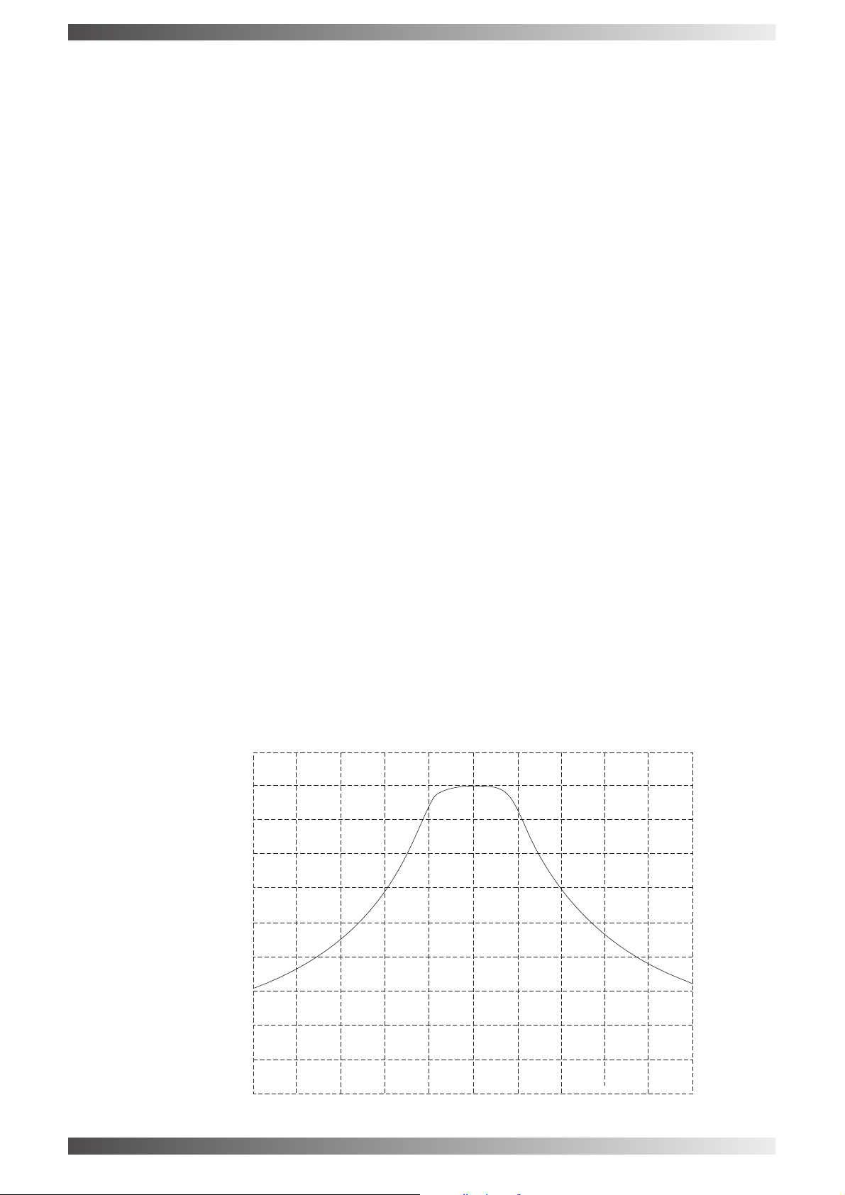
BARRETT 900 SERIES TRANSCEIVERS
5.8.2.6 DAC Low pass filter
If a spectrum analyzer with tracking generator is available, this filter can easily be adjusted by adjusting the
two notch frequencies of 12MHz and 18MHz. The transceiver should be turned off while performing this
adjustment. Connect the tracking generator to TP20, and the spectrum analyzer input to TP21. Adjust L1 for
a notch at 18 MHZ, and L2 for a notch at 12 MHZ. There is no requirement here to check that the filter
response is flat.
This low pass filter has been factory set and . In an emergency,
satisfactory operation can be obtained by setting both L1 and L2, 3mm into the coil can. There are four
yellow LED's which are lit showing correct operation of the +5, +5D, +5A and +10 supply rails. The two
green LED's illuminate above 8MHz dueto local oscillator RF energy.
5.8.3 RF/ Audio PCB
There are 11 adjustable components on the RF/Audio PCB.
and should not beundertaken unlessthe critical components have beenreplaced.
5.8.3.1 Input low pass filter
If a spectrum analyser with tracking generator is available, this filter can be adjusted by adjusting the two
notch frequencies of 69MHz and 47MHz. The transceiver should be turned off for this adjustment. Unsolder
SP3 and connect the tracking generator to TP30, and the spectrum analyzer input to TP14. Adjust L16 for a
notch at 69MHz, and L20 fora notch at 47MHz. The frequency responseshould be flat rom 1MHz to
30MHz
The input low pass filter inductors L16 and L20 should have cores set approximately 5mm inside the cans in
the event of replacement if thecorrect test equipment is not available.
5.8.3.2 45MHz IF Filter
This filter is the most critical filter in the transceiver. Its setting has a direct bearing on the transceiver
dynamic performance. A spectrum analyser with tracking generator must be used to align this filter and it
should be set with a centre frequency of 45MHz and a span of 50kHz. Solder bridge SP1 and SP2 should
be unsoldered, the sweep signal should be injected at TP28 , the spectrum analyser input should be
connected to TP29. L7 and L8should be adjusted to achieve the passband shape asindicated inFig1.1, with
particular attention being given to get the passband asflat as possible. Ifa spectrum analyser is not available
and either L7 or L8 or the crystal filter has to be replaced, rough alignment can be achieved by peaking the
coils for maximum output whilst injecting a weak signal.
this method the filter shape could be incorrect and adjacent channel selectivity, blocking
performance and transmit purity may becompromised.
should not be adjusted in the field
The adjustment of each of these is critical
Note:- Whilst the transceiver will operate using
Fig 1.1
+10dB
0dB
-10dB
-20dB
-30dB
-40dB
-50dB
-60dB
-70dB
-80dB
-90dB
Center: 45 MHz
Span:50 kHz
PAGE 41
Page 42

BARRETT 900 SERIES TRANSCEIVERS
5.8.3.3 IF Inductors
Inductors L5 and L9 can be peaked on a weak signal. As there is a very slight interaction they should be repeaked after initial setting. Leave L1 alone as this is part of the matching network from the crystal filter to the
45 MHz IF amplifier. L1 may be adjusted after the 45 MHz crystal filter has been adjusted as in paragraph
5.8.3.2 by reconnecting SP2, and transferring the spectrum analyzer input to TP4. Set the tracking
generator output level to -60 dBm. Adjust L1 for flattest response. Reverse the spectrum analyzer and
tracking generator connections, then go to Transmit by activating PTT with a microphone, and adjust L9 if
necessary for flattest response. This should only need a very slight adjustment if any at all. This adjusts the
input impedance of the crystal filterin the transmit direction.
5.8.3.4 Noise blanker potentiometer
VR1 should be set so that the voltage on the wiper of VR1 with a 1M ohm or greater input impedance meter
or a CRO is 0.8V.
5.8.3.5 Carrier rejection potentiometer
The transceiver should be terminated in a 50 ohm, 30dB coaxial attenuator, capable of 100W PEP input, a
spectrum analyser should be connected to the output. Program a channel with a frequency of 10MHz .The
spectrum analyser centre frequency should be set to 10MHz with a span of 20KHz. VR4 should be adjusted
to obtain a minimum carrier output level when transmitting in SSB mode by keying PTT or AUX PTT with no
microphone or any audio inputs connected,as stray noise will mask any residualcarrier.
Alternatively if no method of measuring the residual carrier level such as a spectrum analyser is available,
the control can be set at its midway point.
Note :- If this method is used whilst the transmitter will
operate normally, the transmittercarrier rejectionlevel may not meet specifications.
5.8.3.6 Transmitdrive level set potentiometer
VR2 sets the transmit drive level and should not be adjusted in normal usage. If there is access to a two tone
generator, the level can be set by applying a 50mV two tone signal at the mic socket.
Break the signal path
at the RF input to the PA taking the signal from the RF/Audio PCB into an oscilloscope terminated in
W cannot
At a frequency of 10MHz, set to 35mV P-P two tone by adjusting VR2.
50 . The adjustment be
made with the feedto thePA in place. Do not sethigher than 50mV p-p.
5.8.3.7 455Khz IF
Tune the receiver to any convenient frequency, to a weak signal or use a signal generator set to 1uV. Peak
coil T8 for maximum signal atTP11. This has a very broadresponse so tuning is not critical.
5.8.4 PA PCB
There are three potentiometers on the PA PCB. These control power set level (RV4), PA output bias (RV2)
Driver bias (RV3). All PA potentiometers have been factory set and should only be adjusted in the event of
PA or drivertransistor replacement. No other adjustments areprovided.
5.8.4.1 Driver bias setup
If the driver transistors have been replaced then both LK1 and LK2 the DC feed links to the PA and driver
should be opened. RV3 should be set fully anticlockwise. Power can then be applied to the transceiver and
PTT operated but with no audio input. RV3 should be carefully adjusted to obtain 0.63 V at TP08. LK1 DC
feed to the driver can then be used to monitor driver current. With PTT active and no applied audio RV3
should be readjusted to obtain between70 mA and 80 mA current feedingthe driver. Close LK1.
5.8.4.2 PA bias setup
If the PA transistors have been replaced then LK2 should be opened. RV2 should be set fully anticlockwise.
Power can then be applied to the transceiver and PTT operated but with no audio input. RV2 should be
carefully adjusted to obtain 0.67 V on TP09. LK2 DC feed to the PA can then be used to monitor PA current.
With PTT active and no applied audio RV2 should be readjusted to obtain 350 mA current feeding the PA
stage.
PAGE 42
Page 43

BARRETT 900 SERIES TRANSCEIVERS
5.8.4.3 Power level adjustment
The high power adjust set pot, RV4 sets the power level at 100 W. In the case of the 940 only low power is
used and it is set between 10 W and 35 W. This should not be adjusted without access to a two-tone test
source and a peak reading watt meter. High intermodulation levels can occur if the potentiometers are
incorrectly set. Set frequency to 7MHzand SSB mode.
5.3.4.4 Programmable links
The only user selectable link on the PA PCB is normally left open. Where an auxiliary antenna socket is
fitted, the link can be inserted to obtain separate Tx/Rx sockets or separate socket routing depending upon
the channel programming.
(See Section 7.0 Internal Jumper Settingsfor details)
PAGE 43
Page 44

6.0 Software programming and options
To configure the transceiver options GAL keys are used. These keys are 20 pin dual in-line chips
programmed for the options listed below. Note:- 980, 950, 930 GAL keys will only operate in the transceivers
they are marked for. The operational software used in the transceiver, stored in EPROM, is unique to either
the 980,950 or 930 and likethe GAL keys is not interchangeable.
The GAL key is identified bythe Pack Number as listed below:-
6.1 Barrett 930 transceivers
Pack 1 ------------ No Selcall, default no options
Pack 2 BCO93002 Selcall with external alarm
930 transceivers can be programmed using the internal programmer within the transceiver, by using the
Barrett 900 Series programming software or by cloning using cloning cable Barrett P/N BCA90024 from
other 930 transceivers.
6.2 Barrett 940 transceivers
Pack 1 ------------ All 940 features.
940 transceivers can be programmed using the internal programmer within the transceiver, by using the
Barrett 900 Series programming software or by cloning using cloning cable Barrett P/N BCA94014 from
other 940 transceivers.
BARRETT 900 SERIES TRANSCEIVERS
6.3 Barrett 950 transceivers
Pack 1 ------------ no selcall, default no options.
Pack 2 BCO95002 Selcall, Telcall, GPS interface and external alarm.
Pack 3 BCO95003 RS-232 interface includes Telcall, Selcall, GPS interface
950 transceivers can be programmed using the internal programmer within the transceiver, by using the
Barrett 900 Series programming software or by cloning using cloning cable Barrett P/N BCA90024 from
other 950 transceivers.
.
6.4 Barrett 980 transceivers
Pack 1 ------------ Standard 980 configuration
980 transceivers are delivered in aunlocked state with a standard international marinefrequency pack fitted.
980 transceivers can be programmed using the internal programmer within the transceiver, by using the
Barrett 900 Series programming software or by cloning using cloning cable Barrett P/N BCA90024 from
other 980 transceivers.
PAGE 44
Page 45

7.0 Internal jumper settings
7.1 Standard jumpers locations (no options fitted)
The 900 series transceivers have only one jumper fitted in the standard configuration, this being jumper
JP1 on the RF/Audio PCB. This jumper must be fitted if scrambler option is fitted. (If this Jumper is
removed no Rx audio will be heard in the receiver and there will be no RF output as the audio path is
truncated).
BARRETT 900 SERIES TRANSCEIVERS
no
7.2 Configuring antenna connectors (PA PCB)
BCA90029 is fitted - available on 930, 950 and 980 transceivers.
With reference to the following diagrams the table below describes the location of jumpers used
to configure the antenna connector functions:-
Jumper Antenna Socket 1 Antenna Socket 2
Not fitted Tx/Rx Not used
Position 1 Tx Rx
Position 2 Selected by channel Selected by channel
Position 2 options are active at all times and the antenna mode is selected during programming,
each channel can be programmed to select either antenna socket 1 or 2.
and operation manual).
when optional antenna socket P/N
(Refer to the programming
PAGE 45
Page 46

8.0 Internal options
8.1 Internal scrambler option P/N BCA90031 -available for 940 and 950transceivers
After removing the jumper JP1 on the RF/Audio PCB, solder the supplied PCB pins into test points
TP9,12,15, and TP24 on the RF/Audio PCB. The optional scrambler PCB is then fitted, the connector on the
scrambler PCB mating with the accessory connector P4 and the PCB pins fitted above mating with the
marked holes. Once in place make sure the scrambler PCB is level and solder the PCB pins to the scrambler
PCB. Note:- the PCB pins from TP9, 12, 15, and TP24 are only used to mechanically secure the scrambler
PCB and make no electrical connection.
The scrambler option is enabled in the setup menu within the transceiver or during programming. Once
enabled the scrambler can be turned off and on by holding down the key labelled "SCRAM". The scrambler
has five Dip switches marked A0, A1, A2, A3 and A4. These allow the scrambling code to be changed as
detailed in the table below. Ensure all transceivers in a net have the same code set to enable reception of
scrambled transmissions.
Note:- a zero means leave thesolder link unsoldered, a one means solderthe solder link.
Code Number Address Code Number Address
0 00000 16 10000
1 00001 17 10001
2 00010 18 10010
3 00011 19 10011
4 00100 20 10100
5 00101 21 10101
6 00110 22 10110
7 00111 23 10111
8 01000 24 11000
9 01001 25 11001
10 01010 26 11010
11 01011 27 11011
12 01100 28 11100
13 01101 29 11101
14 0 1110 30 11110
15 0 1111 31 11111
BARRETT 900 SERIES TRANSCEIVERS
A-A A-A
40 40
PAGE 46
Page 47
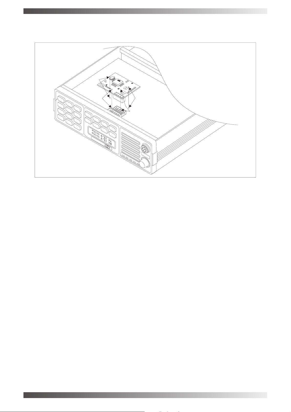
Fitting internal scrambler option
TP24
BARRETT 900 SERIES TRANSCEIVERS
TP9
TP12
TP15
BARRETTBARRETT
B
S
U
M
A
B
S
L
950
X
R
X
T
VOL
N
O
PAGE 47
Page 48
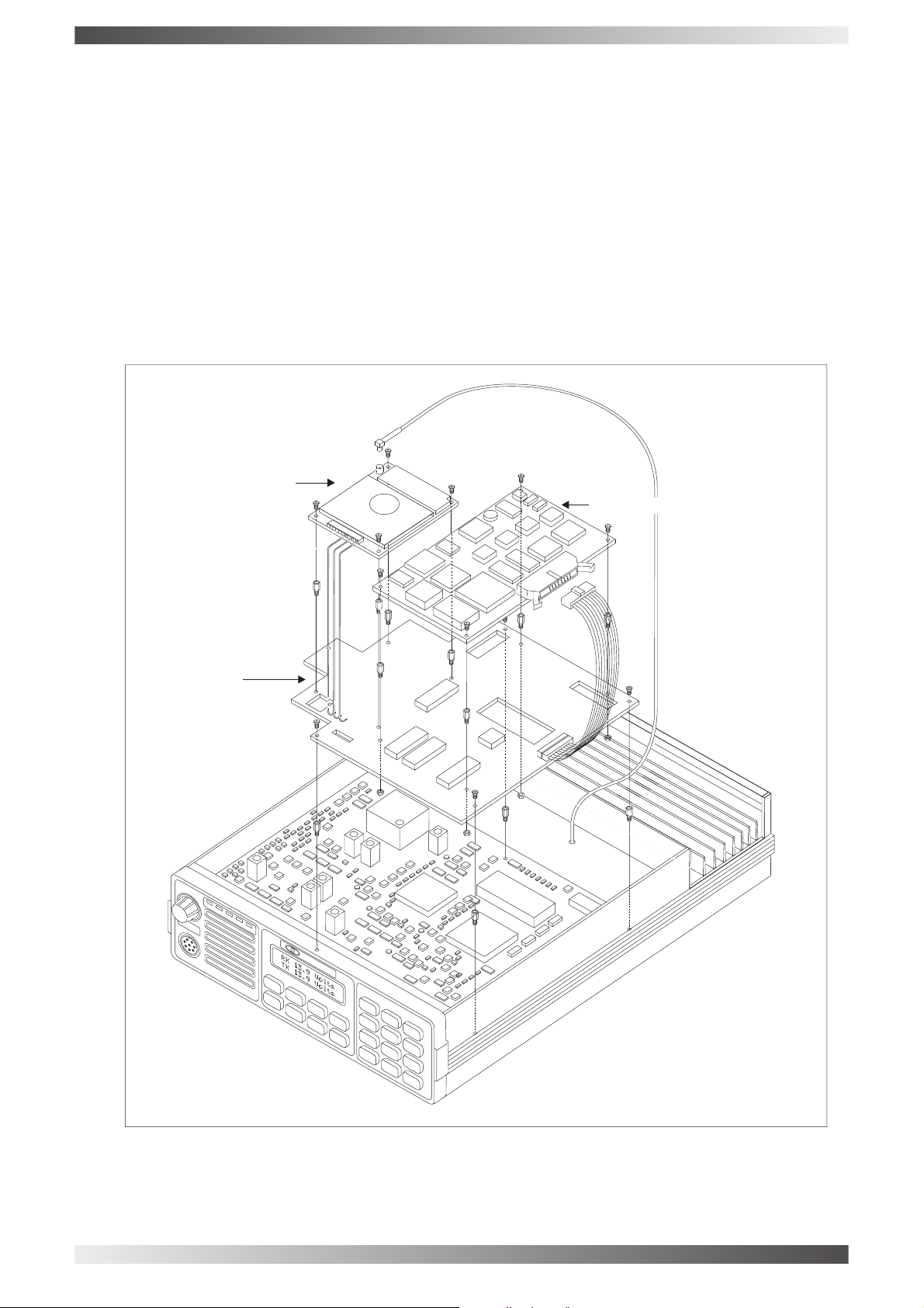
BARRETT 900 SERIES TRANSCEIVERS
8.2 Internal GPS receiver option
P/N BCA90030 available for 950 and 980 transceivers
-
The GPS receiver is mounted on the ALE/GPS mother board which in turn is mounted on the
microprocessor PCB, using the screws and stand-offs supplied, and plugged into the 14 way connector
GPS1. The coaxial cable from the GPS receiver module is routed to the rear of the transceiver, as indicated
in the attached diagram, and terminated on the BNC connector fitted in the normally blanked hole next to the
RF connector on the rear of the transceiver. Note:- ALE option PCB is also fitted on this ALE/GPS
motherboard if required.
8.3 Internal ALE option
P/N BCA95001 and BCA95002 available for 950 transceiver
-
The ALE option PCB is mounted on the ALE/GPS daughter board, which in turn is mounted on the
microprocessor PCB, using the screws and stand-offs supplied, and plugged into the 14 way connector
GPS1. Note:- GPS receiver optionPCB isalso fitted on this ALE/GPSdaughter boardif required.
GPS Receiver
Assembly: 7410
ALE Board Assembly: 7510
ALE/GPS Daughter Board
Assembly: 9912
O
N
VOL
T
X
R
X
L
S
B
A
950
M
U
S
B
BARRETTBARRETT
PAGE 48
Page 49

BARRETT 900 SERIES TRANSCEIVERS
9.0 Features and configurations unique to transceiver models
9.1 Barrett 950 transceivers fitted with high stability option - P/N BC95001 and
BC95003
These transceivers are fitted with a high stability TCXO/DCXO but are otherwise identical to 950
transceivers. The high stability option isdocumented on the microprocessor schematic and PCBoverlay.
9.2 Barrett 950M transceiver module - P/N BC95004
The Barrett 950M is technically identical to the Barrett 950 local control transceiver, without a front panel
fitted. It is supplied standard with GAL Level 3 which enables RS-232 control and is fitted with a high
stability TCXO/DCXO.
The Barrett 950M is primarily for use with the Barrett 960 telephone interconnect but can be used in a
variety of remote control applications wherea basic HF transceiver module is required.
9.3 Barrett 950MR receivers - P/N BC95005 / BC95006
The Barrett 950MR and Barrett 950MR1 are technically identical to the Barrett 950 local control
transceiver, but have a PCB fitted in place of the PA PCB containing low pass filters, power relay
circuitry and antenna switch components. The Barrett 950MR P/N BC95005 is fitted with a normal 950
local control front panel and canbe programmed through this front panel orvia the RS-232 port. The Barrett
950MR1 P/N BC95006 is housed ina 1U standard 19" rack mount cabinet.It has no control panel and is
intended for control and programming via its RS-232 port. Both receivers are fitted with high stability
TCXO/DCXO's.
PAGE 49
Page 50
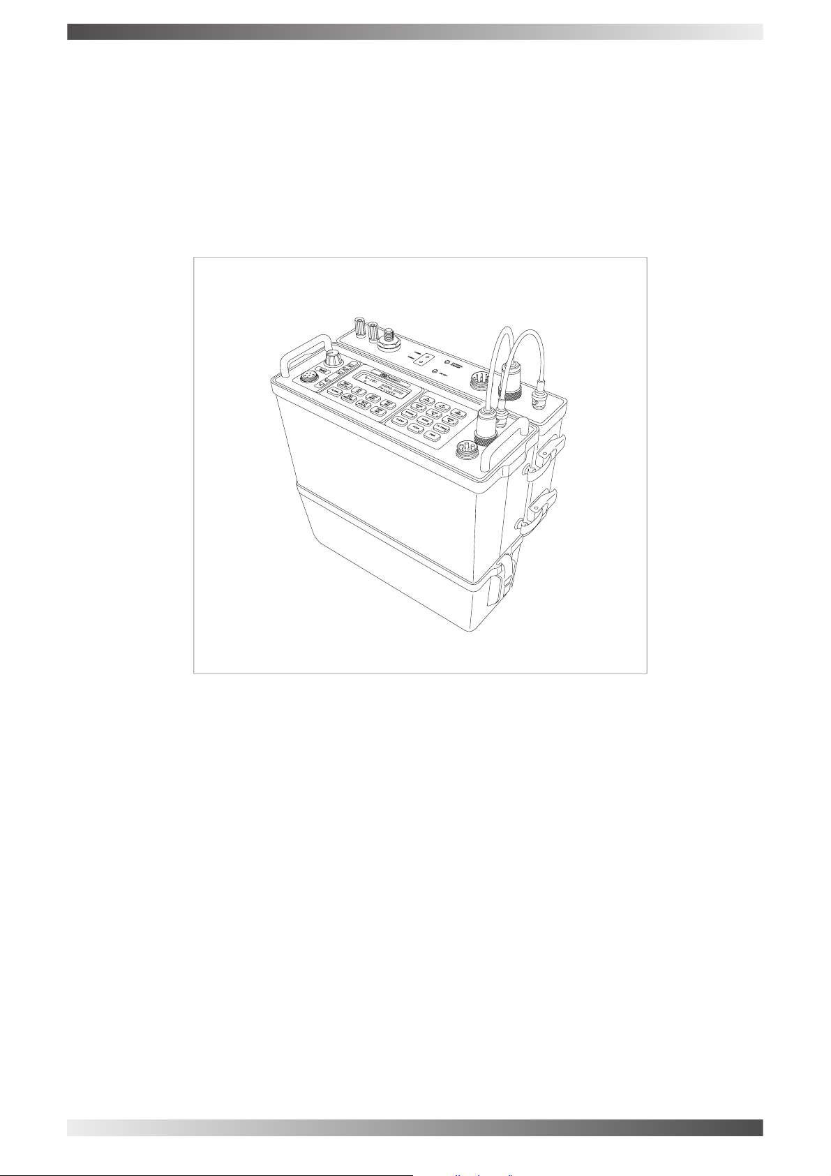
BARRETT 900 SERIES TRANSCEIVERS
9.4 Barrett 940 man-pack - P/N BC94001
The Barrett 940 man-pack is technically identical to the Barrett 950 but has the PA set between 10 and
35 W output. In addition it is fitted with the high stability TCXO/DCXO as standard and has a switch
mode regulator fitted to the microprocessor PCB in place of the normal regulators for low power
consumption purposes. A connector transitionPCB provides a microphone amplifier for the handset
connector and transition from the IDCcable to the military waterproof front panelconnectors. The 9 4 0 is
constructed in a water resistant case and has a battery pack that clips on the rear of the transceiver. In its
portable form an accessory cover isprovided that fits over the front panelwhen in transit.
9.4.1 940 ancillary components
9.4.1.1 110to 240 VAC input chargersupply BarrettP/N BCA94012
The BCA94012 Input Charger Supply is an AC/DC switch-mode power supply that provides a regulated 16V
output from an AC power sourceof between 90V and 264V.
9.4.1.2 Charge regulator suit 13AhNiMH battery12V DC input Barrett P/NBCA94021
The BCA94021 NiMH 12V input charge regulator charges the BCA94008 battery with a constant current
source of approximately 2.5A. This source is regulated by U4:A, Q9 and R30. The source is pulsed or
switched off by the battery charge controller U3 using Q5. The current source is pulsed to look for a voltage
drop which indicates the battery is fully charged. The current source is switched off if the battery is fully
charged or a fault condition occurs. A fault condition is where the battery voltage is over 14.7V or under 7.4V
or where battery temperature is over 54C or under -9C. This temperature is measured by a thermistor inside
the battery pack.
The charging section is provided with power from two possible sources. The first is regulated external DC
input of 16V provided, usually, by a charger supply Barrett P/N BCA94012. This input is over-voltage and
reverse voltage protectedby a relay. The second is unregulated DC inputwith an input range between 10.8V
and 15.6V. This is over-voltage, under-voltage and reverse voltage protected by a relay and supplies a
switch mode power supply to provide16V to the charging section.
PAGE 50
Page 51

BARRETT 900 SERIES TRANSCEIVERS
The switch mode power supply is of a standard design. The FET Q1, when switched on, pulls current
through an inductor L2 to ground. When Q1 is switched off, this current then flows through the diode D3 and
powers the output. The output voltage is higher than the input but to maintain continuity in the current
through L2 the voltage must increase. Thus the voltage increase at the output of D3, when related to the
input of L2, is defined by the duty cycle of Q1. This duty cycle is controlled by the switch mode controller U1.
The input and output of thiscircuit are filtered to eliminate EMI.
9.4.1.3 940 multiple-use distribution unitBarrett P/NBCA94010
The BCA94010 multiple-use distribution unit provides simultaneous access for a CW key, headphones,
13.8V power input and programming functionfor the 940 transceiver.
9.4.1.4 940 automatic antenna tuner
Introduction
The Barrett 940 MkII Tuner is designed to interface the 940 portable transceiver to either a vertical whip
or a long wire antenna. The tuner requires only a power input, a RF feed and a tune line which when
pulled to ground will initiate a tune command.
Tuning Network
The whip antenna is resonant at approximately 23MHz. Below resonance the whip presents a
capacitive reactance which needs to be tuned out with inductance. A binary network of inductors from
0.33µH to 84µH are used to give a total of 168µH. This is required for tuning at the lowest frequency.
When the whip is operated above resonance or there is a long wire connected a series capacitor (C1)
and two shunt capacitors (C10 & C11) are used to present a capacitive load. Any residual capacitance
is then removed by the inductive network.
To minimise the current draw of the unit all relays are latching. Low voltage relays are used to switch the
smaller coils whilst the larger value coils which produce the larger voltages (>500V) have the higher
spec G2R relays to switch them out of circuit. To minimise the contact voltages the largest inductor is
split into two smaller inductances of 42µH(L9 and L10). After a tune is performed the power supply to
the latching relays is removed. This increases the RF impedance to earth which minimises the chances
of a flash over from contact to coil.
Pad and Phase Detector
A -10dB pad is switched in during the tuning procedure by RL12. The pad has the function of reducing
the RF voltage to minimise arcing and to present a resistive load to the transmitter so that it can provide
a full 20W during tuning. Whenever the pad is used a phase detector is also switched in. This
comprises of a current sense transformer (T3) and a voltage sense capacitor (C33). These two signals
are mixed and rectified via a diode network and generate a DC voltage whose polarity directly relates to
either leading or lagging load. The signal is converted to TTL by comparator U8 and is sent to the micro.
Current Sense
The usefulness of the phase detector is limited to below quarter wavelength resonance so for tuning
above this a 10:1 current transformer (T1) is employed. The current sensor measures the RF current
flowing into the tuning network. The maximum current into this network should directly correspond to the
minimum transmitter VSWR. The output of the current transformer is rectified and is sampled by the
microprocessor.
Impedance transformer
Once any whip or long wire reactance has been cancelled the impedance transformer is used find the
best VSWR. Two relays (RL15 and RL16) and a tapped inductor (T2) are used to give three different
impedance transforms (1:2, 1:1 and 2:1). This covers an impedance range of 12.5 to 200 . The
appropriate transform ratio is chosen depending on which delivers the most current through the current
sense network.
Microprocessor
A PIC16C73 microprocessor is responsible for controlling all operations of the tuner. A pair of shift
registers (U4 and U5) are used to expand the external relays the micro can drive. The micro addresses
the relays in a serial fashion.
To reduce current consumption the microprocessor will put the tuner into scan mode and go to sleep
after a period of two minutes. Any burst of RF will wake the micro up again so that it may come out of
scan mode or may tune again. The microprocessor can directly measure the frequency of the input RF
via a diode network (D3-D5) and a capacitor sense (C13). If the frequency is the same then the
previous tune condition is restored. If the frequency is different then another tune will be attempted.
PAGE 51
Page 52

BARRETT 900 SERIES TRANSCEIVERS
Tuning Algorithm
A tune is initiated by pulling the tune line low whilst simultaneously sending RF. By default the tuner
assumes that the whip looks capacitive. Firstly it will find a starting inductor, determined by whichever
inductor makes the whip look slightly inductive, and then initiate a binary search algorithm. Once this is
completed the impedance transformer will attempt to match the whip to the transmitter by switching its three
impedance ratios and optimising the RF feed current. If this current is not high enough the binary search
algorithm is reinitiated with series capacitor C1 switched in. This takes care of the whip above resonance
where the inductance is small. The impedance transformer will try to match the whip to the transmitter to
give highest feed current.
If the feed current is not high enough the tuner assumes that a long wire antenna is connected. Generally
use of the long wire will involve tuning out much larger inductances so shunt capacitors C2 and C3 are
employed to make the wire appear slightly capacitive. Since the required reactance to tune out this residual
capacitance will be small, a sequential tuning algorithm is employed using only the smaller tuning inductors.
The combination which produces the highest feed current is assumed to be the optimum. Finally the
impedance transformer will attempt to match the resistive component of the long wire to the transmitter.
Tuning time will vary from half a second to four seconds depending on whether a whip or long wire is used.
Specifications
Current Draw
Static: < 20mA
Tune: 500mA (Max).
Supply Voltage: 10V - 15V.
Input Power
Maximum input Power: 25W
Operating Frequency: 2.5MHz - 30MHz (8ft whip)
2MHz - 30MHz (Long wire)
Tuning Time: 1s-4s.
Maximum output Voltage: <2kV.
9.5 Barrett 980 GMDSS transceiver - P/N BC98000
The Barrett 980 GMDSS transceiver is technically identical to the Barrett 950L but has a high stability
oscillator and a 500Hz filter for F1B (AFSK) operation fitted as standard. It can also be supplied with a 300 W
switch mode power supply fitted in a standard 900 series enclosure. This switch mode power supply has an
input voltage of 24 VDC and provides galvanic isolation of the transceiver from the power as required by
GMDSS regulations.
PAGE 52
Page 53
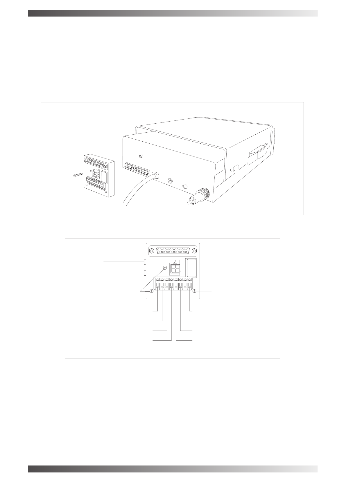
BARRETT 900 SERIES TRANSCEIVERS
10.0 Accessory interface unit - P/N BCA90016
The accessory interface unit is used to enable easy access to various functions available on the rear
accessory connector of930, 950and 980 series transceivers. The unit allows access to an external speaker
or headphones and a CW key via standard 3.5 mm jack sockets. A 4 way "Minifit" socket is provided for the
910 Automatic tuning mobile antenna or 911 Automatic Antenna tuner. A set of screw terminals is provided
to allow an external GPS to be connected as well as an external alarm and cross mute connection. The full
25 way accessory connector is duplicated by the connector on the accessory interface to enable data and
other ancillary products to be connectedusing the standard Barrett 25 way cables(P/N BCA90021/22).
CW Key
Headphones
Securing Screws
+13VDC-2Amps max
EXT. GPS NMEA HIGH
EXT. GPS NMEA LOW
Ground
Automatic antennas
or tuners, 510/910
511/911
Securing Screws
EXT. SPEAKER
CW KEY
EXT.ALM N/O
EXT. ALM.COMMON
PAGE 53
Page 54

11.0 Auxiliary connector
11.1 Barrett 980 and Barrett 950 transceivers
BARRETT 900 SERIES TRANSCEIVERS
Pin Name Description of function Level Option required
1 Ground Ground 0V None
2 Rx Data RS-232 data input True RS-232 BCO95003
3 Tx Data RS-232 data output True RS-232 BCO95003
4 External Power On For use with Barrett 960 or ancilliary equipment. Low to activate None
5 External Speaker External speaker output 0-10V None
6 Tuned In Antenna tune cycle complete input from 910 / 911 Low going pulse None
7 RS-232 Gnd. RS-232 Ground 0V None
8 ALC / Ext. GPS In Ext. ALC from Linear Amp / Ext. GPS Input (with pin 20) 0-10V / NMEA 0183 BCO95002/3
9 Auxiliary PTT In Auxiliary PTT input Low to activate PTT None
10 Scan Stop Scan stop input from external modem Low to stop scan None
11 Bal. Tx Audio In Balanced external Tx audio input (with pin 24) 600 Ohms 0dBm. None
12 Bal. Rx Audio Out Balanced un-muted Rx audio output (with pin 25) 600 Ohms 0dBm. None
13 Ground Ground 0V None
14 Ant 0 / Pre-amp on Channel no. output Octal bit 0 / 910 pre-amp on Active low None
15 Ant 1 Channel no. output Octal bit 1 Active low None
16 Ant 2 Channel no. output Octal bit 2 Active low None
17 External Alarm Out / Horn / Latched alarm out (selcall activated) Active low BCO95002/3
Ant 3 Channel no. output Octal bit 3
18 13.8 V Int Out Interrupted 13.8 V for 910 Auto. Antenna 13.8V-0V None
19 Ant 0 / Pre-amp on 910 pre-amp on / Channel no. output Octal bit 0 Active low None
- Note 2
- Note 2
- Note 2
- Note 2
/
- Note 2
to activate
20 FSK / Ext. GPS in FSK digital input / Ext. GPS Input (with pin 8) Active low / NMEA BCO95002/3
21 PTT / C-Mute Out PTT Out / Receiver Cross Mute Out Active low None
22 CW Key Input from CW Key Low to activate None
23 +13.8 V Fused Out +13.8V Output to power auxilliary equipment 13.8V @ 2 Amp. None
24 Bal. Tx Audio In Balanced external Tx audio input (with pin 11) 600 Ohms 0dBm. None
25 Bal. Rx Audio Out Balanced un-muted Rx audio output (with pin 12) 600 Ohms 0dBm. None
Note 1:- Pin 8 and Pin20 - External GPS inputis selected using a menufunction or set duringprogramming when the software optionrequired is fitted.
Note 2:- These outputs provide channel information for use with antenna select units such as the BARRETT 916. The outputs are octal coded 0 to FF
representing the least significant digit of the channel number selected. i.e. octal 0 for channel 1, octal 1 for channels 2, octal 3 for channels 2, to
octal FF for channel 16/
0183
PAGE 54
Page 55

11.2 Barrett 930 transceivers
BARRETT 900 SERIES TRANSCEIVERS
Pin Name Description of function Level Option required
1 Ground Ground 0V None
2 Rx Data RS-232 data input(for cloning/programming function only) True RS-232 None
3 Tx Data RS-232 data output(for cloning/programming function only) True RS-232 None
4 External Power On For use with Barrett 960 or ancillary equipment. Low to activate None
5 External Speaker External speaker output 0-10V None
6 Tuned In Antenna tune cycle complete input from 910 / 911 Low going pulse None
7 RS-232 Gnd. RS-232 Ground (for cloning function only) 0V None
8 ALC Ext. ALC from Linear Amp 0-10V None
9 Auxiliary PTT In Auxiliary PTT input Low to activate PTT None
10 Scan Stop Scan stop input from external modem Low to stop scan None
11 Bal. Tx Audio In Balanced external Tx audio input (with pin 24) 600 Ohms 0dBm. None
12 Bal. Rx Audio Out Balanced un-muted Rx audio output (with pin 25) 600 Ohms 0dBm. None
13 Ground Ground 0V None
14 Ant 0 / Pre-amp on Channel no. output Octal bit 0 / 910 pre-amp on Active low None
15 Ant 1 Channel no. output Octal bit 1 Active low None
16 Ant 2 Channel no. output Octal bit 2 Active low None
17 External Alarm Out Horn / Latched alarm out (selcall activated) Active low BCO93002
18 13.8 V Int Out / Ant 3 Interrupted 13.8 V for 910 Auto. Antenna / Ant 3 13.8V-0V / Active Low None
19 Ant 0 / Pre-amp on 910 pre-amp on / Channel no. output Octal bit 0 Active low None
20 N/C N/C N/C None
21 PTT / C-Mute Out PTT Out / Receiver Cross Mute Out Active low None
22 CW Key Input from CW Key Low to activate None
23 +13.8 V Fused Out +13.8V Output to power auxilliary equipment 13.8V @ 2 Amp. None
24 Bal. Tx Audio In Balanced external Tx audio input (with pin 11) 600 Ohms 0dBm. None
25 Bal. Rx Audio Out Balanced un-muted Rx audio output (with pin 12) 600 Ohms 0dBm. None
to activate
Note1:- These outputs provide channel information for use with antenna select units such as the BARRETT 916. The outputs are octal coded 0
to FF representing the least significant digit of the channel number selected. i.e. octal 0 for channel 1, octal 1 for channels 2, octal 3 for
channels 2, to octal FFfor channel 16.
PAGE 55
Page 56
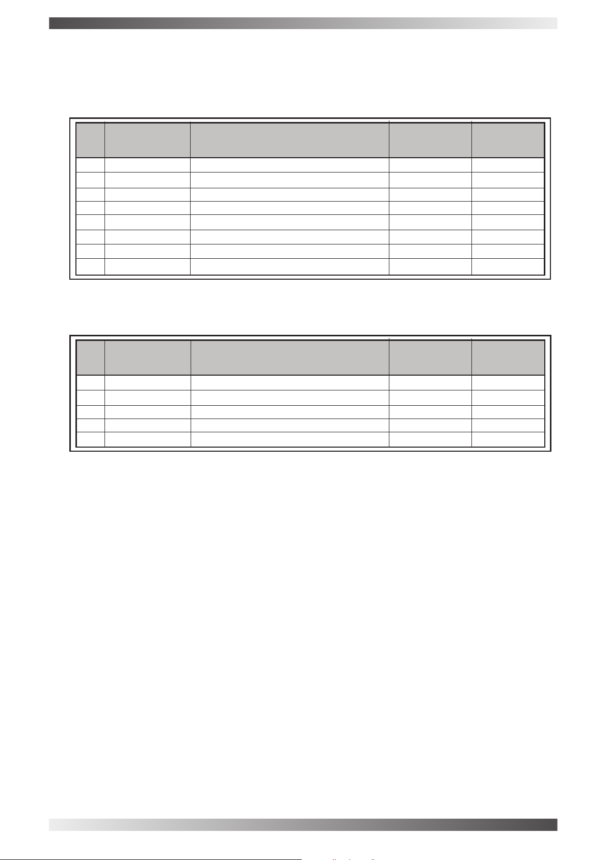
11.3 Barrett 940 manpack transceivers
Barrett 940 manpack portable transceiver P/N BC94000 / BC94001
8 pin waterproof panel mounted plug
BARRETT 900 SERIES TRANSCEIVERS
Pin Name Description of function Level Option required
1 Ground Ground 0V None
2 Rx Data RS-232 data input (for cloning/programming function only) True RS-232 None
3 Tx Data RS-232 data output (for cloning function only) True RS-232 None
4 CW key CW key input Ground to activate None
5 External Speaker External speaker output 0-10V None
6 Tune command Antenna tune command to 940 automatic tuner option Low going pulse None
7 +13.8VDC External power input - positive +13.8 VDC None
8 +13.8VDC Power output to 940 tuner +13.8 VDC None
5 pin waterproof panel mounted socket
Pin Name Description of function Level Option required
1 Ground Ground 0 V None
2 Speaker Speaker output 0-10 V None
3 PTT Transmit key. Ground to activate None
4 Mic in Microphone input 10mV None
5 CW key CW key input Ground to activate None
to activate
to activate
PAGE 56
Page 57
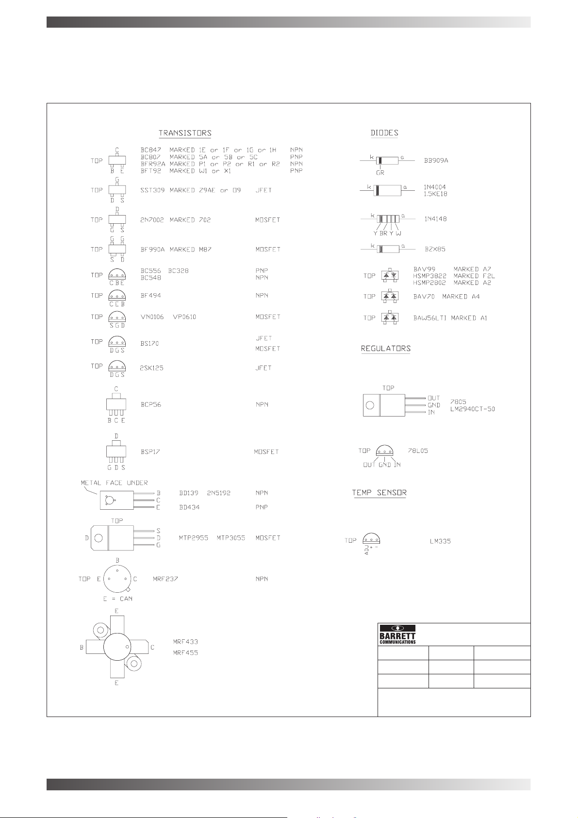
12.0 Circuit diagrams, overlays and parts lists
Active component outlines
BARRETT 900 SERIES TRANSCEIVERS
DRAWING NUMBER
900S109A0.PCB
SCALE
NTS
DRAWN
DJS(PE)
DRAWING TITLE
DATE
3-2-99
DIMENSIONING
DESIGNED
RAG KAE
DISCRETE SEMICONDUCTORS
IN BARRETT 900 SERIES TRANSCEIVERS
ECN REFERENCE
BARRETT PART NO
SHEET
1OF1
PAGE 57
Page 58
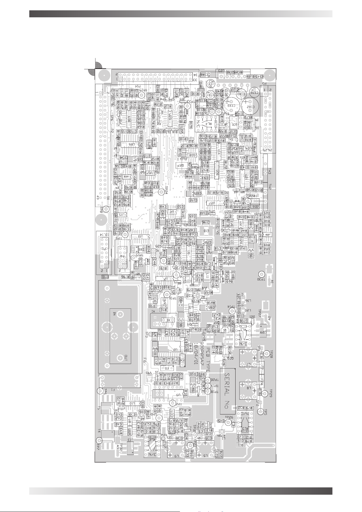
BARRETT 900 SERIES TRANSCEIVERS
RF/Audio PCB overlay - showing optional narrow filter components.
PAGE 58
Page 59

BARRETT 900 SERIES TRANSCEIVERS
RF-AUDIO Schematic - Showing optional narrow filter components.
See File: RF-AUDIO-BOARD-SCHEMATICS.pdf
PAGE 59
Page 60

This page has been intentionally left blank
BARRETT 900 SERIES TRANSCEIVERS
PAGE 60
Page 61

BARRETT 900 SERIES TRANSCEIVERS
BARRETT 900 RF/AUDIO BOARD PARTS LIST
---------------------------------------------------------------------------------------------------------------------------------------PCB P/N: PC-900P85A7
Issue A7 Sheet 1 of 11
Assembly P/N: SA-09933
---------------------------------------------------------------------------------------------------------------------------------------COMPONENT DESCRIPTION BARRETT COMMENTS
DESIGNATOR P/N
-----------------------------------------------------------------------------------------------------------------------------
-----------
C1 CAP SMD 1206 0.1uF CP-00916
C2 CAP SMD 1206 1.0uF CERAMIC CP-00908
C3 CAP SMD 0805 1nF CP-00915
C4 CAP SMD 1206 33nF CP-00953
C5 CAP SMD 0805 1nF CP-00915
C6 CAP SMD 0805 10pF CP-00936
C7 CAP SMD 0805 1nF CP-00915
C8 CAP SMD 0805 33pF CP-00928
C9 CAP SMD 0805 1nF CP-00915
C10 CAP SMD 1206 0.1uF CP-00916
C11 CAP SMD TANT 10uF 16V CP-01580
C12 CAP SMD 0805 12pF CP-00923
C13 CAP SMD 0805 12pF CP-00923
C14 CAP SMD 1206 0.1uF CP-00916
C15 CAP SMD 1206 0.1uF CP-00916
C16 CAP SMD 1206 0.1uF CP-00916
C17 CAP SMD 1206 0.1uF CP-00916
C18 CAP SMD 1206 0.1uF CP-00916
C19 CAP SMD 1206 0.1uF CP-00916
C20 CAP SMD 1206 0.1uF CP-00916
C21 CAP SMD 0805 15 pF CP-00938
C22 CAP SMD 1206 10nF CP-00951
C23 CAP SMD 1206 10nF CP-00951
C24 CAP SMD 0805 2p2F CP-00918
C25 CAP SMD 0805 1nF CP-00915
C26 CAP SMD 0805 1nF CP-00915
C27 CAP SMD TANT 1uF 16V CP-01570
C28 CAP SMD 0805 1nF CP-00915
C29 CAP SMD 1206 47nF CP-00954
C30 CAP SMD 1206 1.0uF CERAMIC CP-00908
C31 CAP SMD 0805 8p2F CP-00935
C32 CAP SMD 1206 10nF CP-00951
C33 CAP SMD 1206 10nF CP-00951
C34 CAP SMD 0805 1nF CP-00915
C35 CAP SMD 0805 1nF CP-00915
C36 CAP SMD 0805 8p2F CP-00935
C37 CAP SMD 0805 6p8F CP-00919
C38 CAP SMD TANT 10uF 16V CP-01580
C39 CAP SMD 1206 0.1uF CP-00916
C40 CAP SMD 1206 0.1uF CP-00916
C41 CAP SMD 1206 0.1uF CP-00916
C42 CAP SMD TANT 10uF CP-01580
C43 CAP SMD 1206 1.0uF CERAMIC CP-00908
C44 CAP SMD 1206 10nF CP-00951
C45 CAP SMD 0805 1nF CP-00915
C46 CAP SMD TANT 10uF 16V CP-01580
C47 CAP SMD 1206 0.1uF CP-00916
C48 CAP SMD 1206 10nF CP-00951
C49 CAP SMD 1206 10nF CP-00951
C50 CAP SMD 1206 0.1uF CP-00916
PAGE 61
Page 62

BARRETT 900 SERIES TRANSCEIVERS
BARRETT 900 RF/AUDIO BOARD PARTS LIST
---------------------------------------------------------------------------------------------------------------------------------------PCB P/N: PC-900P85A7 Issue A7 Sheet 2 of 11
Assembly P/N: SA-09933
---------------------------------------------------------------------------------------------------------------------------------------COMPONENT DESCRIPTION BARRETT COMMENTS
DESIGNATOR P/N
----------------------------------------------------------------------------------------------------------------------------------------
C51 CAP SMD 0805 1nF CP-00915
C52 CAP SMD 1206 10nF CP-00951
C53 CAP SMD 10uF TANT CP-01580
C54 CAP SMD 1206 0.1uF CP-00916
C55 CAP SMD 1206 10nF CP-00951
C56 CAP SMD 10uF TANT CP-01580
C57 CAP SMD 1206 0.1uF CP-00916
C58 CAP SMD 1206 0.1uF CP-00916
C59 CAP SMD 1206 0.1uF CP-00916
C60 CAP SMD 1206 1.0uF CERAMIC CP-00908
C61 CAP SMD 0805 1nF CP-00915
C62 CAP SMD 1206 1.0uF CERAMIC CP-00908
C63 CAP SMD 1206 0.1uF CP-00916
C64 CAP SMD 1206 0.1uF CP-00916
C65 CAP SMD 1206 0.1uF CP-00916
C66 CAP SMD 1206 0.1uF CP-00916
C67 CAP SMD 1206 0.1uF CP-00916
C68 CAP SMD 1206 0.1uF CP-00916
C69 CAP SMD 1206 0.1uF CP-00916
C70 CAP SMD 1206 0.1uF CP-00916
C71 CAP SMD 1206 0.1uF CP-00916
C72 CAP SMD 1206 1.0uF CERAMIC CP-00908
C73 CAP SMD 1206 0.1uF CP-00916
C74 CAP SMD 1206 0.1uF CP-00916
C75 CAP SMD 1206 0.1uF CP-00916
C76 CAP SMD 0805 1nF CP-00915
C77 CAP SMD TANT 10uF 16V CP-01580
C78 CAP SMD TANT 10uF 16V CP-01580
C79 CAP SMD 1206 0.1uF CP-00916
C80 CAP SMD 0805 1nF CP-00915
C81 CAP SMD TANT 22uF 20V CP-01590
C82 CAP SMD 0805 1nF CP-00915
C83 CAP SMD 1206 0.1uF CP-00916
C84 CAP SMD TANT 10uF 16V CP-01580
C85 CAP SMD 1206 0.1uF CP-00916
C86 CAP SMD 1206 0.1uF CP-00916
C87 CAP SMD 1206 10nF CP-00951
C88 CAP SMD 1206 1.0uF CERAMIC CP-00908
C89 CAP SMD 1206 1.0uF CERAMIC CP-00908
C90 CAP SMD 1206 2u2F CERAMIC CP-00909
C91 CAP SMD 1206 0.1uF CP-00916
C92 CAP SMD 1206 0.1uF CP-00916
C93 CAP SMD TANT 10uF 16V CP-01580
C94 CAP SMD 0805 120pF CP-00939
C95 CAP SMD TANT 10uF 16V CP-01580
C96 CAP SMD 1206 2u2F CERAMIC CP-00909
C97 CAP SMD 0805 1nF CP-00915
C98 CAP SMD 0805 27pF CP-00926
C99 CAP SMD TANT 10uF 16V CP-01580
C100 CAP SMD 0805 1nF CP-00915
PAGE 62
Page 63

BARRETT 900 SERIES TRANSCEIVERS
BARRETT 900 RF/AUDIO BOARD PARTS LIST
---------------------------------------------------------------------------------------------------------------------------------------PCB P/N: PC-900P85A7 Issue A7 Sheet 3 of 11
Assembly P/N: SA-09933
---------------------------------------------------------------------------------------------------------------------------------------COMPONENT DESCRIPTION BARRETT COMMENTS
DESIGNATOR P/N
----------------------------------------------------------------------------------------------------------------------------------------
C101 CAP SMD 0805 15pF CP-00938
C102 CAP SMD 0805 180pF CP-00943
C103 CAP SMD 0805 39pF CP-00927
C104 CAP SMD 0805 100pF CP-00940
C105 CAP SMD TANTALUM 10uF 16V CP-01580
C106 CAP SMD 1206 0.1uF CP-00916
C107 CAP SMD TANT 1uF 16V CP-01570
C108 CAP SMD 1206 1uF CERAMIC CP-00908
C109 CAP SMD 1206 0.1uF CP-00916
C110 CAP SMD 0805 4n7 CP-10947
C111 CAP SMD 0805 4n7 CP-10947
C112 CAP SMD 1206 0.1uF CP-00916
C113 CAP SMD 0805 1nF CP-00915
C114 CAP SMD 1206 0.1uF CP-00916
C115 CAP SMD 1206 0.1uF CP-00916
C116 CAP SMD 1206 0.1uF CP-00916
C117 CAP SMD 1206 2n2 CP-00937
C118 CAP SMD 0805 1nF CP-00915
C119 CAP SMD 1206 0.1uF CP-00916
C120 CAP SMD 0805 4n7 CP-10947
C121 CAP SMD 0805 4n7 CP-10947
C122 CAP SMD 1206 0.1uF CP-0 0916
C123 CAP SMD TANT 10uF 16V CP-01580
C124 CAP SMD 1206 1uF CERAMIC CP-00908
C125 CAP SMD 1206 1uF CERAMIC CP-00908
C126 CAP SMD 1206 0.1uF CP-00916
C127 CAP SMD 1206 0.1uF CP-00916
C128 CAP 100uF 25V RB CP-01637
C129 CAP SMD 1206 1uF CERAMIC CP-00908
C130 CAP SMD TANT 1.0uF 16V CP-01570
C131 CAP SMD 0805 1nF CP-00915
C132 CAP SMD 1206 0.1uF CP-00916
C133 CAP 470uF 16V RB CP-01755
C134 CAP SMD 1206 0.1uF CP-00916
C135 CAP 100uF 25V RB CP-01637
C136 CAP SMD 1206 1uF CERAMIC CP-00908
C137 CAP SMD 1206 0.1uF CP-00916
C138 CAP SMD 1206 0.1uF CP-00916
C139 CAP 100uF 25V RB CP-01637
C140 CAP 100uF 25V RB CP-01637
C141 CAP 100uF 25V RB CP-01637
C142 CAP 470uF 16V RB CP-01755
C143 CAP SMD 1206 0.1uF CP-00916
C144 CAP SMD 1206 1uF CERAMIC CP-00908
C145 CAP SMD 1206 0.1uF CP-00916
C146 CAP SMD TANT 10uF 16V CP-01580
C147 CAP SMD 1206 0.1uF CP-00916
C148 CAP SMD 1206 0.1uF CP-00916
C149 CAP SMD 1206 0.1uF CP-00916
C150 CAP SMD 1206 0.1uF CP-00916
PAGE 63
Page 64

BARRETT 900 SERIES TRANSCEIVERS
BARRETT 900 RF/AUDIO BOARD PARTS LIST
---------------------------------------------------------------------------------------------------------------------------------------PCB P/N: PC-900P85A7 Issue A7 Sheet 4 of 11
Assembly P/N: SA-09933
---------------------------------------------------------------------------------------------------------------------------------------COMPONENT DESCRIPTION BARRETT COMMENTS
DESIGNATOR P/N
----------------------------------------------------------------------------------------------------------------------------------------
C151 CAP SMD 1206 2n2F CP-00937
C152 CAP SMD 1206 0.1uF CP-00916
C153 CAP SMD 1206 0.1uF CP-00916
C154 CAP SMD 0805 1nF CP-00915
C155 CAP SMD 1206 0.1uF CP-00916
C156 CAP SMD 1206 0.1uF CP-00916
C157 CAP SMD TANT 10uF 16V CP-01580
C158 CAP SMD 1206 1.0uF CERAMIC CP-00908
C159 CAP SMD 1206 1uF CERAMIC CP-00908
C160 CAP SMD 1206 1uF CERAMIC CP-00908
C161 CAP SMD 1206 1uF CERAMIC CP-00908
C162 CAP SMD 1206 10nF CP-00951
C163 CAP SMD 1206 1uF CERAMIC CP-00908
C164 CAP SMD 1206 10nF CP-00951
C165 CAP SMD 10uF TANT CP-01580
C166 CAP SMD 1206 0.1uF CP-00916
C167 CAP SMD 1206 0.1uF CP-00916
C168 CAP SMD 0805 1nF CP-00915
C169 CAP SMD 1206 1uF CERAMIC CP-00908
C170 CAP SMD 1206 2u2F CERAMIC CP-00909
C171 CAP SMD 1206 0.1uF CP-00916
C172 CAP SMD 1206 1uF CERAMIC CP-00908
C173 CAP SMD 1206 10nF CP-00951
C174 CAP SMD 0805 1nF CP-00915
C175 CAP SMD 1206 0.1uF CP-00916
C176 CAP SMD 1206 0.1uF CP-00916
C177 CAP SMD 1206 0.1uF CP-00916
C178 CAP SMD 0805 1nF CP-00915
C179 CAP SMD 0805 1nF CP-00915
C180 CAP SMD 1206 0.1uF CP-00916
C181 CAP SMD 0805 1nF CP-00915
C182 CAP SMD 1206 0.1uF CP-00916
C183 CAP SMD 1206 0.1uF CP-00916
C184 CAP SMD 1206 15nF CP-00972
C185 CAP SMD 1206 0.1uF CP-00916
C186 CAP SMD 1206 0.1uF CP-00916
C187 CAP SMD 1206 0.1uF CP-00916
C188 CAP SMD 1206 0.1uF CP-00916
C189 CAP SMD 1206 0.1uF CP-00916
C190 CAP SMD 1206 0.1uF CP-00916
C191 CAP SMD 1206 0.1uF CP-00916
C192 CAP SMD 1206 0.1uF CP-00916
C193 CAP SMD 1206 15nF CP-00972
C194 CAP SMD 1206 0.1uF CP-00916
C195 CAP SMD 1206 0.1uF CP-00916
C196 CAP SMD 0805 270pf CP-00911
C198 CAP SMD 1206 1uF CERAMIC CP-00908
C199 CAP SMD 1206 0.1uF CP-00916
C202 CAP SMD 1206 1uF CERAMIC CP-00908
C203 CAP SMD 1206 1uF CERAMIC CP-00908
PAGE 64
Page 65

BARRETT 900 SERIES TRANSCEIVERS
BARRETT 900 RF/AUDIO BOARD PARTS LIST
---------------------------------------------------------------------------------------------------------------------------------------PCB P/N: PC-900P85A7 Issue A7 Sheet 5 of 11
Assembly P/N: SA-09933
---------------------------------------------------------------------------------------------------------------------------------------COMPONENT DESCRIPTION BARRETT COMMENTS
DESIGNATOR P/N
----------------------------------------------------------------------------------------------------------------------------------------
C204 CAP SMD 1206 0.1uF CP-00916
C205 CAP SMD 1206 0.1uF CP-00916
C206 CAP SMD 1206 0.1uF CP-00916
C207 CAP SMD 1206 1uF CERAMIC CP-00908
C208 CAP SMD 1206 0.1uF CP-00916
D1 DIODE SMD BAV 99 DI-03317
D2 DIODE SMD BAV 70 DI-03316
D3 DIODE SMD BAV 70 DI-03316
D4 DIODE SMD BAV 70 DI-03316
D5 DIODE SMD BAV 70 DI-03316
D6 DIODE SMD BAV 70 DI-03316
D7 DIODE SMD BAV 70 DI-03316
D8 DIODE SMD BAV 70 DI-03316
D9 DIODE SMD BAV99 DI-03317
D10 DIODE SMD BAW56 DI-03300
D11 DIODE SMD BAW56 DI-03300
D12 DIODE SMD BAV 70 DI-03316
D13 DIODE SMD BAV 70 DI-03316
D14 DIODE SMD BAV 99 DI-03317
D15 DIODE SMD BAV 70 DI-03316
D16 DIODE SMD BAV 99 DI-03317
D17 DIODE SMD BAV 70 DI-03316
D18 DIODE SMD BAV 70 DI-03316
D19 DIODE SMD BAV 99 DI-03317
D20 DIODE SMD BAV 99 DI-03317
D21 DIODE SMD BAV 70 DI-03316
D22 DIODE SMD BAV 70 DI-03316
F1 CERAMIC FILTER CFJ455K5 FI-07604
F2, F2A CRYSTAL FILTER PAIR 45MHz FI-07603
F4 CERAMIC FILTER CFSFE 10.7 FI-07601
F5 CERAMIC FILTER CFSFE 10.7 FI-07601
F6 OPTIONALFILTER 455 KHz 500Hz X00F05A FI-07602
J1 2 PIN PLUG POLARISED CN-14101
L1 CHOKE SMD 470nH IN-15002
L2 CHOKE SMD 100 uH IN-03601
L3 CHOKE SMD 1uH IN-03590
L4 CHOKE SMD 10uH IN-03600
L5 COIL F772 IN-03215
L7 COIL F772 IN-03215
L8 COIL F772 IN-03215
L9 COIL F772 IN-03215
L10 CHOKE 470uH SMD IN-15004
L11 CHOKE 1mH SMD IN-03585
L16 CHOKE 270nH SMD IN-15000
L18 CHOKE SMD 100 uH IN-03601
L19 CHOKE SMD 100 uH IN-03601
L20 CHOKE 220nH SMD IN-15001
L21 CHOKE SMD 100uH IN-03601
L22 CHOKE SMD 100uH IN-03601
L23 CHOKE SMD 100uH IN-03601
L24 CHOKE SMD 100uH IN-03601
L25 CHOKE SMD 100uH IN-03601
PAGE 65
Page 66

BARRETT 900 SERIES TRANSCEIVERS
BARRETT 900 RF/AUDIO BOARD PARTS LIST
---------------------------------------------------------------------------------------------------------------------------------------PCB P/N: PC-900P85A7 Issue A7 Sheet 6 of 11
Assembly P/N: SA-09933
---------------------------------------------------------------------------------------------------------------------------------------COMPONENT DESCRIPTION BARRETT COMMENTS
DESIGNATOR P/N
----------------------------------------------------------------------------------------------------------------------------------------
L27 CHOKE SMD 100uH IN-03601
P1 HEADER BOX 14 PIN CN-04144
P2 HEADER SOCKET 50 PIN CN-04218
P3 HEADER BOX 26 WAY CN-04121
P4 HEADER BOX 10 PIN CN-04138
P14 HEADER BOX 34 PIN CN-04139
Q1 MOS FET 2N7000 PHILIPS TR-02284
Q2 FET SMD 2N7002 LT-1 TR-02282
Q3 FET SMD 2N7002 LT-1 TR-02282
Q4 FET SMD BF990A TR-02219
Q5 FET SMD BF990A TR-02219
Q6 TRANSISTOR SMD BC847 TR-02262
Q7 FET SMD 2N7002 LT-1 TR-02282
Q8 TRANSISTOR SMD BC847 TR-02262
Q9 FET SMD 2N7002 LT-1 TR-02282
Q10 TRANSISTOR SMD BC847 TR-02262
Q11 TRANSISTOR SMD BC807 TR-02229
Q12 TRANSISTOR SMD BC807 TR-02229
Q13 TRANSISTOR SMD BC807 TR-02229
Q14 TRANSISTOR SMD BC847 TR-02262
Q15 FET SMD 2N7002 LT-1 TR-02282
Q16 FET POWER IRF7404 TR-00001
Q17 TRANSISTOR SMD BC847 TR-02262
Q18 FET SMD MMBF545 TR-02238
Q19 FET SMD 2N7002 LT-1 TR-02282
Q20 FET SMD 2N7002 LT-1 TR-02282
Q21 FET SMD 2N7002 LT-1 TR-02282
Q22 FET SMD 2N7002 LT-1 TR-02282
Q23 FET SMD 2N7002 LT-1 TR-02282
Q24 TRANSISTOR SMD BC807 TR-02229
Q25 TRANSISTOR SMD BC847 TR-02262
Q26 TRANSISTOR SMD BC807 TR-02229
Q27 FET SMD BSP17 TR-02207
Q28 TRANSISTOR SST309 TR-02259
Q29 FET SMD 2N7002 LT-1 TR-02282
Q30 TRANSISTOR SMD BC807 TR-02229
Q31 TRANSISTOR SMD BC807 TR-02229
Q32 FET SMD 2N7002 LT-1 TR-02282
Q33 FET SMD 2N7002 LT-1 TR-02282
R1 RES SMD 1206 10R RE-00111
R2 RES SMD 1206 1K RE-00122
R3 RES SMD 1206 33R RE-00112
R4 RES SMD 1206 470R RE-00121
R6 RES SMD 1206 47K RE-00157
R7 RES SMD 1206 10K RE-00150
R8 RES SMD 1206 470R RE-00121
R9 RES SMD 1206 470R RE-00121
R10 RES SMD 1206 10R RE-00111
R11 RES SMD 1206 10R RE-00111
R12 RES SMD 1206 10R RE-00111
R13 RES SMD 1206 470R RE-00121
R14 RES SMD 1206 1R0 RE-00090
PAGE 66
Page 67

BARRETT 900 SERIES TRANSCEIVERS
BARRETT 900 RF/AUDIO BOARD PARTS LIST
---------------------------------------------------------------------------------------------------------------------------------------PCB P/N: PC-900P85A7 Issue A7 Sheet 7 of 11
Assembly P/N: SA-09933
---------------------------------------------------------------------------------------------------------------------------------------COMPONENT DESCRIPTION BARRETT COMMENTS
DESIGNATOR P/N
----------------------------------------------------------------------------------------------------------------------------------------
R15 RES SMD 1206 100K RE-00170
R16 RES SMD 1206 1R0 RE-00090
R17 RES SMD 1206 10K RE-00150
R18 RES SMD 1206 2K2 RE-00125
R19 RES SMD 1206 1K5 RE-00124
R20 RES SMD 1206 5K6 RE-00129
R21 RES SMD 1206 1K0 RE-00122
R22 RES SMD 1206 10R RE-00111
R23 RES SMD 1206 47K RE-00157
R24 RES SMD 1206 4K7 RE-00128
R25 RES SMD 1206 100K RE-00170
R26 RES SMD 1206 10K RE-00150
R27 RES SMD 1206 47K RE-00157
R28 RES SMD 1206 47K RE-00157
R29 RES SMD 1206 10R RE-00111
R30 RES SMD 1206 5M6 RE-00185
R31 RES SMD 1206 10K RE-00150
R32 RES SMD 1206 100R RE-00117
R33 RES SMD 1206 10K RE-00150
R34 RES SMD 1206 4K7 RE-00128
R35 RES SMD 1206 180R RE-00118
R36 RES SMD 1206 47K RE-00157
R37 RES SMD 1206 10K RE-00150
R38 RES SMD 1206 680R RE-00101
R39 RES SMD 1206 10K RE-00150
R40 RES SMD 1206 22R RE-00108
R41 RES SMD 1206 10R RE-00111
R42 RES SMD 1206 18K RE-00152
R43 RES SMD 1206 47K RE-00157
R44 RES SMD 1206 22K RE-00153
R45 RES SMD 1206 12K RE-00149
R46 RES SMD 1206 470R RE-00121
R47 RES SMD 1206 680R RE-00101
R48 RES SMD 1206 470R RE-00121
R49 RES SMD 1206 1 5K RE-00151
R50 RES SMD 1206 10K RE-00150
R51 RES SMD 1206 330K RE-00176
R52 RES SMD 1206 10K RE-00150
R53 RES SMD 1206 10K RE-00150
R55 RES SMD 1206 20K RE-00010
R56 RES SMD 1206 100R RE-00117
R57 RES SMD 1206 2K2 RE-00125
R58 RES SMD 1206 4K7 RE-00128
R59 RES SMD 1206 3K3 RE-00127
R60 RES SMD 1206 2K7 RE-00126
R61 RES SMD 1206 2K7 RE-00126
R62 RES SMD 1206 330R RE-00107
R63 RES SMD 1206 56R RE-00114
R64 RES SMD 1206 56R RE-00114
R65 RES SMD 1206 220R RE-00119
R66 RES SMD 1206 220R RE-00119
R67 RES SMD 1206 150R RE-00138
PAGE 67
Page 68

BARRETT 900 SERIES TRANSCEIVERS
BARRETT 900 RF/AUDIO BOARD PARTS LIST
---------------------------------------------------------------------------------------------------------------------------------------PCB P/N: PC-900P85A7 Issue A7 Sheet 8 of 11
Assembly P/N: SA-09933
---------------------------------------------------------------------------------------------------------------------------------------COMPONENT DESCRIPTION BARRETT COMMENTS
DESIGNATOR P/N
----------------------------------------------------------------------------------------------------------------------------------------
R68 RES SMD 1206 820R RE-00102
R69 RES SMD 1206 33K RE-00155
R70 RES SMD 1206 10K RE-00150
R71 RES SMD 1206 100R RE-00117
R72 RES SMD 1206 680R RE-00101
R73 RES SMD 1206 10K RE-00150
R74 RES SMD 1206 15K RE-00151
R75 RES SMD 1206 10K RE-00150
R76 RES SMD 1206 10R RE-00111
R77 RES SMD 1206 6K8 RE-00259
R78 RES SMD 1206 22K RE-00265
R79 RES SMD 1206 12R RE-00070
R80 RES SMD 1206 10K RE-00150
R81 RES SMD 1206 10K RE-00150
R82 RES SMD 1206 10K RE-00150
R83 RES SMD 1206 6K8 RE-00130
R84 RES SMD 1206 2K2 RE-00125
R85 RES SMD 1206 4K7 RE-00128
R86 RES SMD 1206 10R RE-00111
R87 RES SMD 1206 10K RE-00150
R88 RES SMD 1206 4K7 RE-00128
R89 RES SMD 1206 100K RE-00170
R90 RES SMD 1206 1K1 RE-10267
R91 RES SMD 1206 750R RE-10268
R92 RES SMD 1206 560R RE-00132
R93 RES SMD 1206 10K RE-00261
R94 RES SMD 1206 10K RE-00261
R95 RES SMD 1206 1K8 RE-00252
R96 RES SMD 1206 1K8 RE-00252
R97 RES SMD 1206 100K RE-00170
R98 RES SMD 1206 22K RE-00153
R99 RES SMD 1206 100K RE-00170
R100 RES SMD 1206 1M0 RE-00178
R101 RES SMD 1206 100K RE-00170
R102 RES SMD 1206 12K RE-10261
R103 RES SMD 1206 12K RE-10261
R104 RES SMD 1206 1K2 RE-00123
R105 RES SMD 1206 4R7 RE-00092
R106 RES SMD 1206 33K RE-00267
R107 RES SMD 1206 100R RE-00117
R108 RES SMD 1206 1K0 RE-00122
R109 RES SMD 1206 1M0 RE-00178
R110 RES SMD 1206 10K RE-00150
R111 RES SMD 1206 1M0 RE-00178
R112 RES SMD 1206 10K RE-00150
R113 RES SMD 1206 100R RE-00117
R114 RES SMD 1206 10K RE-00150
R115 RES SMD 1206 10K RE-00150
R116 RES SMD 1206 100K RE-00170
R117 RES SMD 1206 1M0 RE-00178
R118 RES SMD 1206 39K RE-00156
R119 RES SMD 1206 22K RE-00153
PAGE 68
Page 69

BARRETT 900 SERIES TRANSCEIVERS
BARRETT 900 RF/AUDIO BOARD PARTS LIST
---------------------------------------------------------------------------------------------------------------------------------------PCB P/N: PC-900P85A7 Issue A7 Sheet 9 of 11
Assembly P/N: SA-09933
---------------------------------------------------------------------------------------------------------------------------------------COMPONENT DESCRIPTION BARRETT COMMENTS
DESIGNATOR P/N
----------------------------------------------------------------------------------------------------------------------------------------
R120 RES SMD 1206 10K RE-00150
R121 RES SMD 1206 68K RE-00158
R122 RES SMD 1206 68K RE-00158
R123 RES SMD 1206 47K RE-00269
R124 RES SMD 1206 47K RE-00157
R125 RES SMD 1206 10K RE-00150
R126 RES SMD 1206 1K0 RE-00122
R127 RES SMD 1206 8K2 RE-00260
R128 RES SMD 1206 10K RE-00150
R129 RES SMD 1206 1M0 RE-00178
R130 RES SMD 1206 10K RE-00150
R131 RES SMD 1206 6K8 RE-00130
R132 RES SMD 1206 1K0 RE-00122
R133 RES SMD 1206 180K RE-00173
R134 RES SMD 1206 2R7 RE-00103
R135 RES SMD 1206 4R7 RE-00092
R136 RES SMD 1206 4K7 RE-00128
R137 RES SMD 1206 1K2 RE-00123
R138 RES SMD 1206 220K RE-00174
R139 RES SMD 1206 10K RE-00150
R140 RES SMD 1206 18K RE-00152
R141 RES SMD 1206 2M2 RE-00187
R142 RES SMD 1206 330K RE-00176
R143 RES SMD 1206 330K RE-00176
R144 RES SMD 1206 2R7 RE-00103
R145 RES SMD 1206 120K RE-00184
R146 RES SMD 1206 10K RE-00150
R147 RES SMD 1206 10K RE-00150
R148 RES SMD 1206 4K7 RE-00128
R149 RES SMD 1206 220K RE-00174
R150 RES SMD 1206 39K RE-00268
R151 RES SMD 1206 5K6 RE-00129
R152 RES SMD 1206 10K RE-00150
R153 RES SMD 1206 100R RE-00117
R154 RES SMD 1206 10K RE-00150
R155 RES SMD 1206 100R RE-00117
R156 RES SMD 1206 100K RE-00170
R157 RES SMD 1206 120K RE-00174
R158 RES SMD 1206 100K RE-00170
R159 RES SMD 1206 5K6 RE-00129
R161 RES SMD 1206 100R RE-00117
R162 RES SMD 1206 100R RE-00117
R163 RES SMD 1206 100R RE-00117
R164 RES SMD 1206 100R RE-00117
R165 RES SMD 1206 100K RE-00170
R166 RES SMD 1206 10R RE-00111
R167 RES SMD 1206 10K RE-00150
R168 RES SMD 1206 10K RE-00150
R169 RES SMD 1206 100K RE-00170
R170 RES SMD 1206 100K RE-00170
R171 RES SMD 1206 1M0 RE-00178
R172 RES SMD 1206 10K RE-00150
PAGE 69
Page 70

BARRETT 900 SERIES TRANSCEIVERS
BARRETT 900 RF/AUDIO BOARD PARTS LIST
---------------------------------------------------------------------------------------------------------------------------------------PCB P/N: PC-900P85A7 Issue A7 Sheet 10 of 11
Assembly P/N: SA-09933
---------------------------------------------------------------------------------------------------------------------------------------COMPONENT DESCRIPTION BARRETT COMMENTS
DESIGNATOR P/N
----------------------------------------------------------------------------------------------------------------------------------------
R173 RES SMD 1206 4K7 RE-00128
R174 RES SMD 1206 10K RE-00150
R175 RES SMD 1206 6K8 RE-00130
R176 RES SMD 1206 27K RE-00154
R177 RES SMD 1206 10K RE-00150
R178 RES SMD 1206 100K RE-00170
R179 RES SMD 1206 68K RE-00158
R180 RES SMD 1206 68K RE-00158
R181 RES SMD 1206 4K7 RE-00128
R182 RES SMD 1206 1M0 RE-00178
R183 RES SMD 1206 1M0 RE-00178
R184 RES SMD 1206 100K RE-00170
R185 RES SMD 1206 47R RE-00113
R186 RES SMD 1206 4K7 RE-00128
R187 RES SMD 1206 1K RE-00122
R188 RES SMD 1206 10K RE-00150
R189 RES SMD 1206 1M0 RE-00178
R190 RES SMD 1206 10K RE-00150
R191 RES SMD 1206 10K RE-00150
R192 RES SMD 1206 10K RE-00150
R193 RES SMD 1206 1K RE-00122
R194 RES SMD 1206 1K RE-00122
R195 RES SMD 1206 4K7 RE-00128
R196 RES SMD 1206 10K RE-00150
R197 RES SMD 1206 1K0 RE-00122
R198 RES SMD 1206 4K7 RE-00128
R199 RES SMD 1206 4K7 RE-00128
R200 RES SMD 1206 10K RE-00150
R201 RES SMD 1206 390R RE-00120
R202 RES SMD 1206 130R RE-00096
R203 RES SMD 1206 47R RE-00113
R204 RES SMD 1206 130R RE-00096
R205 RES SMD 1206 2K2 RE-00125
R206 RES SMD 1206 10K RE-00150
R207 RES SMD 1206 1K RE-00122
R208 RES SMD 1206 120K RE-00184
R209 RES SMD 1206 10K RE-00150
R210 RES SMD 1206 1K RE-00122
R211 RES SMD 1206 1K RE-00122
R212 RES SMD 1206 1K RE-00122
R213 RES SMD 1206 10R RE-00111
R214 RES SMD 1206 22K RE-00153
R215 RES SMD 1206 330K RE-00176
R216 RES SMD 1206 10K RE-00150
R217 RES SMD 1206 5K6 RE-00129
R218 RES SMD 1206 270K RE-00180
R219 RES SMD 1206 51K RE-00011
R220 RES SMD 1206 4K7 RE-00128
R221 RES SMD 1206 3K6 RE-00012
R222 RES SMD 1206 10K RE-00150
R227 RES SMD 1206 100K RE-00170
R228 RES SMD 1206 22K RE-00153
PAGE 70
Page 71

BARRETT 900 SERIES TRANSCEIVERS
BARRETT 900 RF/AUDIO BOARD PARTS LIST
---------------------------------------------------------------------------------------------------------------------------------------PCB P/N: PC-900P85A7 Issue A7 Sheet 11 of 11
Assembly P/N: SA-09933
---------------------------------------------------------------------------------------------------------------------------------------COMPONENT DESCRIPTION BARRETT COMMENTS
DESIGNATOR P/N
----------------------------------------------------------------------------------------------------------------------------------------
R229 RES SMD 1206 10K RE-00150
R230 RES SMD 1206 180K RE-00173
R231 RES SMD 1206 5K6 RE-00129
R232 RES SMD 1206 47R RE-00113
R233 RES SMD 1206 47R RE-00113
R234 RES SMD 1206 1M0 RE-00178
RL1 RELAY EA2-12 NEC RL-05013
RL2 RELAY EA2-12 NEC RL-05013
RL3 RELAY EA2-12 NEC RL-05013
RL4 RELAY EA2-12 NEC RL-05013
T1 T/FORM SMD T-622-KK81 IC-02766
T4 OPTIONALT/FORM SMD T36-1-KK81 MCL IC-02768
T6 T/FORM SMD T36-1-KK81 MCL IC-02768
TH1 THERMISTOR PHILIPS PTC TH-02555
TH2 THERMISTOR PTC C945 TH-02545
TH3 THERMISTOR PTC C945 TH-02545
U2 IC SMD SA605D IC-02713
U4 IC SMD MC1350 IC-02709
U5 IC SMD LM358M IC-02706
U6 IC SMD MC1496D IC-02718
U7 IC SMD 4053 IC-02720
U8 IC SMD NE630 IC-02734
U9 IC LM 319 IC-02715
U10 IC SMD 74HC132 IC-02708
U11 IC SMD 4053 IC-02720
U12 IC SMD NE630 IC-02734
U13 BAL MIXER RFLMS-1-RM6 IC-20000
U14 IC SMD 4053 IC-02720
U15 IC SMD LMC6042 IC-02777
U16 IC SMD 4053 IC-02720
U17 IC SMD LMC6042 IC-02777
U18 IC SMD LMC6082 IC-02800
U19 IC SMD LM 358M IC-02706
U21 IC SMD 4053 IC-02720
U22 IC SMD LMC6042 IC-02777
U23 IC TDA 2004 IC-02736
U24 IC SMD LMC6042 IC-02777
U25 IC SMD 74HC14 IC-02738
U26 IC SMD ST232ACT IC-02732
U27 IC SMD 4053 IC-02720
U28 IC SMD MC1350 IC-02709
U29 BAL MIXER RFLMS-1-13-RM6 IC-NEW
U30 IC SMD ULN2003 IC-02717
U31 IC 4N35 IC-02460
U32 IC SMD MC1350 IC-02709
U33 IC LMC6082 SMD IC-02800
VR1 TRIMPOT SMD 100K IC-02515
VR2 TRIMPOT SMD 1K IC-02513
VR4 TRIMPOT SMD 100K IC-02515
X1 SAW RESONATOR 55.7MHz FI-07621
Z1 ZENER 4.7V SMD SOT-23 DI-03304
PAGE 71
Page 72
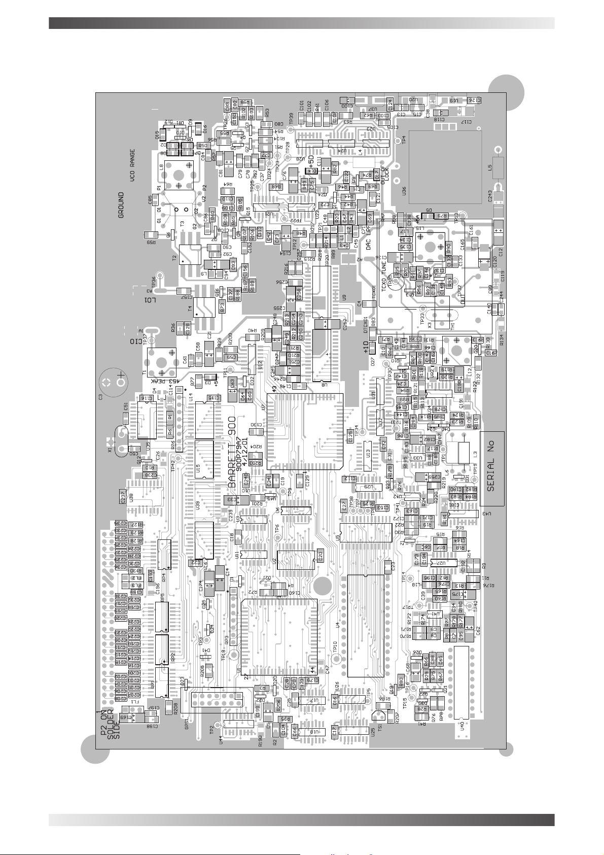
Microprocessor PCB overlay - showing TCXO.
BARRETT 900 SERIES TRANSCEIVERS
PAGE 72
Page 73

BARRETT 900 SERIES TRANSCEIVERS
Microprocessor Schematic - Showing optional switch mode regulator (940) and TCXO.
See File: MICRO-BOARD SCHEMATIC.pdf
PAGE 73
Page 74

This page has been intentionally left blank
BARRETT 900 SERIES TRANSCEIVERS
PAGE 74
Page 75

BARRETT 900 SERIES TRANSCEIVERS
BARRETT 900 MICRO BOARD PARTS LIST
---------------------------------------------------------------------------------------------------------------------------------------PCB P/N: PC-900P79A7 Issue A7 Sheet 1 of 12
Assembly P/N: SA-09929 DTCXO/LinReg (DLR)
SA-09931 XTAL/LinReg (XLR)
SA-09932 DTCXO/SMPS (DSM)
---------------------------------------------------------------------------------------------------------------------------------------COMPONENT DESCRIPTION BARRETT COMMENTS
DESIGNATOR P/N
----------------------------------------------------------------------------------------------------------------------------------------
C3 CAP 470uF 16V ELECTRO RB CP-01755
C4 CAP SMD 1206 0.1uF CP-00916
C5 CAP SMD TANT 2.2uF CP-01620
C6 CAP SMD TANT 1uF CP-01570
C7 CAP SMD 1206 0.1uF CP-00916
C8 CAP SMD 1206 10nF POLY CP-00960
C9 CAP SMD 1206 10nF POLY CP-00960
C10 CAP SMD 1206 0.1uF CP-00916
C11 CAP SMD 1206 0.1uF CP-00916
C12 CAP SMD TANT 10uF CP-01580
C13 CAP SMD TANT 1uF CP-01570
C14 CAP SMD TANT 10uF CP-01580
C15 CAP SMD 1206 0.1uF CP-00916
C16 CAP SMD 1206 0.1uF CP-00916
C17 CAP SMD 1206 0.1uF CP-00916
C18 CAP SMD 1206 0.1uF CP-00916
C19 CAP SMD 1206 0.1uF CP-00916
C20 CAP SMD 1206 0.1uF CP-00916
C21 CAP SMD TANT 10uF CP-01580
C22 CAP SMD 1206 0.1uF CP-00916
C23 CAP SMD 1206 0.1uF CP-00916
C24 CAP SMD 0805 1nF CP-00915
C25 CAP SMD 1206 0.1uF CP-00916
C26 CAP SMD 1206 0.1uF CP-00916
C27 CAP SMD 1206 0.1uF CP-00916
C28 CAP SMD 0805 1nF CP-00915
C31 CAP SMD 1206 0.1uF CP-00916
C32 CAP SMD 1206 10nF CP-00951
C33 CAP SMD TANT 10uF CP-01580
C34 CAP SMD 1206 10nF POLY CP-00960
C35 CAP SMD 1206 10nF POLY CP-00960
C37 CAP SMD 0805 1p5 CP-00920
C38 CAP SMD TANT 1uF CP-01570
C39 CAP SMD 1206 0.1uF CP-00916
C42 CAP SMD 0805 1nF CP-00915
C43 CAP SMD 0805 47pF CP-00930
C45 CAP SMD 0805 120pF CP-00939
C47 CAP SMD 1206 0.1uF CP-00916
C48 CAP SMD 0805 47pF CP-00930
C50 CAP SMD 0805 27pF CP-0026
C51 CAP SMD 0805 27pF CP-00926
C58 CAP SMD 1206 0.1uF CP-00916
C59 CAP SMD 1206 10nF CP-00951
C60 CAP SMD 1206 0.1uF CP-00916
C61 CAP SMD 0805 1nF CP-00915
PAGE 75
Page 76

BARRETT 900 SERIES TRANSCEIVERS
BARRETT 900 MICRO BOARD PARTS LIST
---------------------------------------------------------------------------------------------------------------------------------------PCB P/N: PC-900P79A7 Issue A7 Sheet 2 of 12
Assembly P/N: SA-09929 DTCXO/LinReg (DLR)
SA-09931 XTAL/LinReg (XLR)
SA-09932 DTCXO/SMPS (DSM)
---------------------------------------------------------------------------------------------------------------------------------------COMPONENT DESCRIPTION BARRETT COMMENTS
DESIGNATOR P/N
----------------------------------------------------------------------------------------------------------------------------------------
C62 CAP SMD TANT 10uF CP-01580
C63 CAP SMD TANT 10uF CP-01580
C64 CAP SMD 1206 0.1uF CP-00916
C65 CAP SMD 1206 0.1uF CP-00916
C66 CAP SMD 1206 0.1uF CP-00916
C67 CAP SMD 1206 0.1uF CP-00916
C68 CAP SMD TANT 2u2 CP-01620
C69 CAP SMD 1206 0.1uF CP-00916
C70 CAP SMD 0805 1nF CP-00915
C71 CAP SMD TANT 10uF CP-01580
C72 CAP SMD 1206 0.1uF CP-00916
C73 CAP SMD 1206 0.1uF CP-00916
C74 CAP SMD 0805 1nF CP-00915
C75 CAP SMD 1206 0.1uF CP-00916
C76 CAP SMD TANT 10uF CP-01580
C77 CAP SMD 0805 3p3 CP-00921
C78 CAP SMD 0805 1nF CP-00915
C79 CAP SMD 1206 0.1uF CP-00916
C80 CAP SMD 0805 3p3 CP-00921
C81 CAP SMD TANT 10uF CP-01580
C82 CAP SMD 1206 560nF CP-00913
C83 CAP SMD 1206 2u2 CP-00909
C84 CAP SMD 0805 1nF CP-00915
C85 CAP SMD 0805 56pF CP-00931
C86 CAP SMD 0805 56pF CP-00931
C88 CAP SMD 1206 0.1uF CP-00916
C89 CAP SMD 0805 1nF CP-00915
C90 CAP SMD 1206 0.1uF CP-00916
C92 CAP SMD 0805 1nF CP-00915
C93 CAP SMD 1206 0.1uF CP-00916
C94 CAP SMD TANT 10uF CP-01580
C100 CAP SMD TANT 1uF CP-01570
C101 CAP SMD 0805 1nF CP-00915
C102 CAP SMD 1206 0.1uF CP-00916
C103 CAP SMD 1206 0.1uF CP-00916
C104 CAP SMD 1206 0.1uF CP-00916
C105 CAP SMD 0805 1nF CP-00915
C106 CAP SMD 1206 0.1uF CP-00916
C107 CAP SMD 0805 1nF CP-00915
C108 CAP SMD 0805 1nF CP-00915
C109 CAP SMD 0805 1nF CP-00915
C110 CAP SMD 1206 0.1uF CP-00916
C111 CAP SMD TANT 10uF CP-01580
C112 CAP SMD 1206 0.1uF CP-00916
C113 CAP SMD 0805 1nF CP-00915
PAGE 76
Page 77

BARRETT 900 SERIES TRANSCEIVERS
BARRETT 900 MICRO BOARD PARTS LIST
---------------------------------------------------------------------------------------------------------------------------------------PCB P/N: PC-900P79A7 Issue A7 Sheet 3 of 12
Assembly P/N: SA-09929 DTCXO/LinReg (DLR)
SA-09931 XTAL/LinReg (XLR)
SA-09932 DTCXO/SMPS (DSM)
---------------------------------------------------------------------------------------------------------------------------------------COMPONENT DESCRIPTION BARRETT COMMENTS
DESIGNATOR P/N
----------------------------------------------------------------------------------------------------------------------------------------
C114 CAP SMD TANT 1uF CP-01570
C115 CAP SMD 1206 0.1uF CP-00916
C116 CAP SMD 1206 0.1uF CP-00916
C117 CAP SMD TANT 10uF CP-01580
C118 CAP SMD TANT 1uF CP-01570
C119 CAP SMD 1206 0.1uF CP-00916
C120 CAP TANT 22uF CP-01590
C121 CAP SMD 1206 0.1uF CP-00916
C122 CAP SMD 0805 1nF CP-00915
C123 CAP SMD 0805 1nF CP-00915
C124 CAP SMD 1206 0.1uF CP-00916
C125 CAP SMD 1206 0.1uF CP-00916
C126 CAP SMD 1206 0.1uF CP-00916
C127 CAP SMD 1206 10nF CP-00951
C128 CAP SMD 1206 10nF CP-00951
C129 CAP SMD 1206 0.1uF CP-00916
C130 CAP SMD 1206 0.1uF CP-00916
C131 CAP SMD 0805 1nF CP-00915
C132 CAP SMD 0805 6p8 CP-00919
C133 CAP SMD 0805 6p8 CP-00919
C134 CAP SMD 0805 1nF CP-00915
C135 CAP SMD 1206 0.1uF CP-00916
C136 CAP SMD TANT 10uF CP-01580
C137 CAP SMD 0805 6p8 CP-00919
C138 CAP SMD 1206 0.1uF CP-00916
C139 CAP SMD 0805 1nF CP-00915
C140 CAP SMD 0805 1nF CP-00915
C141 CAP SMD 0805 1nF CP-00915
C142 CAP SMD 0805 1nF CP-00915
C143 CAP SMD 1206 0.1uF CP-00916
C144 CAP SMD 1206 0.1uF CP-00916
C145 CAP SMD 0805 1nF CP-00915
C146 CAP SMD 0805 6p8 CP-00919
C147 CAP SMD 1206 0.1uF CP-00916
C148 CAP SMD 1206 0.1uF CP-00916
C149 CAP SMD 0805 1nF CP-00915
C150 CAP SMD 0805 22nF CP-00904
C152 CAP SMD 0805 1nF CP-00915
C153 CAP SMD 1206 0.1uF CP-00916
C154 CAP SMD TANT 10uF CP-01580
C156 CAP SMD 1206 10nF CP-00951
C157 CAP SMD 1206 10nF CP-00951
C159 CAP SMD 0805 1nF CP-00915
C160 CAP SMD 1206 0.1uF CP-00916
C161 CAP SMD 0805 1nF CP-00915
PAGE 77
Page 78

BARRETT 900 SERIES TRANSCEIVERS
BARRETT 900 MICRO BOARD PARTS LIST
---------------------------------------------------------------------------------------------------------------------------------------PCB P/N: PC-900P79A7 Issue A7 Sheet 4 of 12
Assembly P/N: SA-09929 DTCXO/LinReg (DLR)
SA-09931 XTAL/LinReg (XLR)
SA-09932 DTCXO/SMPS (DSM)
---------------------------------------------------------------------------------------------------------------------------------------COMPONENT DESCRIPTION BARRETT COMMENTS
DESIGNATOR P/N
----------------------------------------------------------------------------------------------------------------------------------------
C162 CAP SMD 0805 1nF CP-00915
C163 CAP SMD 1206 68nF CP-00980
C164 CAP SMD 1206 6n8 CP-00949
C165 CAP SMD 1206 0.1uF CP-00916
C166 CAP SMD 1206 0.1uF CP-00916
C167 CAP SMD 0805 1nF CP-00915
C168 CAP SMD 0805 10pF CP-00936
C169 CAP SMD TANT 10uF CP-01580
C171 CAP SMD 1206 27nF CP-00955
C172 CAP SMD 1206 3n9 CP-00950
C173 CAP SMD 1206 4n7 CP-00947
C174 CAP SMD TANT 10uF CP-01580
C175 CAP SMD TANT 10uF CP-01580
C176 CAP SMD 1206 10nF CP-00951
C178 CAP SMD 1206 0.1uF CP-00916
C179 CAP SMD 1206 0.1uF CP-00916
C180 CAP SMD 1206 10nF CP-00951
C181 CAP SMD TANT 1uF CP-01570
C182 CAP SMD TANT 10uF CP-01580
C183 CAP SMD 1206 0.1uF CP-00916
C184 CAP SMD 1206 33nF CP-00953
C185 CAP SMD 0805 560pF CP-00945
C186 CAP SMD 1206 0.1uF CP-00916
C187 CAP SMD 1206 0.1uF CP-00916
C188 CAP SMD 1206 3n3 CP-00946
C189 CAP SMD 0805 1nF CP-00915
C190 CAP SMD TANT 10uF CP-01580
C191 CAP SMD TANT 1uF CP-01570
C192 CAP SMD 1206 3n3 CP-00946
C193 CAP SMD 0850 1nF CP-00915
C194 CAP SMD 0805 22nF CP-00904
C195 CAP SMD 1206 0.1uF CP-00916
C196 CAP SMD 1206 0.1uF CP-00916
C197 CAP SMD 0850 1nF CP-00915
C198 CAP SMD 1206 0.1uF CP-00916
C199 CAP SMD 1206 0.1uF CP-00916
C201 CAP SMD 0850 1nF CP-00915
C202 CAP SMD 0850 1nF CP-00915
C203 CAP SMD 0850 1nF CP-00915
C204 CAP SMD 0850 1nF CP-00915
C205 CAP SMD 0850 1nF CP-00915
C206 CAP SMD 0850 1nF CP-00915
C207 CAP SMD 0850 1nF CP-00915
C208 CAP SMD 0805 100pF CP-00940
C209 CAP SMD 0850 1nF CP-00915
PAGE 78
Page 79

BARRETT 900 SERIES TRANSCEIVERS
BARRETT 900 MICRO BOARD PARTS LIST
---------------------------------------------------------------------------------------------------------------------------------------PCB P/N: PC-900P79A7 Issue A7 Sheet 5 of 12
Assembly P/N: SA-09929 DTCXO/LinReg (DLR)
SA-09931 XTAL/LinReg (XLR)
SA-09932 DTCXO/SMPS (DSM)
---------------------------------------------------------------------------------------------------------------------------------------COMPONENT DESCRIPTION BARRETT COMMENTS
DESIGNATOR P/N
----------------------------------------------------------------------------------------------------------------------------------------
C210 CAP SMD 0850 1nF CP-00915
C211 CAP SMD 0850 1nF CP-00915
C212 CAP SMD 0850 1nF CP-00915
C213 CAP SMD 0850 1nF CP-00915
C214 CAP SMD 0850 1nF CP-00915
C215 CAP SMD 0850 1nF CP-00915
C216 CAP SMD 0850 1nF CP-00915
C217 CAP SMD 0850 1nF CP-00915
C218 CAP SMD 0850 1nF CP-00915
C219 CAP SMD 0850 1nF CP-00915
C220 CAP SMD 0850 1nF CP-00915
C221 CAP SMD 0850 1nF CP-00915
C222 CAP SMD 0850 1nF CP-00915
C223 CAP SMD 0850 1nF CP-00915
C224 CAP SMD 0850 1nF CP-00915
C225 CAP SMD 0850 1nF CP-00915
C226 CAP SMD 0850 1nF CP-00915
C227 CAP SMD 0850 1nF CP-00915
C228 CAP SMD 0850 1nF CP-00915
C229 CAP SMD 0850 1nF CP-00915
C230 CAP SMD 0850 1nF CP-00915
C231 CAP SMD 0850 1nF CP-00915
C232 CAP SMD 0850 1nF CP-00915
C233 CAP SMD 0850 1nF CP-00915
C234 CAP SMD 0850 1nF CP-00915
C235 CAP SMD 0850 1nF CP-00915
C236 CAP SMD 0850 1nF CP-00915
C237 CAP SMD 1206 0.1uF CP-00916
C238 CAP SMD 1206 0.1uF CP-00916
C239 CAP SMD 1206 0.1uF CP-00916
C240 CAP SMD 1206 0.1uF CP-00916
C241 CAP SMD 1206 0.1uF CP-00916
C243 CAP SMD TANT 10uF CP-01580
C244 CAP SMD 0850 1nF CP-00915
C245 CAP SMD TANT 10uF CP-01580
C246 CAP SMD 1206 0.1uF CP-00916
C247 CAP SMD 1206 0.1uF CP-00916
C248 CAP SMD TANT 10uF CP-01580
C249 CAP SMD 1206 0.1uF CP-00916
C250 CAP SMD 1206 0.1uF CP-00916
C251 CAP SMD 1206 0.1uF CP-00916
C252 CAP SMD TANT 10uF CP-01580
C253 CAP SMD 1206 0.1uF CP-00916
C254 CAP SMD 1206 0.1uF CP-00916
PAGE 79
Page 80

BARRETT 900 SERIES TRANSCEIVERS
BARRETT 900 MICRO BOARD PARTS LIST
---------------------------------------------------------------------------------------------------------------------------------------PCB P/N: PC-900P79A7 Issue A7 Sheet 6 of 12
Assembly P/N: SA-09929 DTCXO/LinReg (DLR)
SA-09931 XTAL/LinReg (XLR)
SA-09932 DTCXO/SMPS (DSM)
---------------------------------------------------------------------------------------------------------------------------------------COMPONENT DESCRIPTION BARRETT COMMENTS
DESIGNATOR P/N
----------------------------------------------------------------------------------------------------------------------------------------
C255 CAP SMD TANT 10uF CP-01580
C256 CAP SMD 1206 0.1uF CP-00916
C257 CAP SMD 1206 0.1uF CP-00916
C258 CAP SMD 1206 0.1uF CP-00916
C259 CAP SMD TANT 10uF CP-01580
DTCXO1 OSC DTCXO 45.455MHz CR-07613
D1 DIODE SMD BAV70 DI-03316
D2 DIODE SMD BB148 DI-03307
D3 DIODE SMD LED YELLOW LE-02921
D4 DIODE SMD BAV70 DI-03316
D5 DIODE SMD LED YELLOW LE-02921
D6 DIODE SMD BB148 DI-03307
D7 DIODE SMD BB148 DI-03307
D8 DIODE SMD BB148 DI-03307
D9 DIODE SMD BAV99 DI-03317
D10 DIODE SMD BAV70 DI-03316
D11 DIODE SMD BAV70 DI-03316
D12 DIODE SMD BAV99 DI-03317
D14 DIODE SMD LED YELLOW LE-02921
D15 DIODE SMD LED GREEN LE-02922
D16 DIODE SMD LED GREEN LE-02922
D17 DIODE SMD LED RED LE-02920
D19 DIODE SMD BAV99 DI-03317
D20 DIODE SMD BAV70 DI-03316
D21 DIODE SMD BAV99 DI-03317
D22 DIODE SMD BAV70 DI-03316
D23 DIODE SMD BAV99 DI-03317
D24 DIODE SMD BAV70 DI-03316
D25 DIODE SMD BAV70 DI-03316
D26 DIODE SMD BAV99 DI-03317
D27 DIODE SMD LED YELLOW LE-02921
D31 DIODE SMD BAV99 DI-03317
D32 DIODE SMD BAV99 DI-03317
D39 DIODE SMD BAV70 DI-03316
D40 DIODE SMD BAV99 DI-03317
D41 DIODE SMD BAV70 DI-03316
FL1 MURATA FILTER M103 FI-07618
FL2 MURATA FILTER M103 FI-07618
FL3 MURATA FILTER M103 FI-07618
GPS1 CONN 14 PIN LOW PROFILE CN-04014
L1 CHOKE SMD 10uH IN-03600
L2 CHOKE SMD 10uH IN-03600
L3 CHOKE 10uH IN-03631
L4 CHOKE 10uH IN-03631
L5 CHOKE SMD 100uH IN-03605
PAGE 80
Page 81

BARRETT 900 SERIES TRANSCEIVERS
BARRETT 900 MICRO BOARD PARTS LIST
---------------------------------------------------------------------------------------------------------------------------------------PCB P/N: PC-900P79A7 Issue A7 Sheet 7 of 12
Assembly P/N: SA-09929 DTCXO/LinReg (DLR)
SA-09931 XTAL/LinReg (XLR)
SA-09932 DTCXO/SMPS (DSM)
---------------------------------------------------------------------------------------------------------------------------------------COMPONENT DESCRIPTION BARRETT COMMENTS
DESIGNATOR P/N
----------------------------------------------------------------------------------------------------------------------------------------
L6 CHOKE 10uH IN-03631
L8 COIL A8120DL IN-03218
L9 CHOKE SMD 10uH IN-03600
L12 COIL F747 IN-03217
L15 COIL F747 IN-03217
L17 CHOKE SMD 10uH IN-03600
L18 CHOKE SMD 100uH IN-03605
P2 CONN 50 WAY PLUG MALE CN-04000
Q1 TRANSISTOR SMD BFR92A TR-02260
Q2 TRANSISTOR SMD BFR92A TR-02260
Q3 TRANSISTOR SMD BFR92A TR-02260
Q4 TRANSISTOR SMD BFT92 TR-02280
Q5 TRANSISTOR SMD BFT92 TR-02280
Q6 TRANSISTOR SMD SST309 TR-02259
Q7 TRANSISTOR SMD SST309 TR-02259
Q8 TRANSISTOR SMD BFT92 TR-02280
Q9 TRANSISTOR SMD BC847 TR-02262
Q10 TRANSISTOR SMD BFT92 TR-02280
Q11 TRANSISTOR SMD BFT92 TR-02280
Q12 TRANSISTOR SMD BC847 TR-02262
Q13 TRANSISTOR SMD BC847 TR-02262
Q14 TRANSISTOR SMD BFR92A TR-02260
Q15 TRANSISTOR SMD BFT92 TR-02280
Q16 TRANSISTOR SMD BFR92A TR-02260
Q20 TRANSISTOR SMD BFR92A TR-02260
Q21 TRANSISTOR SMD BC847 TR-02262
Q22 TRANSISTOR SMD BC847 TR-02262
Q23 TRANSISTOR SMD BC847 TR-02262
Q24 TRANSISTOR SMD BC807 TR-02229
R1 RES SMD 1206 10K RE-00150
R2 RES SMD 1206 100K RE-00170
R3 RES SMD 1206 10K RE-00150
R4 RES SMD 1206 10K RE-00150
R6 RES SMD 1206 68K RE-00158
R8 RES SMD 1206 47K 1% RE-00157
R9 RES SMD 1206 1K RE-00122
R10 RES SMD 1206 10K RE-00150
R11 RES SMD 1206 10K RE-00150
R12 RES SMD 1206 100K RE-00170
R13 RES SMD 1206 560R RE-00132
R14 RES SMD 1206 1M RE-00178
R15 RES SMD 1206 10K RE-00150
R16 RES SMD 1206 6K8 RE-00130
R17 RES SMD 1206 68K RE-00158
R18 RES SMD 1206 150K RE-00171
PAGE 81
Page 82

BARRETT 900 SERIES TRANSCEIVERS
BARRETT 900 MICRO BOARD PARTS LIST
---------------------------------------------------------------------------------------------------------------------------------------PCB P/N: PC-900P79A7 Issue A7 Sheet 8 of 12
Assembly P/N: SA-09929 DTCXO/LinReg (DLR)
SA-09931 XTAL/LinReg (XLR)
SA-09932 DTCXO/SMPS (DSM)
---------------------------------------------------------------------------------------------------------------------------------------COMPONENT DESCRIPTION BARRETT COMMENTS
DESIGNATOR P/N
----------------------------------------------------------------------------------------------------------------------------------------
R19 RES SMD 1206 130K RE-00164
R22 RES SMD 1206 130K RE-00164
R24 RES SMD 1206 22K RE-00153
R26 RES SMD 1206 47K RE-00157
R27 RES SMD 1206 39K 1% RE-00005
R28 RES SMD 1206 4K7 RE-00128
R29 RES SMD 1206 10K RE-00150
R30 RES SMD 1206 2K2 RE-00125
R35 RES SMD 1206 47K RE-00157
R36 RES SMD 1206 330R RE-00107
R39 RES SMD 1206 10R RE-00111
R40 RES SMD 1206 4K7 RE-00128
R41 RES SMD 1206 10K RE-00150
R42 RES SMD 1206 33K RE-00155
R43 RES SMD 1206 10K RE-00150
R44 RES SMD 1206 470R RE-00121
R46 RES SMD 1206 47R RE-00113
R47 RES SMD 1206 10R RE-00111
R48 RES SMD 1206 10R RE-00111
R49 RES SMD 1206 10R RE-00111
R50 RES SMD 1206 47R RE-00113
R51 RES SMD 1206 2K7 RE-00126
R52 RES SMD 1206 1K RE-00122
R53 RES SMD 1206 1K RE-00122
R54 RES SMD 1206 2K7 RE-00126
R55 RES SMD 1206 10R RE-00111
R56 RES SMD 1206 10R RE-00111
R57 RES SMD 1206 10R RE-00111
R58 RES SMD 1206 68R RE-00115
R59 RES SMD 1206 47K RE-00157
R60 RES SMD 1206 47K RE-00157
R61 RES SMD 1206 10R RE-00111
R62 RES SMD 1206 10R RE-00111
R63 RES SMD 1206 10R RE-00111
R64 RES SMD 1206 10R RE-00111
R65 RES SMD 1206 1K2 RE-00123
R66 RES SMD 1206 2K2 RE-00125
R67 RES SMD 1206 56K RE-00159
R68 RES SMD 1206 10K RE-00150
R69 RES SMD 1206 180R RE-00118
R70 RES SMD 1206 100R RE-00117
R71 RES SMD 1206 10R RE-00111
R72 RES SMD 1206 1K RE-00122
R73 RES SMD 1206 47K RE-00157
R74 RES SMD 1206 10K RE-00150
PAGE 82
Page 83

BARRETT 900 SERIES TRANSCEIVERS
BARRETT 900 MICRO BOARD PARTS LIST
---------------------------------------------------------------------------------------------------------------------------------------PCB P/N: PC-900P79A7 Issue A7 Sheet 9 of 12
Assembly P/N: SA-09929 DTCXO/LinReg (DLR)
SA-09931 XTAL/LinReg (XLR)
SA-09932 DTCXO/SMPS (DSM)
---------------------------------------------------------------------------------------------------------------------------------------COMPONENT DESCRIPTION BARRETT COMMENTS
DESIGNATOR P/N
----------------------------------------------------------------------------------------------------------------------------------------
R75 RES SMD 1206 10K RE-00150
R76 RES SMD 1206 4K7 RE-00128
R77 RES SMD 1206 1K5 RE-00124
R78 RES SMD 1206 10K RE-00150
R79 RES SMD 1206 1K5 RE-00124
R80 RES SMD 1206 4K7 RE-00128
R82 RES SMD 1206 1K5 RE-00124
R83 RES SMD 1206 3K9 RE-00134
R86 RES SMD 1206 47R RE-00113
R87 RES SMD 1206 3K3 RE-00127
R88 RES SMD 1206 1K2 RE-00123
R89 RES SMD 1206 10R RE-00111
R90 RES SMD 1206 1K8 RE-00133
R91 RES SMD 1206 22K RE-00153
R92 RES SMD 1206 10K RE-00150
R93 RES SMD 1206 56R RE-00114
R94 RES SMD 1206 10R RE-00111
R95 RES SMD 1206 10K RE-00150
R96 RES SMD 1206 56R RE-00114
R97 RES SMD 1206 22K RE-00153
R98 RES SMD 1206 10R RE-00111
R99 RES SMD 1206 10R RE-00111
R100 RES SMD 1206 5K6 RE-00129
R101 RES SMD 1206 180R RE-00118
R102 RES SMD 1206 220R RE-00119
R103 RES SMD 1206 470R RE-00121
R104 RES SMD 1206 470R RE-00121
R105 RES SMD 1206 220R RE-00119
R106 RES SMD 1206 5K6 RE-00129
R107 RES SMD 1206 3K3 RE-00127
R108 RES SMD 1206 22R RE-00108
R109 RES SMD 1206 100K RE-00170
R110 RES SMD 1206 100K RE-00170
R113 RES SMD 1206 10K RE-00150
R114 RES SMD 1206 68K RE-00158
R115 RES SMD 1206 220K RE-00174
R116 RES SMD 1206 680K RE-00175
R117 RES SMD 1206 680K RE-00175
R118 RES SMD 1206 10K RE-00150
R119 RES SMD 1206 100K RE-00170
R120 RES SMD 1206 100K RE-00170
R121 RES SMD 1206 3K9 RE-00134
R122 RES SMD 1206 1M0 RE-00178
R123 RES SMD 1206 100K RE-00170
R124 RES SMD 1206 68K RE-00158
PAGE 83
Page 84

BARRETT 900 SERIES TRANSCEIVERS
BARRETT 900 MICRO BOARD PARTS LIST
---------------------------------------------------------------------------------------------------------------------------------------PCB P/N: PC-900P79A7 Issue A7 Sheet 10 of 12
Assembly P/N: SA-09929 DTCXO/LinReg (DLR)
SA-09931 XTAL/LinReg (XLR)
SA-09932 DTCXO/SMPS (DSM)
---------------------------------------------------------------------------------------------------------------------------------------COMPONENT DESCRIPTION BARRETT COMMENTS
DESIGNATOR P/N
----------------------------------------------------------------------------------------------------------------------------------------
R125 RES SMD 1206 220K RE-00174
R127 RES SMD 1206 100R RE-00117
R128 RES SMD 1206 100R RE-00117
R129 RES SMD 1206 100R RE-00117
R130 RES SMD 1206 100R RE-00117
R131 RES SMD 1206 2K2 RE-00125
R132 RES SMD 1206 270K RE-00180
R133 RES SMD 1206 100R RE-00117
R134 RES SMD 1206 68R RE-00115
R160 RES SMD 1206 120K 1% RE-00007
R165 RES SMD 1206 1Meg 1% RE-00178
R170 RES SMD 1206 820R 1% RE-00004
R171 RES SMD 1206 39K 1% RE-00005
R172 RES SMD 1206 100K 1% RE-00170
R174 RES SMD 1206 680K 1% RE-10175
R176 RES SMD 1206 33K RE-00155
R177 RES SMD 1206 27K RE-00154
R178 RES SMD 1206 1K 1% RE-00006
R179 RES SMD 1206 3K3 RE-00127
R180 RES SMD 1206 10K RE-00150
R181 RES SMD 1206 10K RE-00150
R182 RES SMD 1206 10K RE-00150
R183 RES SMD 1206 10K RE-00150
R184 RES SMD 1206 220K RE-00174
R185 RES SMD 1206 15K RE-00151
R186 RES SMD 1206 10K RE-00150
R187 RES SMD 1206 39R RE-00109
R188 RES SMD 1206 39R RE-00109
R189 RES SMD 1206 12R RE-00070
R190 RES SMD 1206 10K RE-00150
R200 RES SMD 1206 4K7 RE-00128
R201 RES SMD 1206 1K RE-00122
R203 RES SMD 1206 39K RE-00156
R204 RES SMD 1206 100K RE-00170
R205 RES SMD 1206 10K RE-00150
R206 RES SMD 1206 10K RE-00150
R207 RES SMD 1206 10K RE-00150
R208 RES SMD 1206 1M0 RE-00178
R209 RES SMD 1206 10R RE-00111
R210 RES SMD 1206 100R RE-00117
R211 RES SMD 1206 47R RE-00113
R212 RES SMD 1206 2K RE-10269
R213 RES SMD 1206 10R RE-00111
R214 RES SMD 1206 22K RE-00153
R215 RES SMD 1206 47R RE-00113
PAGE 84
Page 85

BARRETT 900 SERIES TRANSCEIVERS
BARRETT 900 MICRO BOARD PARTS LIST
---------------------------------------------------------------------------------------------------------------------------------------PCB P/N: PC-900P79A7 Issue A7 Sheet 11 of 12
Assembly P/N: SA-09929 DTCXO/LinReg (DLR)
SA-09931 XTAL/LinReg (XLR)
SA-09932 DTCXO/SMPS (DSM)
---------------------------------------------------------------------------------------------------------------------------------------COMPONENT DESCRIPTION BARRETT COMMENTS
DESIGNATOR P/N
----------------------------------------------------------------------------------------------------------------------------------------
R216 RES SMD 1206 2K RE-10269
R217 RES SMD 1206 100R RE-00117
R218 RES SMD 1206 0R RE-00000
R219 RES SMD 1206 10K RE-00150
R220 RES SMD 1206 10K RE-00150
RP1 RESISTOR PACK 100R SMD RE-02760
RP2 RESISTOR PACK 100R SMD RE-02760
RP3 RES NETWORK 10K 8PIN RE-00710
RP4 RESISTOR PACK 100R SMD RE-02760
RP5 RESISTOR PACK 100R SMD RE-02760
RP6 RES NETWORK 10K 9PIN RE-00711
T1 T/FORMER RMC41997 IN-03219
T2 T/FORMER T-622-KK81 SMD IC-02766
T3 T/FORMER 4+4/4+4 MICRO TF-03122
T4 T/FORMER T-622-KK81 SMD IC-02766
TCXO1 45.455MHz TXCO CR-07612
TH1 CERAMIC CRYSTAL HEATER CR-07606
U1 IC D78C10AL CPU IC-02741
U2 IC 74HC574 SMD IC-02705
U3 IC 74HC00 SMD IC-02780
U4 IC 27C512 EPROM IC-02772
U5 IC 28C64 EEPROM SMD IC-02714
U6 IC 74HC138 SMD IC-02788
U7 IC Q2334C-50N DDFS SMD IC-02710
U8 IC DAC908 SMD IC-20005
U9 IC DAC908 SMD IC-20005
U10 IC LM358 SMD IC-02706
U11 IC 74HC04 SMD IC-02782
U12 IC DAC0800 SMD IC-02739
U13 IC 74HC4040 SMD IC-02725
U14 IC 74HC574 SMD IC-02705
U15 IC 74HC574 SMD IC-02705
U16 IC 74HC574 SMD IC-02705
U17 IC 74HC74 SMD IC-02786
U18 IC 74HC74 SMD IC-02786
U19 IC 7805 TO-220 IC-02316
U20 IC 7805 TO-220 IC-02316
U21 IC 74AC00 SMD IC-02700
U22 IC 74AC74 SMD IC-02702
U23 IC 74AC74 SMD IC-02702
U24 IC 74AC74 SMD IC-02702
U25 IC 74HC85 SMD IC-02704
U26 IC 74HC74 SMD IC-02786
U27 IC XR2211 SMD IC-02485
U28 IC 74AC74 SMD IC-02702
PAGE 85
Page 86

BARRETT 900 SERIES TRANSCEIVERS
BARRETT 900 MICRO BOARD PARTS LIST
---------------------------------------------------------------------------------------------------------------------------------------PCB P/N: PC-900P79A7 Issue A7 Sheet 12 of 12
Assembly P/N: SA-09929 DTCXO/LinReg (DLR)
SA-09931 XTAL/LinReg (XLR)
SA-09932 DTCXO/SMPS (DSM)
---------------------------------------------------------------------------------------------------------------------------------------COMPONENT DESCRIPTION BARRETT COMMENTS
DESIGNATOR P/N
----------------------------------------------------------------------------------------------------------------------------------------
U29 IC 74HC132 SMD IC-02708
U31 IC 74AC04 SMD IC-02701
U32 IC 74AC74 SMD IC-02702
U33 IC LMC6042 SMD IC-02777
U34 IC LM339 SMD IC-02730
U35 IC SAA3049 SMD IC-02792
U36 IC PT5101 5V REG IC-02315
U37 IC LM2940/10 TO-220 IC-02802
U38 IC DAC0832 IC-02742
U39 IC 74HC574 SMD IC-02705
U40 IC PALC 16V8Q-25 IC-02750
U41 IC LM358 SMD IC-02706
U42 IC LMC6042 SMD IC-02777
U43 IC 4053 SMD IC-02720
U44 IC 4053 SMD IC-02720
U45 IC LM4040-5.0 SOT-23 DI-03355
VR2 T/POT 10K SMD IC-02514
X1 CRYSTAL 4.00MHz IC-07605
X3 CRYSTAL 45.455MHz IC-07619
Z1 ZENER DIODE 5V6 DI-03311
PAGE 86
Page 87
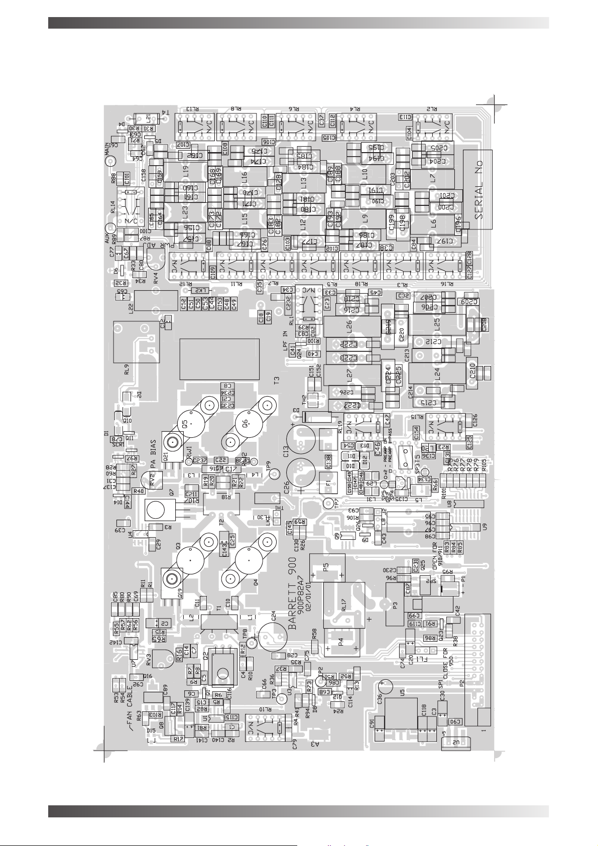
PA PCB overlay
BARRETT 900 SERIES TRANSCEIVERS
PAGE 87
Page 88

This page has been intentionally left blank
BARRETT 900 SERIES TRANSCEIVERS
PAGE 88
Page 89

PA schematic
See File: PA-SCHEMATIC.pdf
BARRETT 900 SERIES TRANSCEIVERS
PAGE 89
Page 90

This page has been intentionally left blank
BARRETT 900 SERIES TRANSCEIVERS
PAGE 90
Page 91

BARRETT 900 SERIES TRANSCEIVERS
BARRETT 900 PA BOARD PARTS LIST
---------------------------------------------------------------------------------------------------------------------------------------PCB P/N: PC-900P82A7 Issue A7 Sheet 1 of 8
Assembly P/N: SA-09935 STANDARD 900 PA
SA-09936 940 PA
---------------------------------------------------------------------------------------------------------------------------------------COMPONENT DESCRIPTION BARRETT COMMENTS
DESIGNATOR P/N
----------------------------------------------------------------------------------------------------------------------------------------
C1 CAP SMD 1206 0.1uF 5% 63V CP-00916
C2 CAP SMD TANTALUM 10uF 16V CP-01580
C3 CAP SMD TANTALUM 10uF 16V CP-01580
C4 CAP SMD 1206 0.1uF 5% 63V CP-00916
C5 CAP SMD 1206 0.1uF 5% 63V CP-0016
C6 CAP SMD 1206 0.1uF 5% 63V CP-00916
C7 CAP SMD 1206 0.1uF 5% 63V CP-00916
C8 CAP820pF mica CP-02134
C9 CAP 680pF SMD PHILIPS 2238-971-11547 CP-00068
C10 CAP SMD 1206 6n8 CERAMIC CP-00949
C11 CAP SMD 1206 6n8 CERAMIC CP-00949
C12 CAP SMD TANTALUM 1uF 16V CP-01570
C13 CAP ELECTRO RB 220uF 35V CP-01793
C14 CAP SMD 1206 0.1uF 5% 63V CP-00916
C15 CAP SMD 1206 0.1uF 5% 63V CP-00916
C16 CAP GREEN 3n9 100V CP-01505
C17 CAP GREEN 3n9 100V CP-01505
C18 CAP SMD 1206 0.1uF 5% 63V CP-00916
C19 CAP SMD 1206 0.1uF 5% 63V CP-00916
C20 CAP SMD TANTALUM 10uF 16V CP-01580
C21 CAP820pF mica CP-02134
C22 CAP 560pF SMD PHILIPS 2238-971-11546 CP-00067
C23 CAP SMD 1206 0.1uF 5% 63V CP-00916
C24 CAP ELECTRO RB 220uF 35V CP-01793
C25 CAP SMD 1206 0.1uF 5% 63V CP-00916
C26 CAP ELECTRO RB 220uF 35V CP-01793
C28 CAP SMD 1206 0.1uF 5% 63V CP-00916
C29 CAP SMD 1206 0.1uF 5% 63V CP-00916
C30 CAP SMD TANTALUM 10uF 16V CP-01580
C31 CAP SMD 1206 0.1uF 5% 63V CP-00916
C32 CAP SMD 1206 0.1uF 5% 63V CP-00916
C33 CAP SMD 1206 0.1uF 5% 63V CP-00916
C34 CAP SMD 1206 0.1uF 5% 63V CP-00916
C35 CAP SMD 1206 0.1uF 5% 63V CP-00916
C36 CAP ELECTRO RB 100uF 25V CP-11676
C37 CAP SMD 1206 0.1uF 5% 63V CP-00916
C38 CAP SMD 1206 0.1uF 5% 63V CP-00916
C39 CAP SMD 1206 0.1uF 5% 63V CP-00916
C40 CAP SMD 1206 0.1uF 5% 63V CP-00916
C41 CAP SMD 1206 0.1uF 5% 63V CP-00916
C42 CAP SMD 1206 0.1uF 5% 63V CP-00916
C43 CAP SMD 1206 0.1uF 5% 63V CP-00916
C44 CAP SMD TANTALUM 1uF 16V CP-01570
C45 CAP SMD 1206 0.1uF 5% 63V CP-00916
C46 CAP SMD 1206 0.1uF 5% 63V CP-00916
C47 CAP SMD 1206 0.1uF 5% 63V CP-00916
C48 CAP SMD 1206 1uF 10% 16V CP-00908
C49 CAP SMD 1206 1uF 10% 16V CP-00908
C50 CAP SMD 1206 0.1uF 5% 63V CP-00916
PAGE 91
Page 92

BARRETT 900 SERIES TRANSCEIVERS
BARRETT 900 PA BOARD PARTS LIST
---------------------------------------------------------------------------------------------------------------------------------------PCB P/N: PC-900P82A7 Issue A7 Sheet 2 of 8
Assembly P/N: SA-09935 STANDARD 900 PA
SA-09936 940 PA
---------------------------------------------------------------------------------------------------------------------------------------COMPONENT DESCRIPTION BARRETT COMMENTS
DESIGNATOR P/N
----------------------------------------------------------------------------------------------------------------------------------------
C51 CAP SMD 1206 0.1uF 5% 63V CP-00916
C52 CAP SMD 1206 0.1uF 5% 63V CP-00916
C53 CAP SMD 1206 1uF 10% 16V CP-00908
C54 CAP SMD 1206 0.1uF 5% 63V CP-00916
C61 CAP SMD 1206 0.1uF 5% 63V CP-00916
C62 CAP SMD 1206 0.1uF 5% 63V CP-00916
C63 CAP 390pF SMD PHILIPS 2238-971-11544 CP-00065
C64 CAP 39pF SMD PHILIPS 2238-971-11531 CP-00054
C65 CAP TANTALUM 1uF SMD 16V CP-01570
C66 CAP SMD 1206 0.1uF 5% 63V CP-0916
C67 CAP SMD 1206 0.1uF 5% 63V CP-00916
C68 CAP SMD 1206 0.1uF 5% 63V CP-00916
C69 CAP SMD 1206 0.1uF 5% 63V CP-00916
C74 CAP SMD 1206 0.1uF 5% 63V CP-00916
C75 CAP SMD 1206 0.1uF 5% 63V CP-00916
C76 CAP SMD 1206 0.1uF 5% 63V CP-00916
C77 CAP TANTALUM 1uF SMD 16V CP-01570
C78 CAP SMD 1206 0.1uF 5% 63V CP-00916
C79 CAP SMD 1206 0.1uF 5% 63V CP-00916
C80 CAP SMD 1206 0.1uF 5% 63V CP-00916
C82 CAP SMD 1206 0.1uF 5% 63V CP-00916
C83 CAP SMD 1206 0.1uF 5% 63V CP-00916
C84 CAP SMD 1206 0.1uF 5% 63V CP-00916
C85 CAP SMD 1206 0.1uF 5% 63V CP-00916
C86 CAP SMD 1206 0.1uF 5% 63V CP-00916
C87 CAP SMD 1206 0.1uF 5% 63V CP-00916
C88 CAP SMD 1206 0.1uF 5% 63V CP-00916
C89 CAP SMD 1206 0.1uF 5% 63V CP-00916
C90 CAP SMD 1206 0.1uF 5% 63V CP-00916
C91 CAP SMD TANTALUM 10uF 16V CP-01580
C92 CAP SMD 1206 0.1uF 5% 63V CP-00916
C93 CAP SMD 1206 0.1uF 5% 63V CP-00916
C95 CAP SMD 1206 0.1uF 5% 63V CP-00916
C96 CAP SMD 1206 0.1uF 5% 63V CP-00916
C97 CAP SMD 1206 0.1uF 5% 63V CP-00916
C98 CAP SMD 1206 0.1uF 5% 63V CP-00916
C99 CAP SMD 1206 0.1uF 5% 63V CP-00916
C100 CAP SMD 1206 0.1uF 5% 63V CP-00916
C101 CAP SMD 1206 0.1uF 5% 63V CP-00916
C102 CAP SMD 1206 0.1uF 5% 63V CP-00916
C103 CAP SMD 1206 0.1uF 5% 63V CP-00916
C104 CAP SMD 1206 0.1uF 5% 63V CP-00916
C105 CAP SMD 1206 0.1uF 5% 63V CP-00916
C106 CAP SMD 1206 0.1uF 5% 63V CP-00916
C107 CAP SMD 1206 0.1uF 5% 63V CP-00916
C108 CAP SMD 1206 0.1uF 5% 63V CP-00916
C109 CAP SMD 1206 0.1uF 5% 63V CP-00916
C110 CAP SMD 1206 0.1uF 5% 63V CP-00916
C111 CAP SMD 1206 0.1uF 5% 63V CP-00916
PAGE 92
Page 93

BARRETT 900 SERIES TRANSCEIVERS
BARRETT 900 PA BOARD PARTS LIST
---------------------------------------------------------------------------------------------------------------------------------------PCB P/N: PC-900P82A7 Issue A7 Sheet 3 of 8
Assembly P/N: SA-09935 STANDARD 900 PA
SA-09936 940 PA
---------------------------------------------------------------------------------------------------------------------------------------COMPONENT DESCRIPTION BARRETT COMMENTS
DESIGNATOR P/N
----------------------------------------------------------------------------------------------------------------------------------------
C112 CAP SMD 1206 0.1uF 5% 63V CP-00916
C113 CAP SMD 1206 0.1uF 5% 63V CP-00916
C114 CAP SMD TANTALUM 1uF 16V CP-01570
C115 CAP SMD 1206 0.1uF 5% 63V CP-00916
C116 CAP SMD 1206 0.1uF 5% 63V CP-00916
C117 CAP SMD 1206 0.1uF 5% 63V CP-00916
C118 CAP SMD TANTALUM 10uF 16V CP-01580
C119 CAP SMD 1206 0.1uF 5% 63V CP-00916
C125 CAP SMD 1206 0.1uF 5% 63V CP-00916
C126 CAP SMD 1206 0.1uF 5% 63V CP-00916
C127 CAP SMD 1206 0.1uF 5% 63V CP-00916
C128 CAP SMD 1206 0.1uF 5% 63V CP-00916
C130 CAP SMD 1206 0.1uF 5% 63V CP-00916
C131 CAP SMD 1206 0.1uF 5% 63V CP-00916
C134 CAP SMD 1206 0.1uF 5% 63V CP-00916
C135 CAP SMD 1206 0.1uF 5% 63V CP-00916
C136 CAP SMD 1206 0.1uF 5% 63V CP-00916
C137 CAP SMD 1206 2n2 5% 63V CP-00937
C138 CAP SMD 1206 470nF 5% 63V CP-00912
C139 CAP SMD TANTALUM 10uF 16V CP-01580
C140 CAP SMD 1206 0.1uF 5% 63V CP-00916
C141 CAP SMD 1206 0.1uF 5% 63V CP-00916
C142 CAP SMD 1206 0.1uF 5% 63V CP-00916
C143 CAP SMD TANTALUM 10uF 25V CP-01575
C144 CAP SMD 1206 0.1uF 5% 63V CP-00916
C145 CAP SMD 1206 0.1uF 5% 63V CP-00916
C146 CAP SMD 0805 1nF 5% 63V CP-00915
C147 CAP SMD 0805 560pF 5% 63V CP-00945
C148 CAP SMD 0805 120pF CP-00939
C149 CAP SMD 0805 120pF CP-00939
C150 CAP SMD 0805 1nF 5% 63V CP-00915
C151 CAP SMD 1206 0.1uF 5% 63V CP-00916
C152 CAP SMD 1206 0.1uF 5% 63V CP-00916
C153 CAP SMD 1206 1uF 10% 16V CP-00908
C154 CAP SMD 1206 0.1uF 5% 63V CP-00916
C156 CAP 27pF SMD PHILIPS 2238-971-11528 CP-00052
C157 CAP 12Pf SMD PHILIPS 2238-971-11524 CP-00049
C158 CAP 6.8pF SMD 500V 1206 CP-00047
C159 CAP 10 Pf SMD PHILIPS 2238-971-11523 CP-00048
C160 CAP 82pF SMD PHILIPS 2238-971-11535 CP-00058
C161 CAP 47pF SMD PHILIPS 2238-971-11532 CP-00055
C162 CAP 39pF SMD PHILIPS 2238-971-11531 CP-00054
C164 CAP 56pF SMD PHILIPS 2238-971-11533 CP-00056
C165 CAP 27pF SMD PHILIPS 2238-971-11528 CP-00052
C166 CAP 47pF SMD PHILIPS 2238-971-11532 CP-00055
C167 CAP 15Pf SMD PHILIPS 2238-971-11525 CP-00050
C168 CAP 12Pf SMD PHILIPS 2238-971-11524 CP-00049
C169 CAP 12Pf SMD PHILIPS 2238-971-11524 CP-00049
C170 CAP 180pF SMD PHILIPS 2238-971-11539 CP-00061
PAGE 93
Page 94

BARRETT 900 SERIES TRANSCEIVERS
BARRETT 900 PA BOARD PARTS LIST
---------------------------------------------------------------------------------------------------------------------------------------PCB P/N: PC-900P82A7 Issue A7 Sheet 4 of 8
Assembly P/N: SA-09935 STANDARD 900 PA
SA-09936 940 PA
---------------------------------------------------------------------------------------------------------------------------------------COMPONENT DESCRIPTION BARRETT COMMENTS
DESIGNATOR P/N
----------------------------------------------------------------------------------------------------------------------------------------
C171 CAP 15Pf SMD PHILIPS 2238-971-11525 CP-00050
C172 CAP 100pF SMD PHILIPS 2238-971-11536 CP-00059
C173 CAP 27pF SMD PHILIPS 2238-971-11528 CP-00052
C174 CAP 68pF SMD PHILIPS 2238-971-11534 CP-00057
C175 CAP 22Pf SMD PHILIPS 2238-971-11527 CP-00051
C177 CAP 100pF SMD PHILIPS 2238-971-11536 CP-00059
C178 CAP 39pF SMD PHILIPS 2238-971-11531 CP-00054
C180 CAP 270pF SMD PHILIPS 2238-971-11542 CP-00063
C181 CAP 39pF SMD PHILIPS 2238-971-11531 CP-00054
C182 CAP 100pF SMD PHILIPS 2238-971-11536 CP-00059
C183 CAP 100pF SMD PHILIPS 2238-971-11536 CP-00059
C184 CAP 82pF SMD PHILIPS 2238-971-11535 CP-00058
C185 CAP 82pF SMD PHILIPS 2238-971-11535 CP-00058
C186 CAP 150pF SMD PHILIPS 2238-971-11538 CP-00060
C187 CAP 6.8Pf SMD PHILIPS 2238-971-11523 CP-00047
C188 CAP 47pF SMD PHILIPS 2238-971-11532 CP-00055
C189 CAP 15Pf SMD PHILIPS 2238-971-11525 CP-00050
C190 CAP 470pF SMD PHILIPS 2238-971-11545 CP-00066
C191 CAP 12Pf SMD PHILIPS 2238-971-11524 CP-00049
C192 CAP 270pF SMD PHILIPS 2238-971-11542 CP-00063
C193 CAP 39pF SMD PHILIPS 2238-971-11531 CP-00054
C194 CAP 270pF SMD PHILIPS 2238-971-11542 CP-00063
C195 CAP 6.8pF SMD PHILIPS 2238-971-11523 CP-00047
C196 CAP 120pF SMD PHILIPS 2238-971-11538 CP-11661
C197 CAP 120pF SMD PHILIPS 2238-971-11538 CP-11661
C198 CAP 470pF SMD PHILIPS 2238-971-11545 CP-00066
C199 CAP 10 Pf SMD PHILIPS 2238-971-11523 CP-00048
C200 CAP 180pF SMD PHILIPS 2238-971-11539 CP-00061
C201 CAP 560pF SMD PHILIPS 2238-971-11546 CP-00067
C202 CAP 56pF SMD PHILIPS 2238-971-11533 CP-00056
C203 CAP 39pF SMD PHILIPS 2238-971-11531 CP-00054
C204 CAP 220pF SMD PHILIPS 2238-971-11541 CP-00062
C205 CAP 220pF SMD PHILIPS 2238-971-11541 CP-00062
C206 CAP 330pF SMD PHILIPS 2238-971-11543 CP-00064
C207 CAP 47pF SMD PHILIPS 2238-971-11532 CP-00055
C208 CAP 680pF SMD PHILIPS 2238-971-11547 CP-00068
C209 CAP 68pF SMD PHILIPS 2238-971-11534 CP-00057
C210 CAP 150pF SMD PHILIPS 2238-971-11538 CP-00060
C211 CAP SMD 1206 0.1uF 5% 63V CP-00916
C212 CAP 680pF SMD PHILIPS 2238-971-11547 CP-00068
C213 CAP 470pF SMD PHILIPS 2238-971-11545 CP-00066
C214 CAP 680pF SMD PHILIPS 2238-971-11547 CP-00068
C215 CAP 33pF SMD PHILIPS 2238-971-11529 CP-00053
C216 CAP 560pF SMD PHILIPS 2238-971-11546 CP-00067
C218 CAP 22Pf SMD PHILIPS 2238-971-11527 CP-00051
C219 CAP 820pF SMD PHILIPS 2238-971-11548 CP-00069
C220 CAP 330pF SMD PHILIPS 2238-971-11543 CP-00064
C222 CAP1000pF SMD PHILIPS 2238-971-11549 CP-00071
C223 CAP 820pF SMD PHILIPS 2238-971-11548 CP-00069
PAGE 94
Page 95

BARRETT 900 SERIES TRANSCEIVERS
BARRETT 900 PA BOARD PARTS LIST
---------------------------------------------------------------------------------------------------------------------------------------PCB P/N: PC-900P82A7 Issue A7 Sheet 5 of 8
Assembly P/N: SA-09935 STANDARD 900 PA
SA-09936 940 PA
---------------------------------------------------------------------------------------------------------------------------------------COMPONENT DESCRIPTION BARRETT COMMENTS
DESIGNATOR P/N
----------------------------------------------------------------------------------------------------------------------------------------
C224 CAP 220pF SMD PHILIPS 2238-971-11541 CP-00062
C225 CAP 12pF SMD 500V 1206 CP-00049
C226 CAP 330pF SMD PHILIPS 2238-971-11543 CP-00064
C227 CAP 820pF SMD PHILIPS 2238-971-11548 CP-00069
C230 CAP SMD 1206 0.1uF 5% 63V CP-00916
C231 CAP SMD 1206 0.1uF 5% 63V CP-00916
C232 CAP 56pF SMD PHILIPS 2238-971-11533 CP-00056
C234 CAP SMD 1206 330pF 5% 63V CP-00160
C235 CAP SMD 1206 330pF 5% 63V CP-00160
C237 CAP SMD 1206 0.1uF 5% 63V CP-00916
C238 CAP SMD 1206 0.1uF 5% 63V CP-00916
D1 DIODE GF1A DI-03354
D2 DIODE GF1A DI-03354
D3 DIODE 1.5KE18 DI-03319
D4 DIODE SMD BAV70 DI-03316
D5 DIODE SMD BAV70 DI-03316
D6 DIODE SMD BAV70 DI-03316
D8 DIODE SMD BAV70 DI-03316
D9 DIODE SMD BAV70 DI-03316
D10 DIODE ULTRA FAST ES1B DI-03312
D11 DIODE ULTRA FAST ES1B DI-03312
D12 DIODE ULTRA FAST ES1B DI-03312
D13 DIODE ULTRA FAST ES1B DI-03312
D14 DIODE ZENER BZX84C15 DI-03320
D15 DIODE SMD BAV70 DI-03316
F1 FUSE 3.15A M205 FU-04801
FL1 MURATA FILTER M103 FI-07618
J2 PLUG 3PIN CN-14102
L1 CHOKE 33uH SMD IN-03607
L2 CHOKE 33uH SMD IN-03607
L3 CHOKE 6u8H SMD IN-15006
L4 CHOKE 6u8H SMD IN-15006
L5 CHOKE SMD 1mH SMD IN-03585
L6 COIL 0.8uH 12 TURN 3000A CORE IN-13071
L7 COIL 1.44uH 17 TURN 3000A CORE IN-03105
L8 CHOKE 50uH NOT FITTED
L9 COIL 0.52uH 9 TURN 3000A CORE IN-03126
L10 COIL 0.936uH 13 TURN 3000A CORE IN-03107
L12 COIL 0.33uH 8 TURN 3000A CORE IN-13111
L13 COIL 0.6uH 11 TURN 3000M CORE IN-03109
L15 COIL 0.21uH 6 TURN 3000M CORE IN-03125
L16 COIL 0.378uH 9 TURN 3000M CORE IN-13109
L19 COIL 0.252uH 7 TURN 3000M CORE IN-03111
L20 CHOKE 100uH SMD IN-03601
L21 PART OF TRANSFORMER T4
L22 CHOKE 10 TURN 3000D CORE IN-03118
L23 COIL 0.14uH 5 TURN 3000M CORE IN-03124
L24 COIL 2.25uH 20 TURN 3000B CORE IN-03127
L25 COIL 1.25uH 14 TURN 3000B CORE IN-03128
PAGE 95
Page 96

BARRETT 900 SERIES TRANSCEIVERS
BARRETT 900 PA BOARD PARTS LIST
--------------------------------------------------------------------------------------------------------------------------------------PCB P/N: PC-900P82A7 Issue A7 Sheet 6 of 8
Assembly P/N: SA-09935 STANDARD 900 PA
SA-09936 940 PA
--------------------------------------------------------------------------------------------------------------------------------------COMPONENT DESCRIPTION BARRETT COMMENTS
DESIGNATOR P/N
---------------------------------------------------------------------------------------------------------------------------------------
L26 COIL 1.94uH 18 TURN 3000B CORE IN-03129
L27 COIL 3.49uH 24 TURN 3000B CORE IN-03113
L29 CHOKE 5u6H SMD IN-03606
L30 CHOKE 6u8H SMD IN-15006
L31 CHOKE 5u6H SMD IN-03606
P2 CONN IDC SKT 26 WAY CN-24121
P3 CONNECTOR 2 PIN POLARISED CN-03950
Q1 TRANSISTOR BFR92 TR-02260
Q2 TRANSISTOR BD139 TR-02205
Q3 TRANSISTOR BLV11 TR-02224
Q4 TRANSISTOR BLV11 TR-02224
Q5 TRANSISTOR MRF455 TR-02225
Q6 TRANSISTOR MRF455 TR-02225
Q7 TRANSISTOR BD139 TR-02205
Q8 TRANSISTOR BCP53 TR-02285
Q9 FET IRF7404 TR-00001
Q10 TRANSISTOR SMD BC807 TR-02229
Q11 TRANSISTOR SMD BC807 TR-02229
Q12 TRANSISTOR BC847 TR-02262
Q16 TRANSISTOR BCP53 TR-02285
Q19 TRANSISTOR BD139 TR-02205
Q21 TRANSISTOR 2N5192 TR-02212
Q22 FET 2SK125 TR-02245
Q23 FET SMD 2N7002 LT-1 TR-02282
Q24 TRANSISTOR BC847 TR-02262
Q25 TRANSISTOR BSP17 TR-02207
Q26 FET SMD 2N7002 LT-1 TR-02282
R1 RES SMD 1206 5% 220R RE-00119
R2 RES SMD 1206 5% 68R RE-00115
R3 RES SMD 1206 5% 330R RE-00107
R4 RES SMD 1206 5% 10R RE-00111
R5 RES SMD 1206 5% 3K3 RE-00127
R6 RES SMD 1206 5% 10K RE-00150
R7 RES SMD 1206 5% 3K3 RE-00127
R8 RES SMD 1206 5% 1K RE-00122
R9 RES SMD 1206 5% 47R RE-00113
R10 RES SMD 1206 5% 4R7 RE-00092
R11 RES SMD 1206 5% 220R RE-00119
R12 RES SMD 1206 5% 15R RE-00116
R13 RES SMD 1206 5% 1K RE-00122
R14 RES SMD 1206 5% 100R RE-00117
R15 RES SMD 1206 5% 220R RE-00119
R16 RES SMD 1206 5% 39R RE-00109
R17 RES SMD 1206 5% 220R RE-00119
R18 RES SMD 1206 5% 47R RE-00113
R19 RES SMD 1206 5% 4R7 RE-00092
R20 RES SMD 1206 5% 4R7 RE-00092
R21 RES SMD 1206 5% 4R7 RE-00092
R22 RES SMD 1206 5% 4R7 RE-00092
PAGE 96
Page 97

BARRETT 900 SERIES TRANSCEIVERS
BARRETT 900 PA BOARD PARTS LIST
---------------------------------------------------------------------------------------------------------------------------------------PCB P/N: PC-900P82A7 Issue A7 Sheet 7 of 8
Assembly P/N: SA-09935 STANDARD 900 PA
SA-09936 940 PA
---------------------------------------------------------------------------------------------------------------------------------------COMPONENT DESCRIPTION BARRETT COMMENTS
DESIGNATOR P/N
----------------------------------------------------------------------------------------------------------------------------------------
R23 RES SMD 1206 5% 10R RE-00111
R24 RES SMD 1206 5% 5K6 RE-00129
R26 RES SMD 1206 5% 2K2 RE-00125
R27 RES SMD 1206 5% 10K RE-00150
R28 RES SMD 1206 5% 4K7 RE-00128
R30 RES 1/4 WATT 5% 100R RE-00237
R31 RES 1/4 WATT 5% 100R RE-00237
R32 RES SMD 1206 5% 180K RE-00173
R33 RES SMD 1206 5% 4K7 RE-00128
R34 RES SMD 1206 5% 1K RE-00122
R35 RES SMD 1206 5% 100K RE-00170
R36 RES SMD 1206 5% 1K RE-00122
R37 RES SMD 1206 5% 4K7 RE-00128
R38 RES SMD 1206 5% 10K RE-00150
R39 RES SMD 1206 5% 10R RE-00111
R40 RES SMD 1206 5% 47R RE-00113
R41 RES SMD 1206 5% 1M RE-00178
R51 RES SMD 1206 5% 10K RE-00150
R52 RES SMD 1206 5% 3K3 RE-00127
R53 RES SMD 1206 5% 100K RE-00170
R54 RES SMD 1206 5% 100K RE-00170
R55 RES SMD 1206 5% 15K RE-00151
R56 RES SMD 1206 5% 15K RE-00151
R57 RES SMD 1206 5% 1K RE-00122
R58 RES SMD 1206 5% 1K5 RE-00124
R59 RES SMD 1206 5% 220R RE-00119
R60 RES SMD 1206 5% 1K RE-00122
R62 RES SMD 1206 5% 1K RE-00122
R63 RES SMD 1206 5% 120R RE-00095
R65 RES SMD 1206 5% 220R RE-00119
R66 RES SMD 1206 5% 68R RE-00115
R71 RES SMD 1206 5% 1K RE-00122
R73 RES SMD 1206 5% 100R RE-00117
R75 RES SMD 1206 5% 10R RE-00111
R76 RES SMD 1206 5% 10R RE-00111
R77 RES SMD 1206 5% 10R RE-00111
R78 RES SMD 1206 5% 10R RE-00111
R79 RES SMD 1206 5% 10R RE-00111
R80 RES SMD 1206 5% 10K RE-00150
R81 RES SMD 1206 5% 100R RE-00117
R82 RES SMD 1206 5% 220R RE-00119
R83 RES SMD 1206 5% 1K RE-00122
R84 RES SMD 1206 5% 1K RE-00122
R85 RES SMD 1206 5% 1K RE-00122
R86 RES SMD 1206 5% 1K RE-00122
R87 RES SMD 1206 5% 10R RE-00111
R88 RES SMD 1206 5% 100K RE-00170
R89 RES SMD 1206 5% 100K RE-00170
R90 RES SMD 1206 5% 10K RE-00150
PAGE 97
Page 98

BARRETT 900 SERIES TRANSCEIVERS
BARRETT 900 PA BOARD PARTS LIST
---------------------------------------------------------------------------------------------------------------------------------------PCB P/N: PC-900P82A7 Issue A7 Sheet 8 of 8
Assembly P/N: SA-09935 STANDARD 900 PA
SA-09936 940 PA
---------------------------------------------------------------------------------------------------------------------------------------COMPONENT DESCRIPTION BARRETT COMMENTS
DESIGNATOR P/N
----------------------------------------------------------------------------------------------------------------------------------------
R91 RES SMD 1206 5% 100R RE-00117
R94 RES SMD 1206 5% 6K8 RE-00130
R95 RES SMD 1206 5% 1K RE-00122
R96 RES SMD 1206 5% 1K8 RE-00133
R97 RES SMD 1206 5% 22K RE-00153
R100 RES SMD 1206 5% 2K2 RE-00125
R101 RES SMD 1206 5% 10R RE-00111
R103 RES SMD 1206 5% 100R RE-00117
R105 RES SMD 1206 5% 10R RE-00111
R106 RES SMD 1206 5% 2K2 RE-00125
R107 RES SMD 1206 5% 22R RE-00108
RL1 RELAY EA2-12 RL-05013
RL2 RELAY EA2-12 RL-05013
RL3 RELAY EA2-12 RL-05013
RL4 RELAY EA2-12 RL-0513
RL5 RELAY EA2-12 RL-05013
RL6 RELAY EA2-12 RL-05013
RL7 RELAY EA2-12 RL-05013
RL8 RELAY EA2-12 RL-05013
RL9 RELAY EP1-3L1S NEC RL-05020
RL10 RELAY EA2-12 RL-05013
RL11 RELAY EA2-12 RL-05013
RL12 RELAY EA2-12 RL-05013
RL13 RELAY EA2-12 RL-05013
RL14 RELAY EA2-12 RL-05013
RL15 RELAY EA2-12 RL-05013
RL16 RELAY EA2-12 RL-05013
RL17 RELAY EP1-3L1S NEC RL-05020
RL18 RELAY EA2-12 RL-05013
RL19 RELAY EA2-12 RL-05013
RV2 TRIMPOT 100R 5% IC-02511
RV3 TRIMPOT 100R 5% IC-02511
RV4 TRIMPOT CER 5K IC-02501
SCR1 THYRISTOR SMD P0102AL TY-02541
T1 TRANSFORMER P.A. 6/2+2 TURNS TF-03119
T2 TRANSFORMER P.A. 2+2+2 TURNS TF-03120
T3 OUTPUT TRANSFORMER FOR 900 SERIES TF-03121
T3 OUTPUT TRANSFORMER FOR 940 TF-94003
T4 TRANSFORMER P.A. 20+1 TURNS TF-30672
T5 TRANSFORMER P.A. 4+4+4 TURNS TF-03102
TH1 THERMISTOR TYPE P.T.C IC-02535
TH2OPTIONAL THERMAL SWITCH 57C IC-02552
U1 I/C MC1350 SMD8 IC-02709
U2OPTIONAL I/C 7805 T0220 IC-02316
U3 I/C LMC6042 SMD IC-02777
U4 I/C LM358 SMD IC-02706
U5 I/C LM2940S10 TO-263 IC-20002
U7 I/C LMC6042 SMD IC-02777
U8 I/C ULN2003 SMD IC-02717
U9 I/C 74HCT238 SMD IC-02798
PAGE 98
Page 99
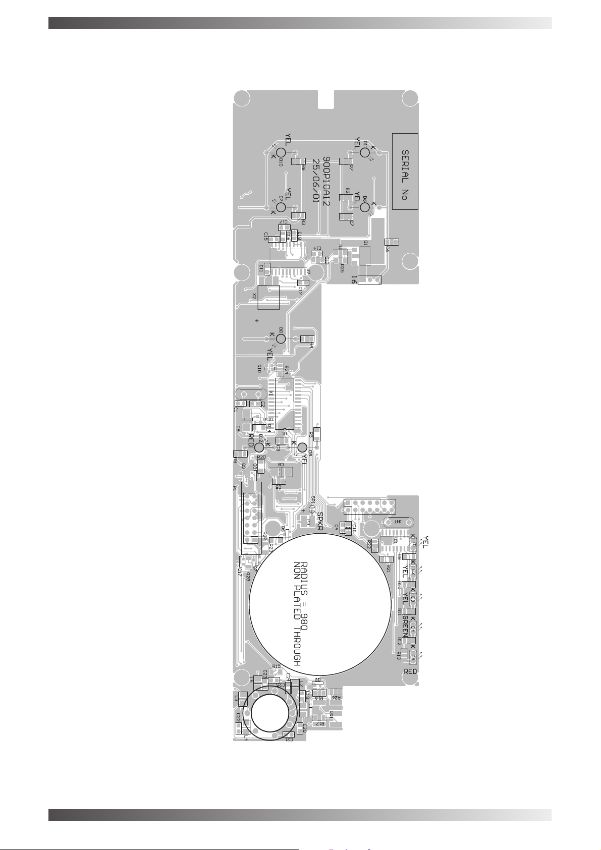
Front panel PCB overlay
BARRETT 900 SERIES TRANSCEIVERS
PAGE 99
Page 100
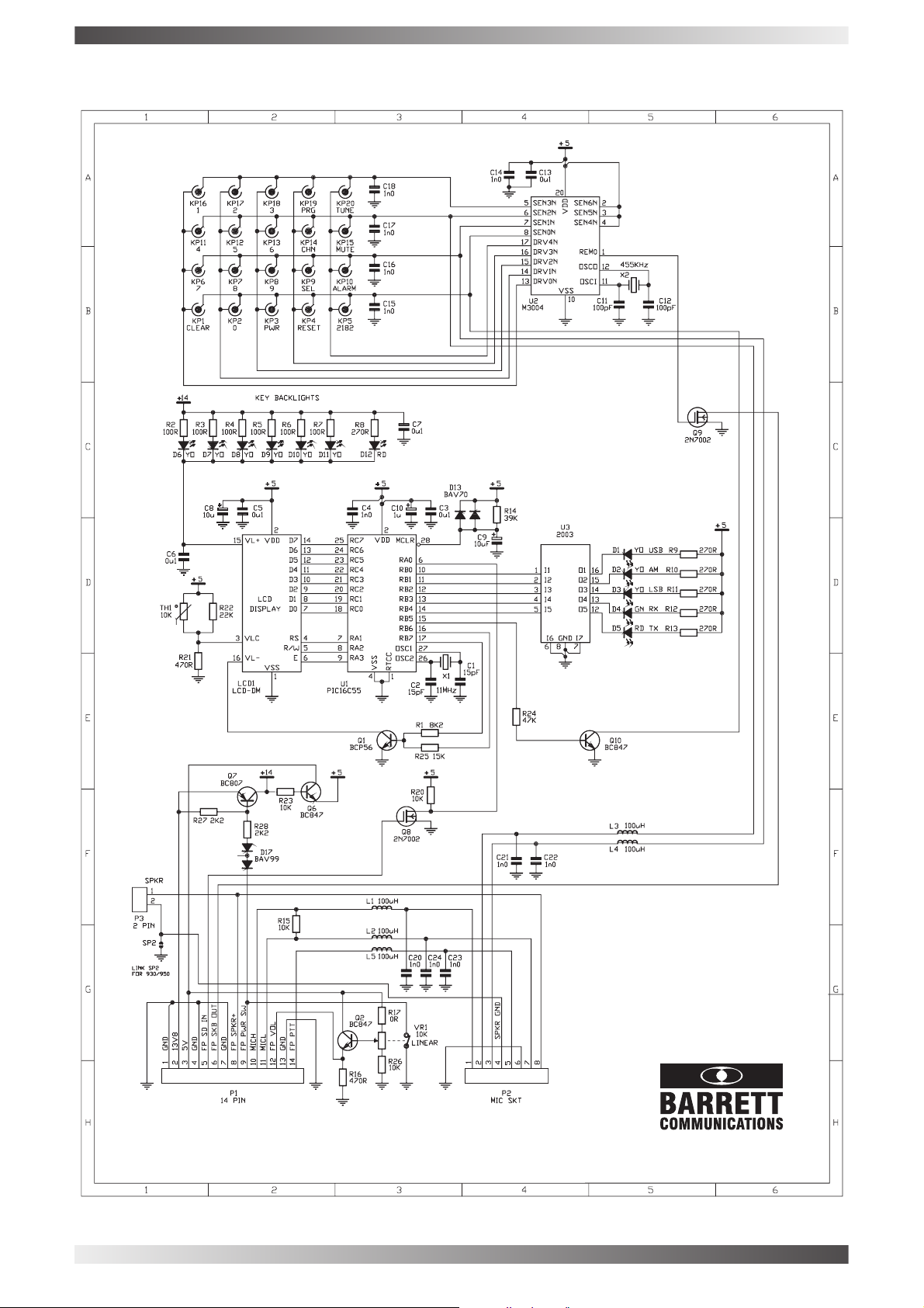
Front Panel Schematic
BARRETT 900 SERIES TRANSCEIVERS
PAGE 100
900 Front Panel Schematic
Drawing No: 900516A1
 Loading...