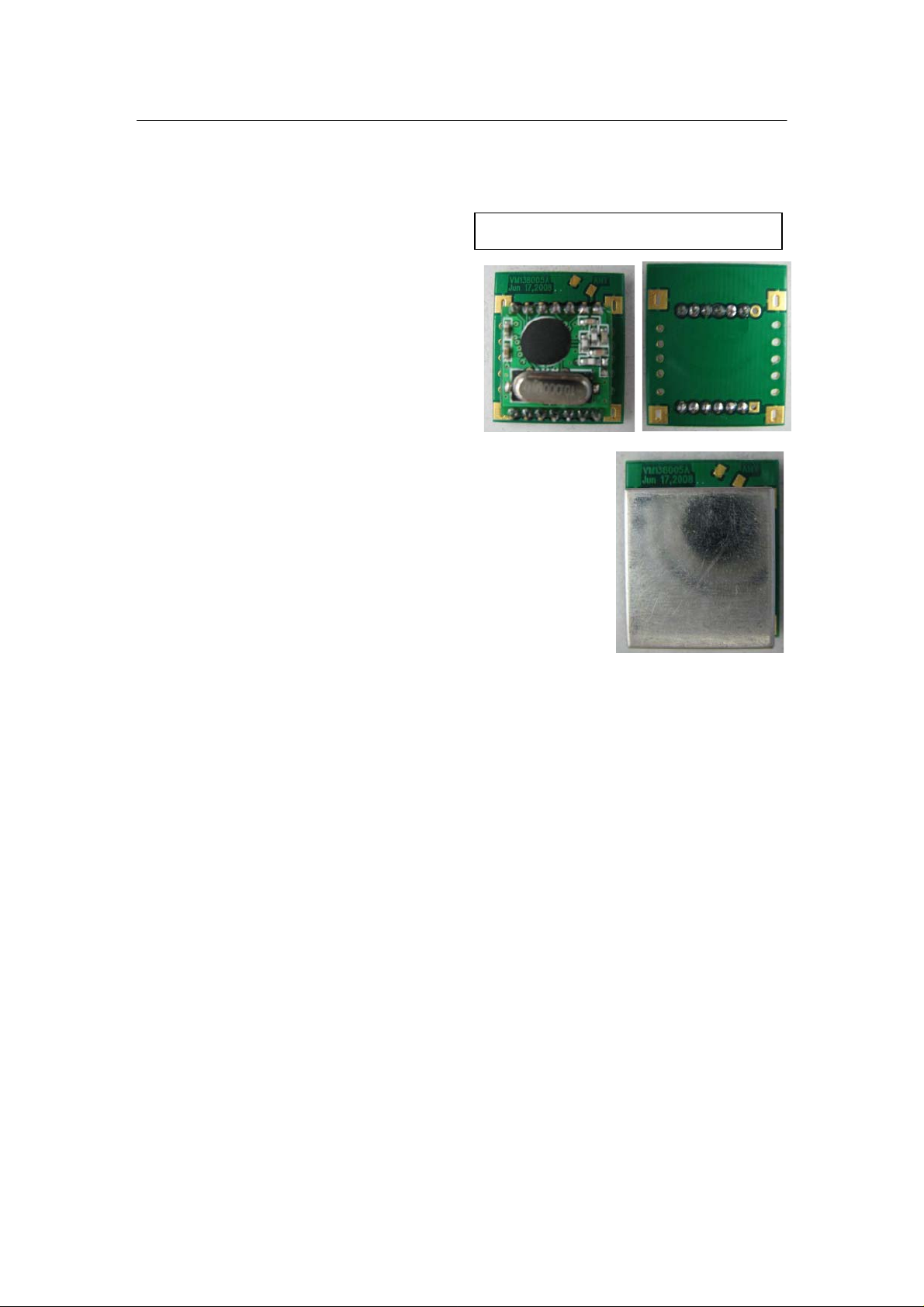
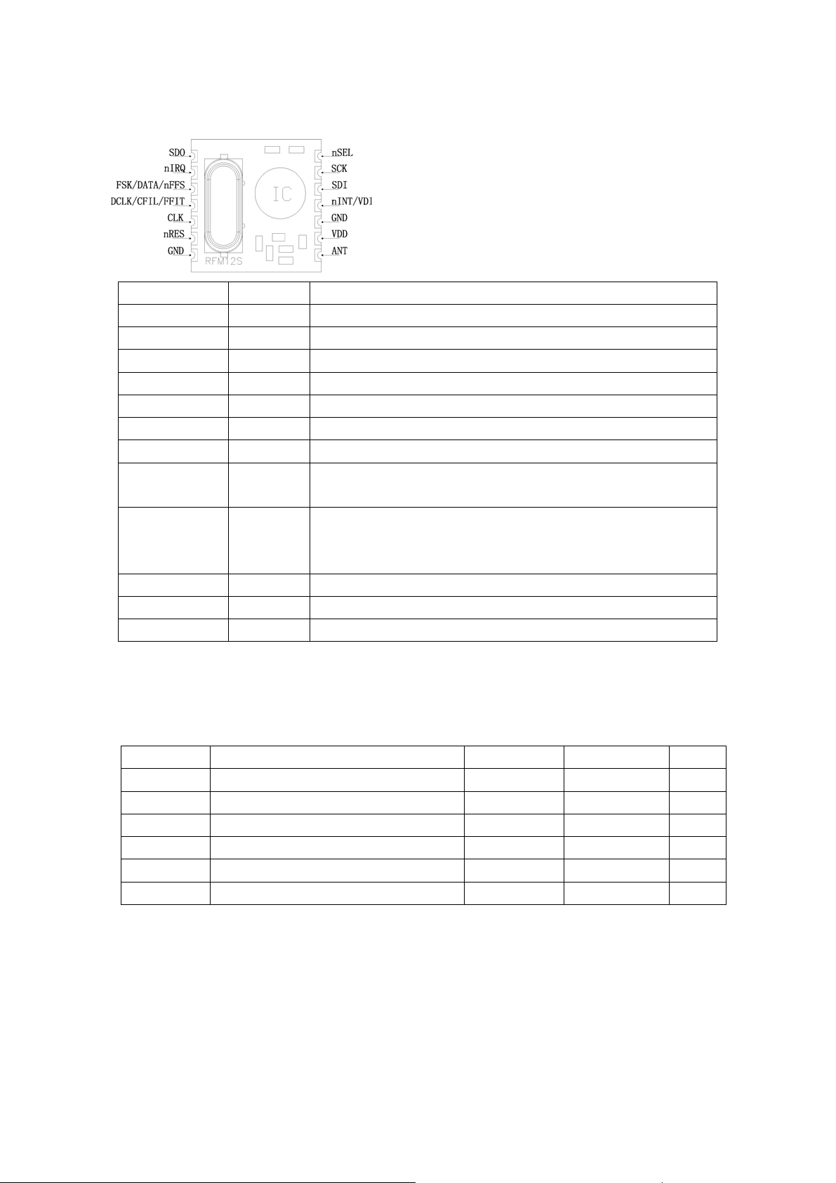
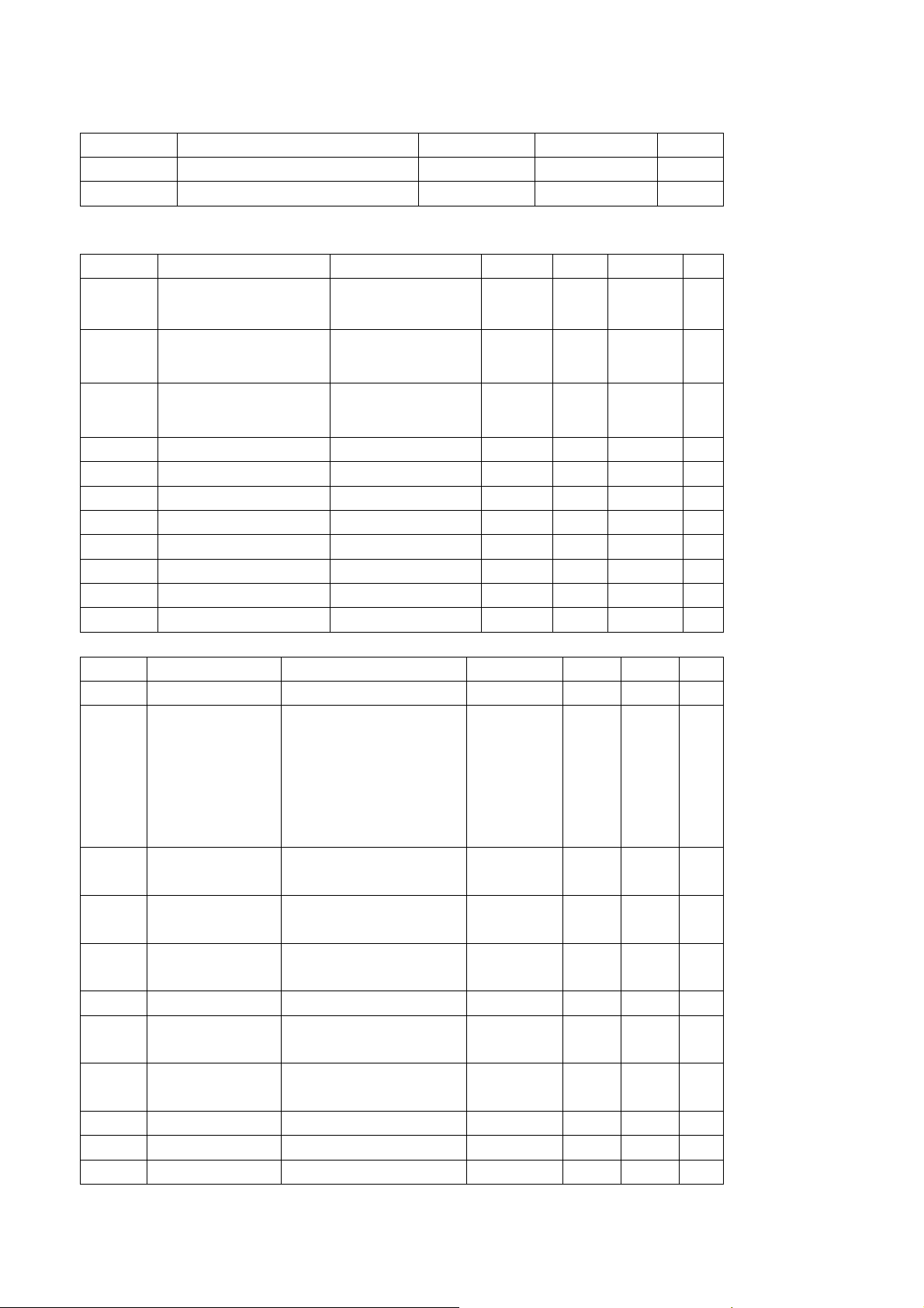
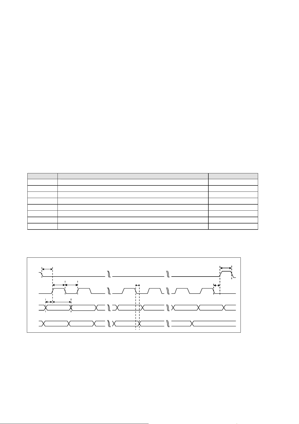
AZ Instrument VZ38915AZ User Manual

VZ38915AZ
UNIVERSAL ISM BAND FSK TRANSCEIVER
MODULE
General Introduction
VZ38915AZ is a low costing ISM band
transceiver module implemented with unique
PLL. The SPI interface is used to communicate
with microcontroller for parameter setting.
Features:
• Low costing, high performance and price ra tio
• Tuning free during production
• PLL and zero IF technology
• Fast PLL lock time
• Automatic antenna tuning
• Analog and digital signal strength indicator (ARSSI/DRSSI)
• Automatic frequency control (AFC)
• Data quality detection (DQD)
• Internal data filtering and clock recovery
• RX synchron pattern recognition
• SPI compatible serial control interface
• Clock and reset signal output for external MCU use
• 16 bit RX Data FIFO
• Two 8 bit TX data registers
• Standard 10 MHz crystal reference
• Wakeup timer
• 3.3V power supply
• Low power consumption
• Standby current less than 0.3uA
VZ38915AZ

“This device complies with Part 15 of the FCC Rules.
Operation is subject to the following two conditions: (1) this
device may not cause harmful interference, and (2) this device
must accept any interference received, including interference
that may cause undesired operation.”
“Changes or modifications not expressly approved by the
party responsible for compliance could void the user's
authority to operate the equipment.”

Pin Definition:
SMD
definition Type Function
nINT/VDI DI/ DO Interrupt input (active low)/Valid data indicator
VDD S Positive power supply
SDI DI SPI data input
SCK DI SPI clock input
nSEL DI Chip select (active low)
SDO DO Serial data output with bus hold
nIRQ DO
FSK/DATA/nFFS DI/DO/DI Transmit FSK data input/ Received data output (FIFO not used)/ FIFO
DCLK/CFIL/FFIT DO/AIO/DO Clock output (no FIFO )/ external filter capacitor(analog mode)/ FIFO
CLK DO Clock output for external microcontroller
nRES DIO
GND S Power ground
Interrupts request output(active low)
select
interrupts(active high)when FIFO level set to 1,
FIFO empty interruption can be achieved
Reset output(active low)
Electrical Parameter:
Maximum(not at working mode)
symbol parameter minimum maximum Unit
V
dd
V
in
Iin Input current except power -25 25 mA
ESD Human body model 1000 V
Tst Storage temperature -55 125 ℃
Tld Soldering temperature(10s) 260 ℃
Positive power supply -0.5 6.0 V
All pin input level -0.5 Vdd+0.5 V

Recommended working range
symbol parameter minimum maximum Unit
V
T
dd
op
Positive power supply 3.3*0.9 3.3*1.1 V
Working temperature -40 85
℃
DC characteristic
symbol parameter Remark minimum typical maximum Unit
I
dd_TX_0
I
dd_TX_PMAX
I
dd_RX
Supply current
(TX mode, P
Supply current
(TX mode, P
Supply current
= 0dBm)
out
= P
out
max
(RX mode)
I
Idle current Crystal oscillator on 0.62 1.2 mA
x
I
pd
V
il
V
ih
I
il
I
ih
V
ol
V
oh
Sleep mode current All blocks off 0.3 uA
Low level input 0.3*V
High level input 0.7*V
Leakage current Vil=0V -1 1 uA
Leakage current V
Low level output Iol=2mA 0.4 V
High level outp ut Ioh=-2mA Vdd-0.4 V
)
915MHz band
915MHz band
, V
ih=Vdd
=5.4V -1 1 uA
dd
17
24
13
V
dd
19
26
15
V
dd
AC characteristic
symbol parameter remark min typical max Unit
f
ref
BW Receiver
t
lock
tst, P
BR Data rate With internal digital
BR
A
P
min
AFC
RS
A
RS
R
C
ARSSI
PLL frequency 9 10 11 MHz
mode
0
bandwidth
PLL lock time After 10MHz step hopping,
mode
mode
mode
mode
mode
1
2
3
4
5
60
120
180
240
300
360
67
134
200
270
350
400
75
150
225
300
375
450
30 us
frequency error <10 kHz
PLL startup time
With a running crystal
oscillator
0.6 115.2 kbps
200
300 us
demodulator
Data rate With external RC filter 256 kbps
sensitivity BER 10
AFC working range df
range
BW=134KHz,BR=1.2kbps
received signal
-3
,
: FSK deviation in the
FSK
-102 -96 dBm
0.8*
df
FSK
RSSI accuracy ±5 dB
RSSI range 46 dB
ARSSI filter 1 nF
mA
mA
mA
KHz

RS
STEP
RS
RESP
RSSI
programmable step
DRSSI response
time
6 dB
RSSI output high after
valid , CARRSI=5nF
500 us
AC characteristic(Transmitter)
symbol parameter remark min typical max Unit
P
max_50
Max. output power delivered to
915MHZ band
5
dbm
50Ohm load over a suitable
915 MHz bands
7
dbm
P
max_ant
matching network
Max. EIRP with suitable selected
PCB antenna.
P
out
Typical output power Selectable in 3 dB
P
-21 P
max
max
dbm
steps
C
Output capacitance
o
(set by the automatic antenna
tuning circuit)
Q
o
Quality factor of the output
capacitance
L
BR
out
Output phase noise 100 kHz from carrier
FSK bit rate Via internal TX data
TX
In low bands
In high band s
In low bands
In high band s
1 MHz from carrier
2
2.1
13
8
2.6
2.7
15
10
3.2
pf
3.3
17
12
-80
dbc/HZ
-103
172 kbps
register
BRA
FSK bit rate
TX
df
fsk
TX data connected to the
FSK input
FSK frequency deviation Programmable in 15
256 kbps
15 240 kHZ
kHz steps
AC characteristic(Turn-on/Turnaround timings)
symbol parameter remark min typical max Unit
T
st
T
tx_XTAL_ON
T
rx_XTAL_ON
T
tx_rx_SYNT_ON
T
rx_tx_SYNT_ON
C
xl
Crystal oscillator startup
Crystal ESR < 100 1 5 ms
time
Transmitter turn-on
time
Receiver turn-on time Synthesizer off, crystal
Synthesizer off, crystal
oscillator on with 10 MHz step
oscillator on with 10 MHz step
Transmitter – Receiver
turnover time
Synthesizer and crystal
oscillator on during
TX/RX
Receiver – Transmit ter
turnover time
Synthesizer and crystal
oscillator on during
RX/TX
Crystal load
capacitance
Programmable in 0.5 pF steps,
tolerance+/- 10%
250
250
150
150
8.5 16 pf
us
us
us
us

t
POR
t
PBt
Internal POR timeout After V
final value
Wake-up timer clock
Calibrated every 30 seconds 0.96 1.05 ms
has reached 90% of
dd
100 ms
period
C
t
in, D
r, f
Digital input apacitance 2 pf
Digital output rise/fall
15pF pure capacitive load 10 ns
time

CONTROL INTERFACE
Commands to the transmitter are sent serially. Data bits on pin SDI are shifted into the device upon the rising edge of the clock
on
pin SCK whenever the chip select pin nSEL is low. When the nSEL signal is high, it initializes the serial
interface. All commands consist of a command code, followed by a varying number of parameter or data bits. All data are sent
MSB first (e.g. bit 15 for a 16bit command). Bits having no influence (don’t care) are indicated with X. The Power On Reset (POR) circuit sets default values
in all control and command registers.
The receiver will generate an interrupt request (IT) for the microcontroller - by pulling the nIRQ pin low - on the following events:
The TX register is ready to receive the next byte (RGIT)
The FIFO has received the preprogrammed amount of bits (FFIT)
Power-on reset (POR)
FIFO overflow (FFOV) / TX register underrun (RGUR)
Wake-up timer timeout (WKUP)
Negative pulse on the interrupt input pin nINT (EXT)
Supply voltage below the preprogrammed value is detected (LBD)
FFIT and FFOV are applicable when the FIFO is enabled. RGIT and RGUR are applicable only when the TX register is
enabled. To identify the source of the IT, the status bits should be read out.
Timing Specification
Symbol Parameter
t
C
t
C
t
S
t
S
t
S
t
D
t
D
t
O
Clock high time
Clock low time
Select setup time (nSEL falling edge to SCK rising edge)
Select hold time (SCK falling edge to nSEL rising edge)
Select high time
Data setup time (SDI transition to SCK rising edge)
Data hold time (SCK rising edge to SDI transition)
Data delay time
Minimum value [ns]
25
25
10
10
25
5
5
10
Timing Diagram
t
t
SS
nSEL
SCK
SDI
t
DS
tDH
t
BIT 15
CH
tCL
BIT 14
BIT 13
BIT 8
t
OD
BIT 7
BIT 1
BIT 0
SDO
FFIT
FFOV
CRL
AT S
OFFS(0)
FIFO OUT
SHI
t
SH
 Loading...