

Page 1

AudioMagic™ Module Datasheet
Point-to-Multipoint AVMD7211-04 Listener for
Wireless Audio Systems, based on Avnera’s AV7211 IC
General Description
Every consumer wants to be free from wires,
but system designers could never find a low-
cost, high-quality, easy-to-use wireless audio
solution for speakers, microphones,
headphones and headsets on the market.
Avnera’s proprietary wireless system changes
the game by taking a new approach to
wireless audio. The wireless protocol was
designed from the ground up and delivers
uncompressed stereo audio over the air
without interference problems.
Avnera’s wireless modules offer a low-touch,
easy-to-integrate wireless audio solution and
enable fast time to market by already solving
the problem associated with FCC, antenna
tuning and board optimization.
Modules based on Avnera’s AV72xx silicon
(also known as AudioMagic 1.5G) provide
breakthrough wireless audio functionality with
point to multipoint transport of uncompressed
stereo PCM audio data from a single
AVMD7211 sender and a total of up to three
simultaneous AVMD7212 listeners.
Applications
9 Wireless audio transmitter for portable
audio player
9 Wireless audio distribution hub for
surround speakers
Ordering Options
AVMD7211-04-ACNA: Analog-in, normal
range
AVMD7211-04-ACPA: Analog-in, extended
range
Features
9 Uncompressed audio, point to multipoint
capable (1 to 3)
9 Audio path SNR: Stereo 84 dB SNR, 48 kHz
sampling rate
9 Support for 14m (normal) and 30m
(extended) range
9 Frequency range: 2.4 GHz ISM band,
continuous dynamic frequency selection
9 Forward error correction coding, error
detection, and audio-specific error
concealment
9 Diversity antennas for multipath and fading
mitigation
9 Connector: Edge contact via array supports
surface mount
9 Auto-search/synch and dynamic channel
selection
9 Low, fixed latency suitable for video lip-
synch
9 Support for 16, 20, 24, and 32 bit PCM
words at 16, 22.05, 24, 32, 44.1, 48, and 96
kHz
9 General purpose over-the-air (OTA) serial
interface:
9 2 kbps, bi-directional, full duplex
9 Support for meta-data and remote
control commands
AVNERA CORPORATION | 16505 NW BETHANY COURT SUITE 100 | BEAVERTON, OREGON 97006, U.S.A. | MAIN +1.503.718.4100 | FAX +1.503.718.4101 | WWW.AVNERA.COM
AVNERA PROPRIETARY & CONFIDENTIAL | PROVIDED UNDER NDA
Page 2
AudioMagic AVMD7211-04 Module Datasheet PRELIMINARY v0p16
1 Table of Contents
General Description ______________________________________________________________ 1
Applications_____________________________________________________________________ 1
Ordering Options_________________________________________________________________ 1
Features________________________________________________________________________ 1
1 Table of Contents_____________________________________________________________ 2
2 Lists of Figures and Tables_____________________________________________________ 3
3 AVMD7211 Functional Block Diagrams__________________________________________4
4 AVMD7211 Pin Information ___________________________________________________ 6
5 AVMD7211 Mechanical Dimensions_____________________________________________7
6 Electrical Specifications _______________________________________________________ 8
6.1 Absolute Maximum Ratings _____________________________________________________________ 8
6.2 Recommended Operating Range__________________________________________________________ 8
6.3 Electrical Characteristics________________________________________________________________ 9
7 Application information ______________________________________________________ 10
7.1 Mechanical requirements_______________________________________________________________ 10
7.2 Application circuit ____________________________________________________________________ 14
7.3 EMI considerations____________________________________________________________________ 15
8 FCC and Industry Canada certification information _______________________________ 16
8.1 Label Information_____________________________________________________________________ 16
8.2 Equipment labeling requirements________________________________________________________ 16
8.3 User manual labeling requirements ______________________________________________________ 17
9 Ordering Information ________________________________________________________ 18
10 Contact Information and Legal Disclaimer _____________________________________ 19
CONTENTS SUBJECT TO CHANGE WITHOUT NOTICE 2 AVNERA PROPRIETARY & CONFIDENTIAL
Page 3
AudioMagic AVMD7211-04 Module Datasheet PRELIMINARY v0p16
2 Lists of Figures and Tables
Table 1: AVMD7211-04 Module Block Diagram Description______________________________________________ 5
Table 2: AVMD7211-04 Pin Information _____________________________________________________________ 6
Table 3; AVMD7211-04 Electrical Characteristics______________________________________________________ 9
Table 4: AVMD7211 Module Ordering Information ____________________________________________________ 18
Figure 1: AVMD7211 Module Block Diagram without RF Power Amplifier (normal range)............................................. 4
Figure 2: AVMD7211 Module Block Diagram with RF Power Amplifier (extended range)............................................... 4
Figure 3: AVMD7211 mechanical dimensions.................................................................................................................... 7
Figure 4: Main board ground plane guidelines in the vicinity of the module.................................................................... 10
Figure 5: Module mounting requirements on the main board...........................................................................................11
Figure 6: Keep out requirements around the antenna of the module................................................................................. 12
Figure 7: Enclosure spacing requirements around the antenna end of the module........................................................... 13
Figure 8: AVMD7211 application schematic.....................................................................................................................14
Figure 9: Example of sub-1GHz EMI suppression using in-line ferrite chips................................................................... 15
Figure 9: Module pictures (not shown actual size)............................................................................................................ 18
CONTENTS SUBJECT TO CHANGE WITHOUT NOTICE 3 AVNERA PROPRIETARY & CONFIDENTIAL
Page 4
AudioMagic AVMD7211-04 Module Datasheet PRELIMINARY v0p16
3 AVMD7211 Functional Block Diagrams
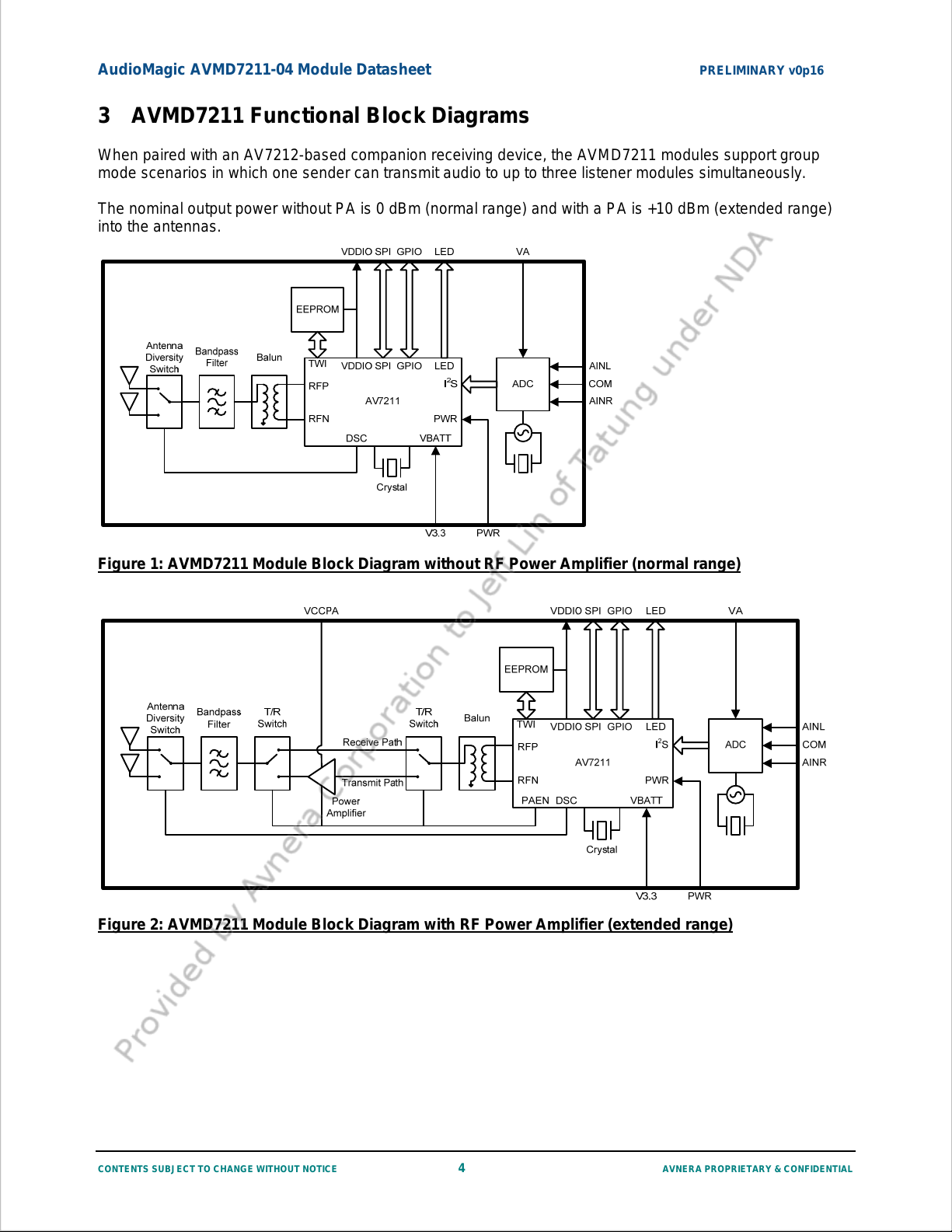
When paired with an AV7212-based companion receiving device, the AVMD7211 modules support group
mode scenarios in which one sender can transmit audio to up to three listener modules simultaneously.
The nominal output power without PA is 0 dBm (normal range) and with a PA is +10 dBm (extended range)
into the antennas.
Figure 1: AVMD7211 Module Block Diagram without RF Power Amplifier (normal range)
Figure 2: AVMD7211 Module Block Diagram with RF Power Amplifier (extended range)
CONTENTS SUBJECT TO CHANGE WITHOUT NOTICE 4 AVNERA PROPRIETARY & CONFIDENTIAL
Page 5
AudioMagic AVMD7211-04 Module Datasheet PRELIMINARY v0p16
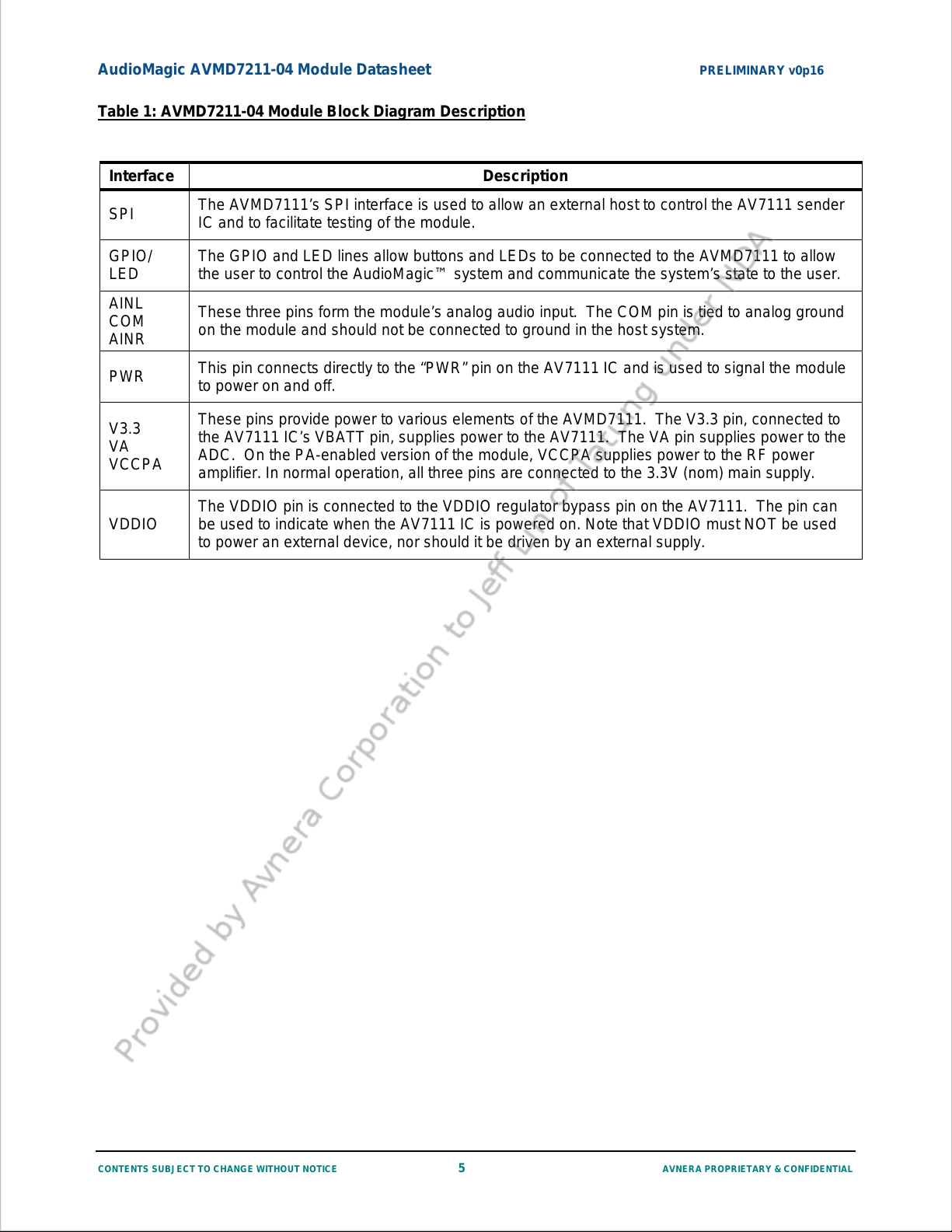
Table 1: AVMD7211-04 Module Block Diagram Description
Interface Description
SPI
GPIO/
LED
AINL
COM
AINR
PWR
V3.3
VA
VCCPA
VDDIO
The AVMD7111’s SPI interface is used to allow an external host to control the AV7111 sender
IC and to facilitate testing of the module.
The GPIO and LED lines allow buttons and LEDs to be connected to the AVMD7111 to allow
the user to control the AudioMagic™ system and communicate the system’s state to the user.
These three pins form the module’s analog audio input. The COM pin is tied to analog ground
on the module and should not be connected to ground in the host system.
This pin connects directly to the “PWR” pin on the AV7111 IC and is used to signal the module
to power on and off.
These pins provide power to various elements of the AVMD7111. The V3.3 pin, connected to
the AV7111 IC’s VBATT pin, supplies power to the AV7111. The VA pin supplies power to the
ADC. On the PA-enabled version of the module, VCCPA supplies power to the RF power
amplifier. In normal operation, all three pins are connected to the 3.3V (nom) main supply.
The VDDIO pin is connected to the VDDIO regulator bypass pin on the AV7111. The pin can
be used to indicate when the AV7111 IC is powered on. Note that VDDIO must NOT be used
to power an external device, nor should it be driven by an external supply.
CONTENTS SUBJECT TO CHANGE WITHOUT NOTICE 5 AVNERA PROPRIETARY & CONFIDENTIAL
Page 6
AudioMagic AVMD7211-04 Module Datasheet PRELIMINARY v0p16
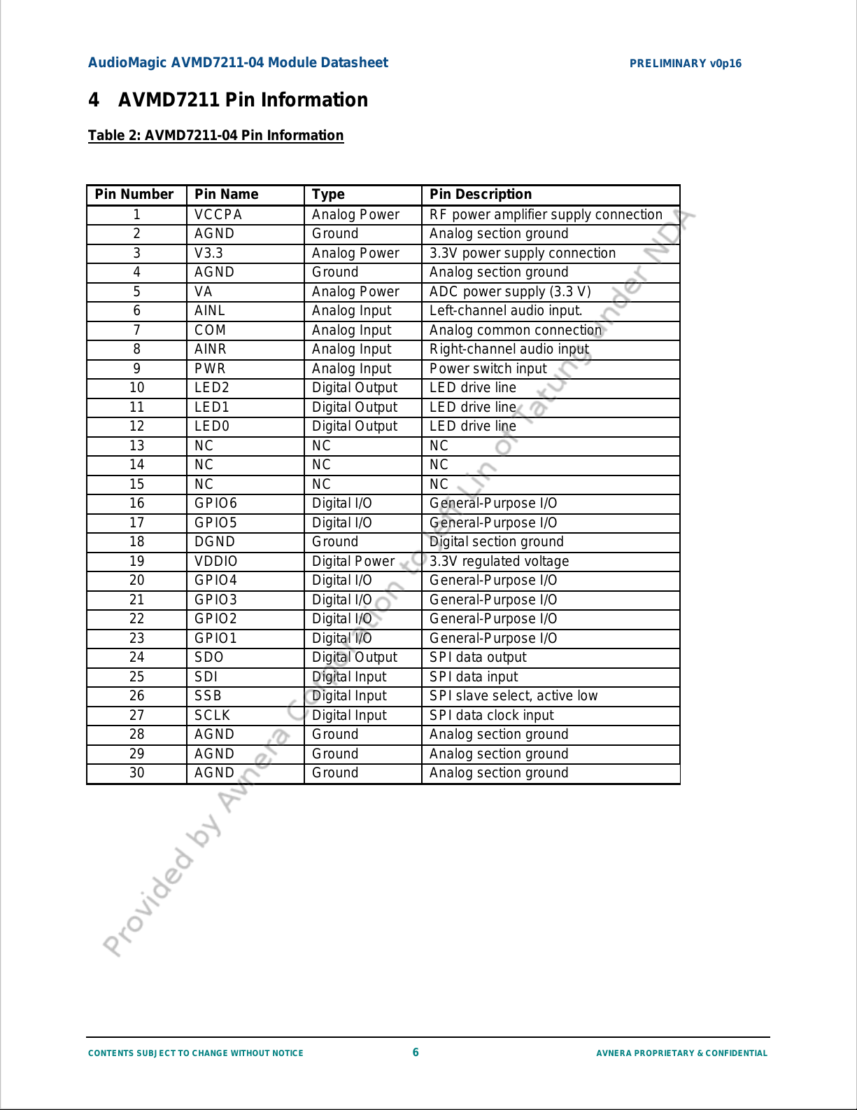
4 AVMD7211 Pin Information
Table 2: AVMD7211-04 Pin Information
Pin Number Pin Name Type Pin Description
1 VCCPA Analog Power RF power amplifier supply connection
2 AGND Ground Analog section ground
3 V3.3 Analog Power 3.3V power supply connection
4 AGND Ground Analog section ground
5 VA Analog Power ADC power supply (3.3 V)
6 AINL Analog Input Left-channel audio input.
7 COM Analog Input Analog common connection
8 AINR Analog Input Right-channel audio input
9 PWR Analog Input Power switch input
10 LED2 Digital Output LED drive line
11 LED1 Digital Output LED drive line
12 LED0 Digital Output LED drive line
13 NC NC NC
14 NC NC NC
15 NC NC NC
16 GPIO6 Digital I/O General-Purpose I/O
17 GPIO5 Digital I/O General-Purpose I/O
18 DGND Ground Digital section ground
19 VDDIO Digital Power 3.3V regulated voltage
20 GPIO4 Digital I/O General-Purpose I/O
21 GPIO3 Digital I/O General-Purpose I/O
22 GPIO2 Digital I/O General-Purpose I/O
23 GPIO1 Digital I/O General-Purpose I/O
24 SDO Digital Output SPI data output
25 SDI Digital Input SPI data input
26 SSB Digital Input SPI slave select, active low
27 SCLK Digital Input SPI data clock input
28 AGND Ground Analog section ground
29 AGND Ground Analog section ground
30 AGND Ground Analog section ground
CONTENTS SUBJECT TO CHANGE WITHOUT NOTICE 6 AVNERA PROPRIETARY & CONFIDENTIAL
Page 7
AudioMagic AVMD7211-04 Module Datasheet PRELIMINARY v0p16
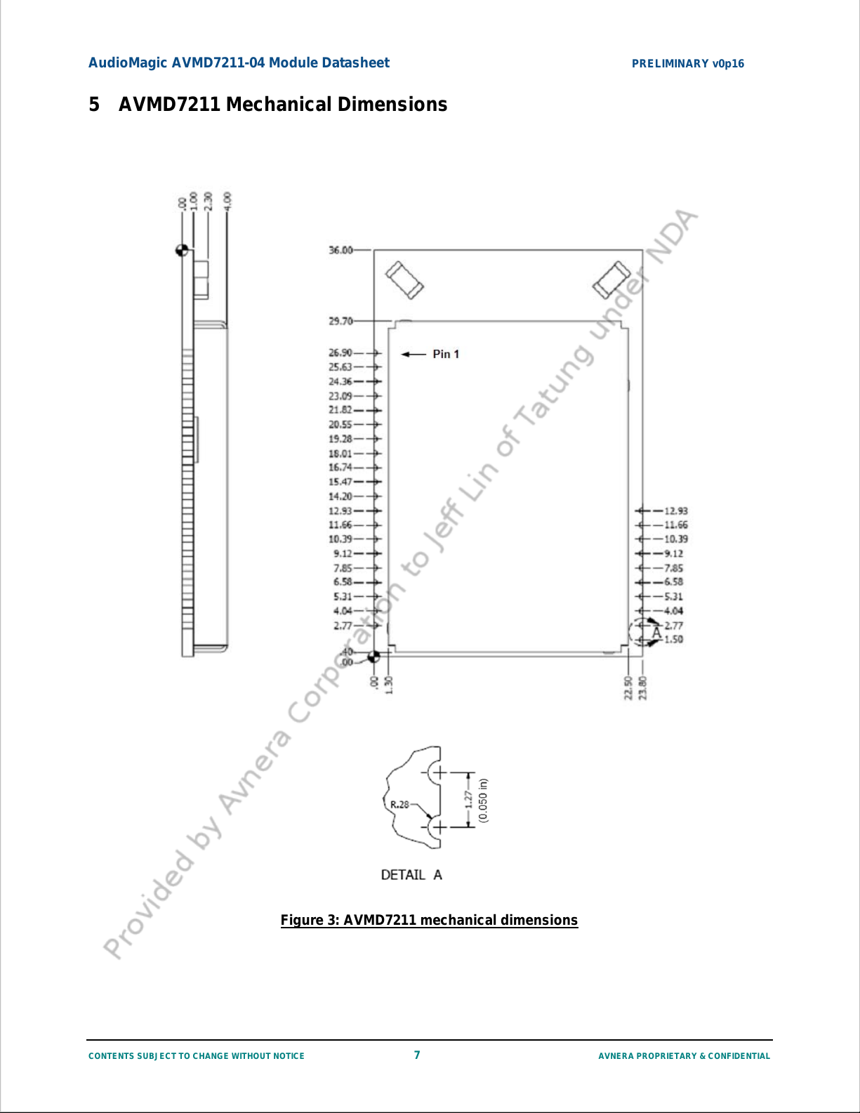
5 AVMD7211 Mechanical Dimensions
Figure 3: AVMD7211 mechanical dimensions
CONTENTS SUBJECT TO CHANGE WITHOUT NOTICE 7 AVNERA PROPRIETARY & CONFIDENTIAL
Page 8
AudioMagic AVMD7211-04 Module Datasheet PRELIMINARY v0p16
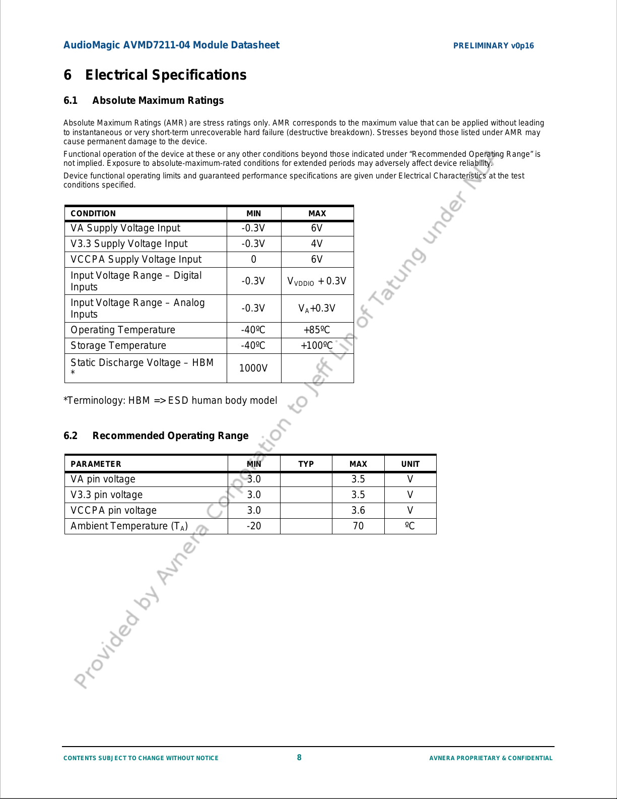
6 Electrical Specifications
6.1 Absolute Maximum Ratings
Absolute Maximum Ratings (AMR) are stress ratings only. AMR corresponds to the maximum value that can be applied without leading
to instantaneous or very short-term unrecoverable hard failure (destructive breakdown). Stresses beyond those listed under AMR may
cause permanent damage to the device.
Functional operation of the device at these or any other conditions beyond those indicated under “Recommended Operating Range” is
not implied. Exposure to absolute-maximum-rated conditions for extended periods may adversely affect device reliability.
Device functional operating limits and guaranteed performance specifications are given under Electrical Characteristics at the test
conditions specified.
CONDITION MIN MAX
VA Supply Voltage Input -0.3V 6V
V3.3 Supply Voltage Input -0.3V 4V
VCCPA Supply Voltage Input 0 6V
Input Voltage Range – Digital
Inputs
Input Voltage Range – Analog
Inputs
-0.3V V
-0.3V V
Operating Temperature -40ºC +85ºC
Storage Temperature -40ºC +100ºC
Static Discharge Voltage – HBM
*
1000V
*Terminology: HBM => ESD human body model
VDDIO
A
+ 0.3V
+0.3V
6.2 Recommended Operating Range
PARAMETER MIN TYP MAX UNIT
VA pin voltage 3.0 3.5 V
V3.3 pin voltage 3.0 3.5 V
VCCPA pin voltage 3.0 3.6 V
Ambient Temperature (TA) -20 70 ºC
CONTENTS SUBJECT TO CHANGE WITHOUT NOTICE 8 AVNERA PROPRIETARY & CONFIDENTIAL
Page 9
AudioMagic AVMD7211-04 Module Datasheet PRELIMINARY v0p16
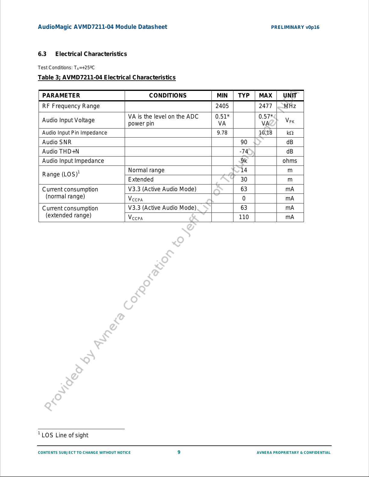
6.3 Electrical Characteristics
Test Conditions: TA=+25ºC
Table 3; AVMD7211-04 Electrical Characteristics
PARAMETER CONDITIONS MIN TYP MAX UNIT
RF Frequency Range 2405 2477 MHz
Audio Input Voltage
Audio Input Pin Impedance 9.78 10.18
VA is the level on the ADC
power pin
0.51*
VA
0.57*
VA
V
kΩ
PK
Audio SNR 90 dB
Audio THD+N -74 dB
Audio Input Impedance 9k ohms
Range (LOS)1
Normal range 14 m
Extended 30 m
Current consumption
(normal range)
Current consumption
(extended range)
V3.3 (Active Audio Mode) 63 mA
0 mA
V
CCPA
V3.3 (Active Audio Mode) 63 mA
110 mA
V
CCPA
1
LOS Line of sight
CONTENTS SUBJECT TO CHANGE WITHOUT NOTICE 9 AVNERA PROPRIETARY & CONFIDENTIAL
Page 10
AudioMagic AVMD7211-04 Module Datasheet PRELIMINARY v0p16
7 Application information
7.1 Mechanical requirements
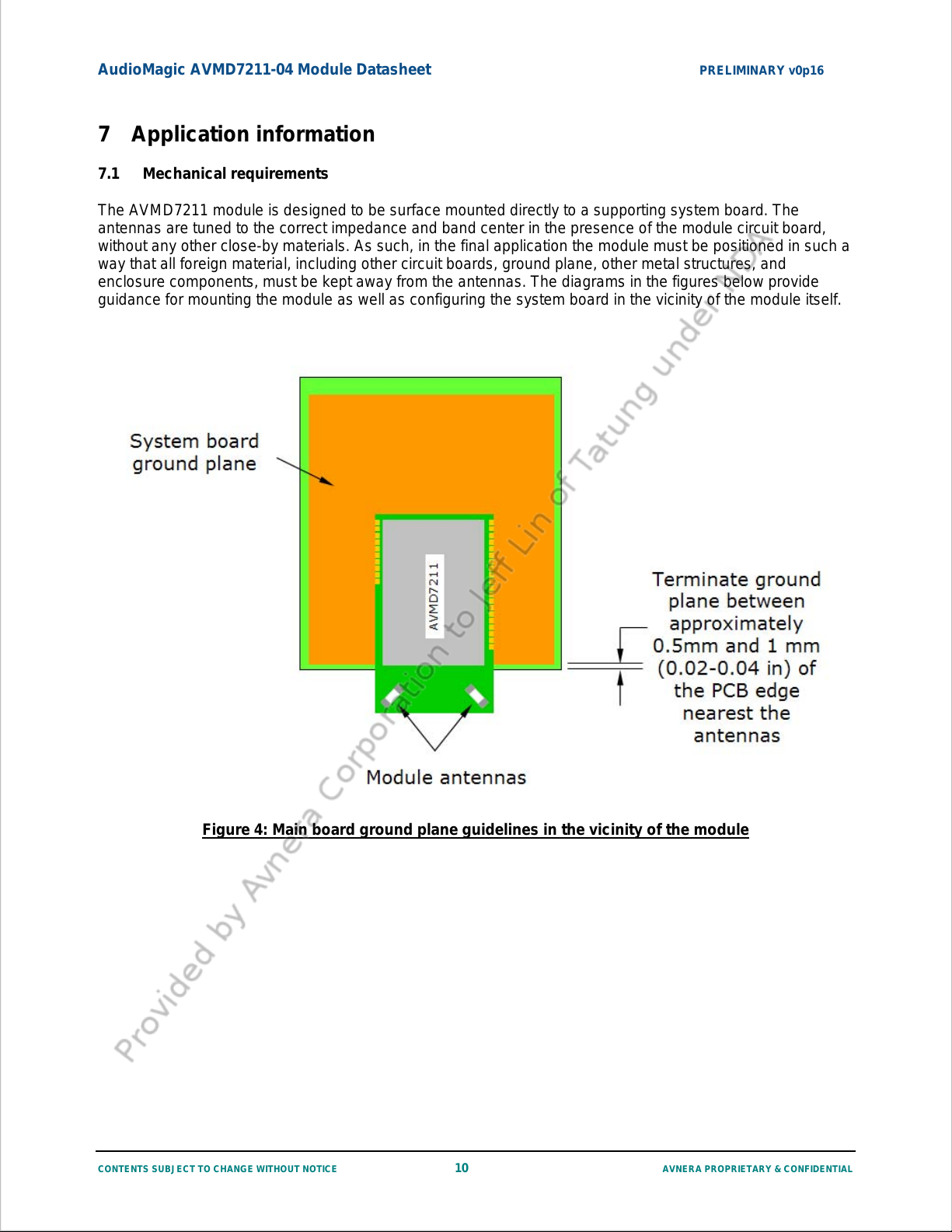
The AVMD7211 module is designed to be surface mounted directly to a suppo rting system board. The
antennas are tuned to the correct impedance and band center in the presence of the module circuit boa rd,
without any other close-by materials. As such, in the final application the module must be positioned in su ch a
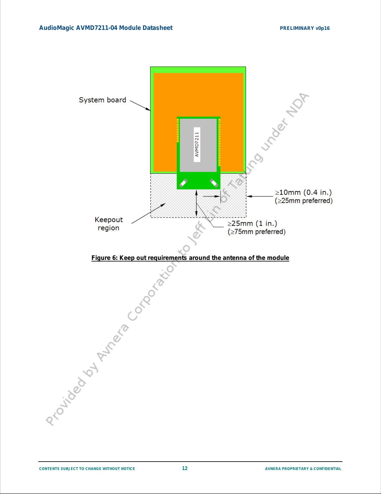
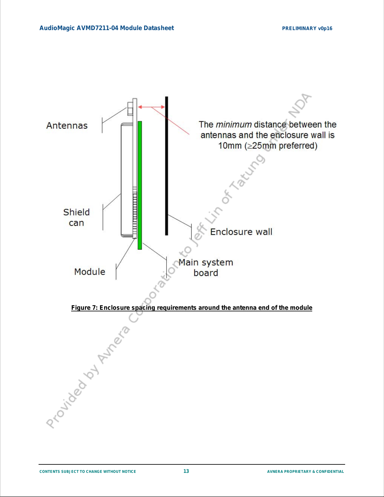
way that all foreign material, including other circuit boards, ground plane, other metal structures, and
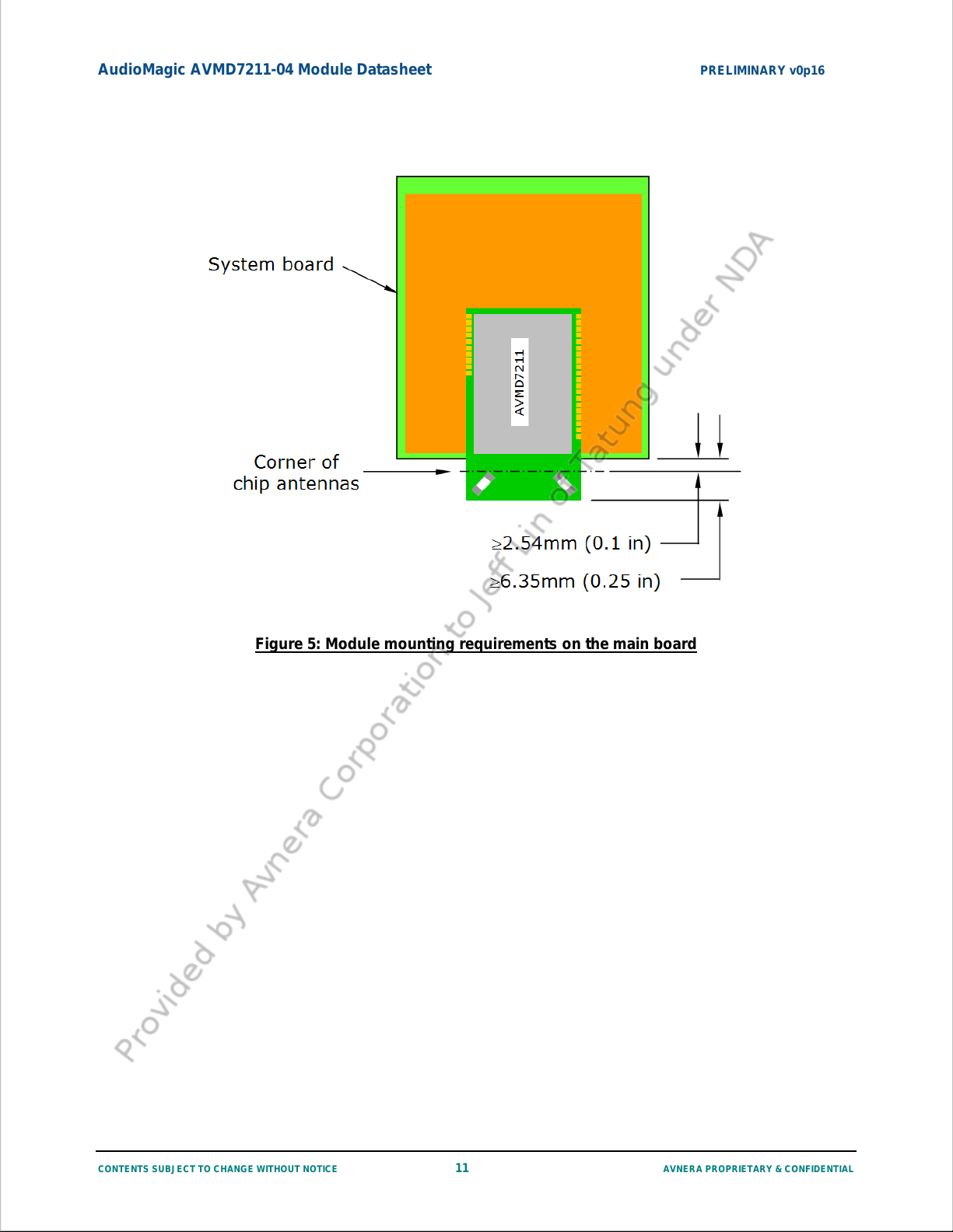
enclosure components, must be kept away from the antennas. The diagrams in the figures below provide
guidance for mounting the module as well as configuring the system board in the vicinity of the module itself.
Figure 4: Main board ground plane guidelines in the vicinity of the module
CONTENTS SUBJECT TO CHANGE WITHOUT NOTICE 10 AVNERA PROPRIETARY & CONFIDENTIAL
Page 11
AudioMagic AVMD7211-04 Module Datasheet PRELIMINARY v0p16
Figure 5: Module mounting requirements on the main board
CONTENTS SUBJECT TO CHANGE WITHOUT NOTICE 11 AVNERA PROPRIETARY & CONFIDENTIAL
Page 12
AudioMagic AVMD7211-04 Module Datasheet PRELIMINARY v0p16
Figure 6: Keep out requirements around the antenna of the module
CONTENTS SUBJECT TO CHANGE WITHOUT NOTICE 12 AVNERA PROPRIETARY & CONFIDENTIAL
Page 13
AudioMagic AVMD7211-04 Module Datasheet PRELIMINARY v0p16
Figure 7: Enclosure spacing requirements around the antenna end of the module
CONTENTS SUBJECT TO CHANGE WITHOUT NOTICE 13 AVNERA PROPRIETARY & CONFIDENTIAL
Page 14
AudioMagic AVMD7211-04 Module Datasheet PRELIMINARY v0p16
7.2 Application circuit
The schematic shown below represents a generic application, showing how the AVMD7212 would be
connected to the outside world for the purposes of control, power supply, and analog output.
TBD
Figure 8: AVMD7211 application schematic
CONTENTS SUBJECT TO CHANGE WITHOUT NOTICE 14 AVNERA PROPRIETARY & CONFIDENTIAL
Page 15
AudioMagic AVMD7211-04 Module Datasheet PRELIMINARY v0p16
7.3 EMI considerations
Applications employing long signal lines to connect to the module are under increased risk of EMI. This can
manifest as buzzing noise or spurious emissions impacting FCC certification. System designers should avoid:
• Long cables connecting the modules to headphones or spea kers
• Long power cords connecting the modules to AC wall adapters
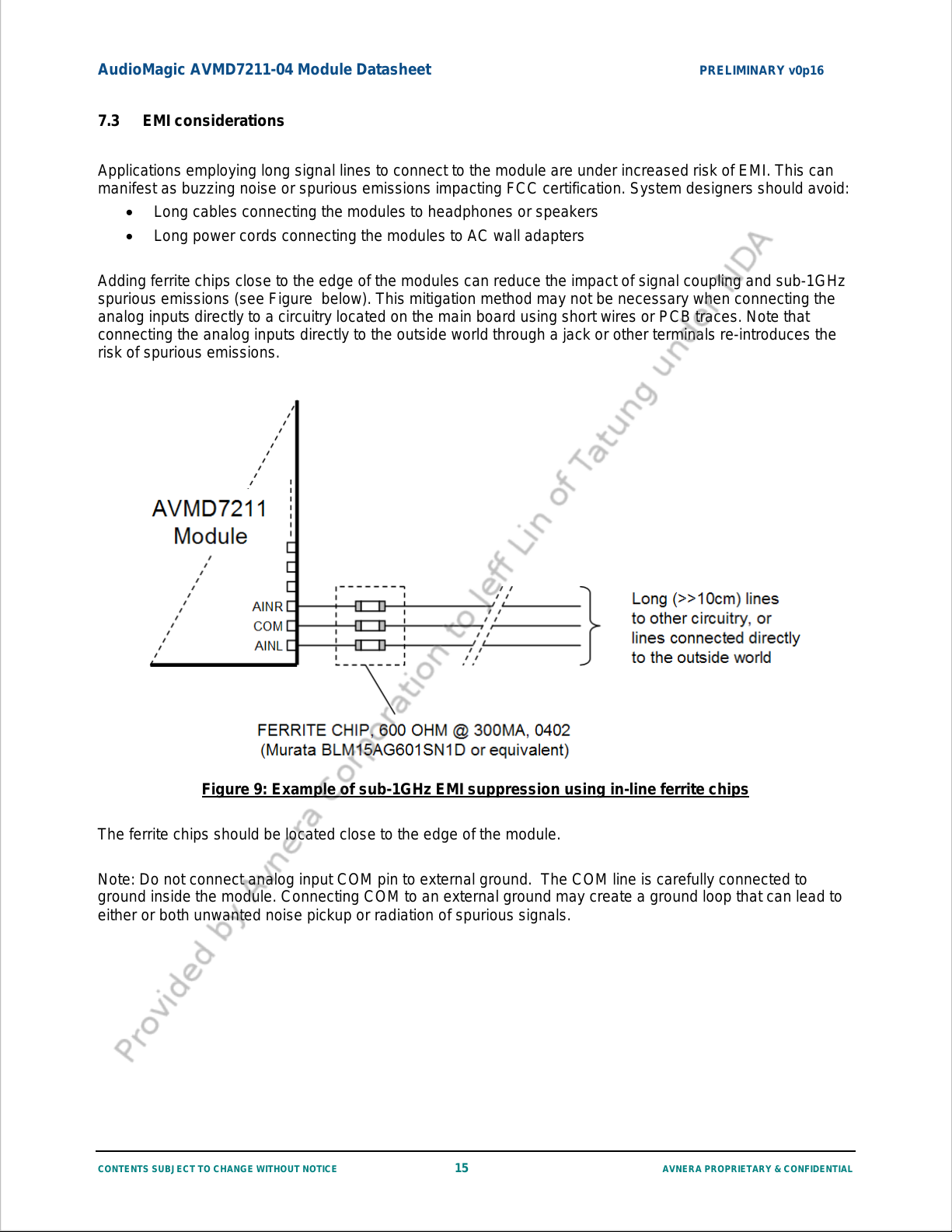
Adding ferrite chips close to the edge of the modules can reduce the impact of signal coupling and su b-1GHz
spurious emissions (see Figure below). This mitigation method may not be necessary when connecting the
analog inputs directly to a circuitry located on the main board using short wires or PCB traces. Note that
connecting the analog inputs directly to the outside world through a jack or other terminals re-introdu ces the
risk of spurious emissions.
Figure 9: Example of sub-1GHz EMI suppression using in-line ferrite chips
The ferrite chips should be located close to the edge of the module.
Note: Do not connect analog input COM pin to external ground. The COM line is carefully connected to
ground inside the module. Connecting COM to an external ground may create a ground loop that can lead to
either or both unwanted noise pickup or radiation of spurious signals.
CONTENTS SUBJECT TO CHANGE WITHOUT NOTICE 15 AVNERA PROPRIETARY & CONFIDENTIAL
Page 16
AudioMagic AVMD7211-04 Module Datasheet PRELIMINARY v0p16
8 FCC and Industry Canada certification information
8.1 Label Information
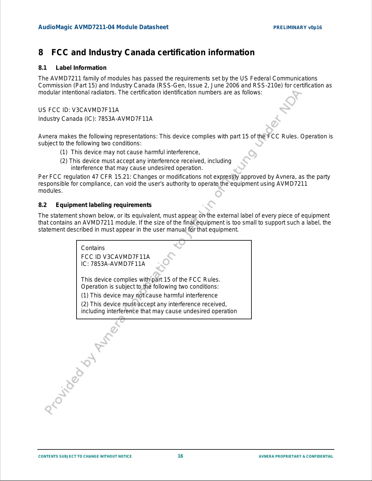
The AVMD7211 family of modules has passed the requirements set by the US Federal Communication s
Commission (Part 15) and Industry Canada (RSS-Gen, Issue 2, June 2006 and RSS-210e) for certification as
modular intentional radiators. The certification identification numbers are as follows:
US FCC ID: V3CAVMD7F11A
Industry Canada (IC): 7853A-AVMD7F11A
Avnera makes the following representations: This device complies with part 15 of the FCC Rules. Operation is
subject to the following two conditions:
(1) This device may not cause harmful interference,
(2) This device must accept any interference received, including
interference that may cause undesired operation.
Per FCC regulation 47 CFR 15.21: Changes or modifications not expressly approved by Avnera, as the party
responsible for compliance, can void the user’s authority to operate the equipment using AVMD7211
modules.
8.2 Equipment labeling requirements
The statement shown below, or its equivalent, must appear on the external label of every piece of equipment
that contains an AVMD7211 module. If the size of the final equipment is too small to support such a label, the
statement described in must appear in the user manual for that equipment.
Contains
FCC ID V3CAVMD7F11A
IC: 7853A-AVMD7F11A
This device complies with part 15 of the FCC Rules.
Operation is subject to the following two conditions:
(1) This device may not cause harmful interference
(2) This device must accept any interference received,
including interference that may cause undesired operation
CONTENTS SUBJECT TO CHANGE WITHOUT NOTICE 16 AVNERA PROPRIETARY & CONFIDENTIAL
Page 17
AudioMagic AVMD7211-04 Module Datasheet PRELIMINARY v0p16
8.3 User manual labeling requirements
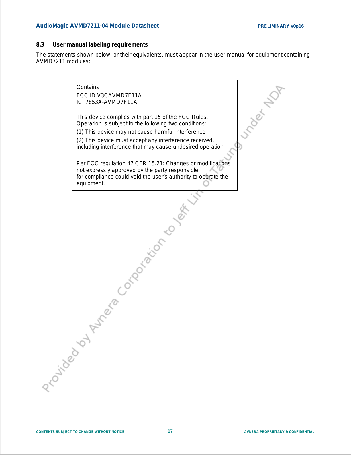
The statements shown below, or their equivalents, must appear in the user manual for equipment containing
AVMD7211 modules:
Contains
FCC ID V3CAVMD7F11A
IC: 7853A-AVMD7F11A
This device complies with part 15 of the FCC Rules.
Operation is subject to the following two conditions:
(1) This device may not cause harmful interference
(2) This device must accept any interference received,
including interference that may cause undesired operation
Per FCC regulation 47 CFR 15.21: Changes or modifications
not expressly approved by the party responsible
for compliance could void the user’s authority to operate the
equipment.
CONTENTS SUBJECT TO CHANGE WITHOUT NOTICE 17 AVNERA PROPRIETARY & CONFIDENTIAL
Page 18
AudioMagic AVMD7211-04 Module Datasheet PRELIMINARY v0p16
9 Ordering Information
Table 4: AVMD7211 Module Ordering Information
Module Part
Number
AVMD7211-04 ACNA Analog out, enables surface-mount, normal range,
AVMD7211-04 ACPA Analog out, enables surface-mount, extended range,
Option
Code
Description
integrated antennas
integrated antennas
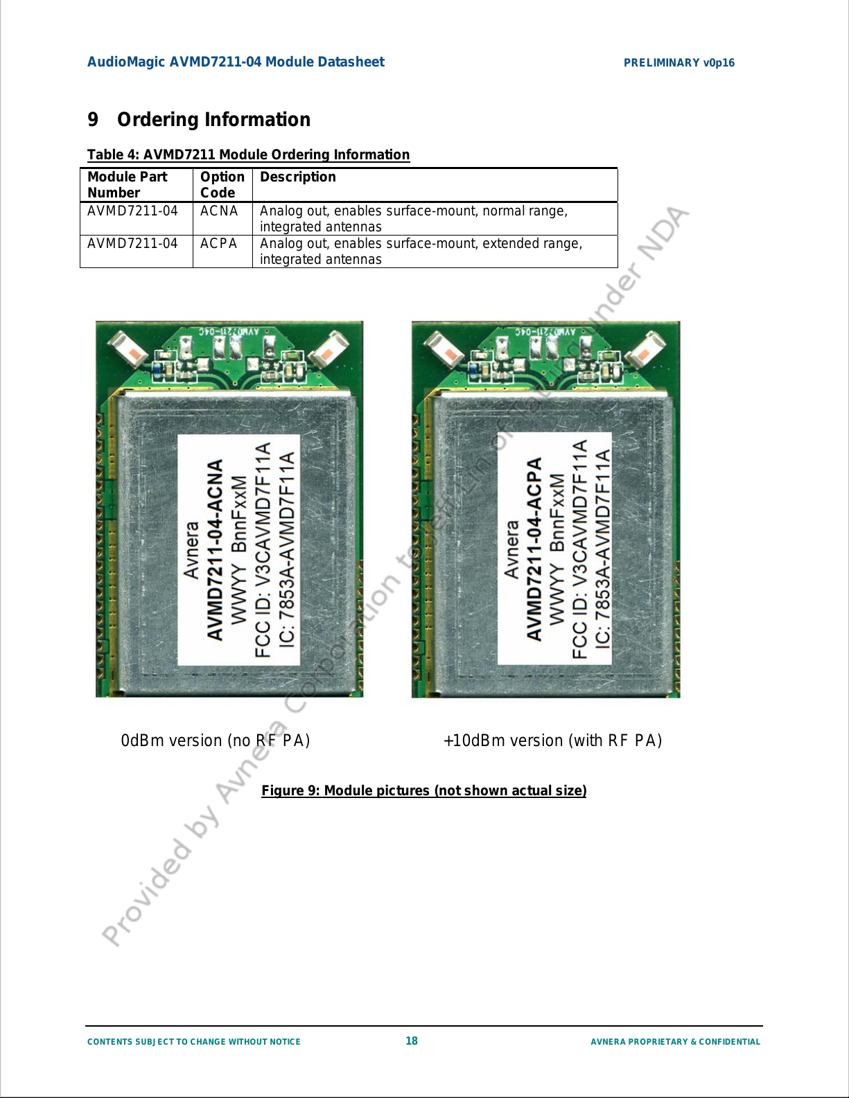
0dBm version (no RF PA) +10dBm version (with RF PA)
Figure 9: Module pictures (not shown actual size)
CONTENTS SUBJECT TO CHANGE WITHOUT NOTICE 18 AVNERA PROPRIETARY & CONFIDENTIAL
Page 19
AudioMagic AVMD7211-04 Module Datasheet PRELIMINARY v0p16
10 Contact Information and Legal Disclaimer
Avnera Corporation
16505 Bethany Court, Suite 100
Beaverton, Oregon 97006
U.S.A.
Main: +1.503.718.4100
Fax: +1.503.718.4101
www.avnera.com
Avnera Corporation reserves the right to make changes without notice to the product to improv e function,
reliability, or performance.
Avnera Corporation does not assume any liability arising from the application or use of the products or circuits
described herein.
CONTENTS SUBJECT TO CHANGE WITHOUT NOTICE 19 AVNERA PROPRIETARY & CONFIDENTIAL
 Loading...