

Page 1

PEX8605
1 Introduction
This document is intended for systems design engineers incorporating the PEX8605 PCI Express switch into a
system hardware design. It provides a handy list of basic design checks covering schematic and printed-circuit
board (PCB) layout designs. Including these checks as part of your design review can help insure that
important details are not overlooked when your design is committed to hardware, thereby improving your
chances for a successful bring-up. In preparation for your design review, we also recommend that you check
our website, www.plxtech.com, and download the most current technical specifications, errata, and related
documentation. This document supersedes and replaces previously dated versions.
2 Schematic Design Checks
This section includes checks on basic elements of the circuit design, including schematic symbol, power
supply, configuration straps, clocks, reset, configuration serial EEPROM, I2C, JTAG, GPIO, and other signals.
All power and signal pins on the device are covered.
2.1 Schematic Symbol
For designers using ORCAD schematic capture tools, an ORCAD symbol library is available on the PLX
website at www.plxtech.com. This library symbol is pre-checked by PLX engineers.
For designers not using the PLX-supplied schematic symbol, we highly recommend double-checking your
symbol’s signal pin names and numbers for accuracy before using the symbol in your schematic design.
2.2 Power Supply
2.2.1 Regulated DC Supply Voltages
The PEX8605 requires the following regulated DC voltages:
Core Logic Supply: 1.0 Volts (0.95V – 1.10V) – Powers core logic, SerDes Digital, and PLL
IO Supply: 2.5 or 3.3 Volts (2.3V – 3.6V) - Powers external I/O, SerDes Analog
2.2.2 Power Supply Sequencing Requirements
The Core Logic and IO supplies can be sequenced in any order. No special hardware is required to control the
order in which the power supply rails power up and down. It is recommended that both supplies be powered
up or down together.
© PLX Technology, www.plxtech.com Page 1 of 13 2 May 2013, version 1.7
Page 2
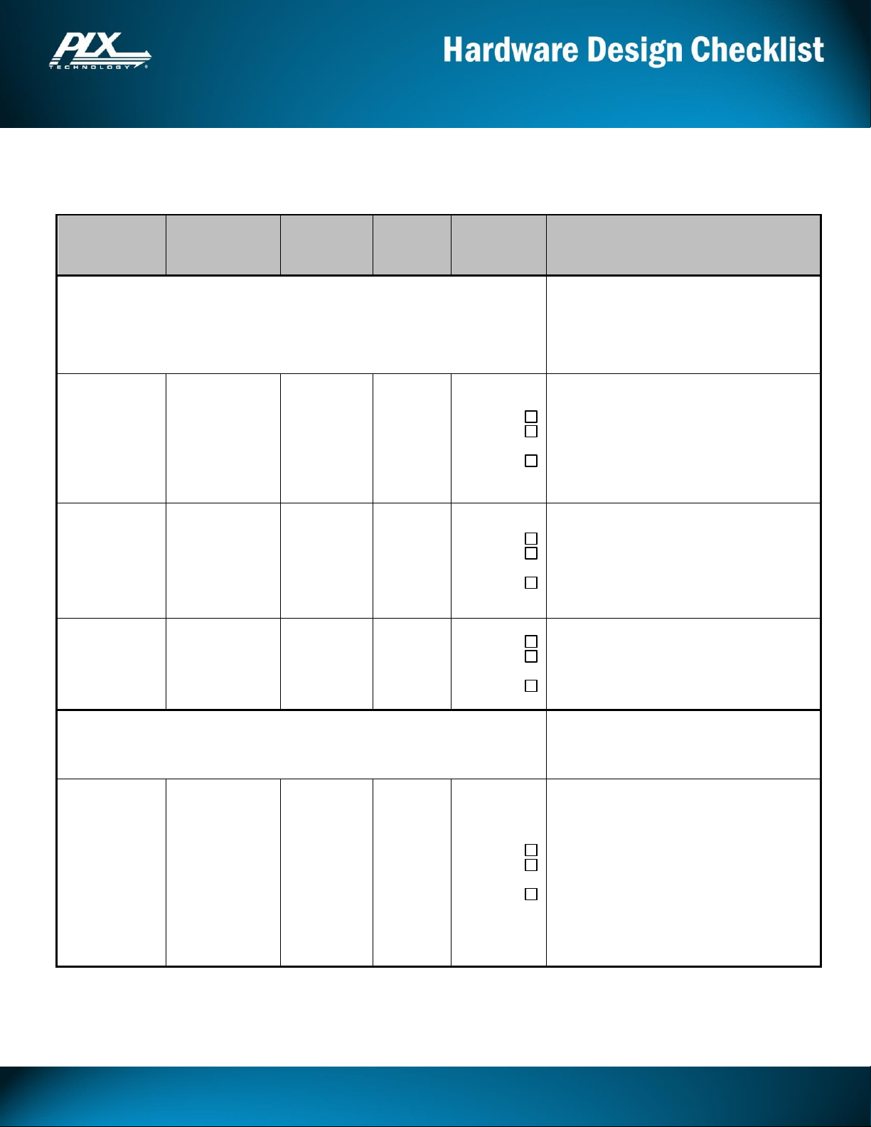
2.3 Power, Ground Pin Connections
Signal Name
Dual-Row
QFN Pkg.
Pin #
TQFP
Package
Pin #
Signal
Type
Checked
Recommendations
IO Power Pins (2.5 or 3.3 V)
In the simplest applications, all pins in this group
can be powered from a common 2.5 V or 3.3 V
DC voltage source. All pins in this group must be
at the same voltage. See the PEX8605 RDK
schematic for a reference circuit, including
recommended bypass cap network.PEX8605
PEX_VDDA_P0
PEX_VDDA_P1
PEX_VDDA_P2
PEX_VDDA_P3
B8
B13
B44
B50
14
26
101
114
APWR
YES
NO
UNKNOWN
Power for SerDes Analog Circuits (4 Pins)
Power for these pins should be filtered from the
main IO supply, VDD_IO. See the PEX8605
RDK schematic for a reference circuit.
Note: If stand-by power (D3cold) is implemented,
power for these pins should be filtered from the
auxiliary power supply, VAUX_IO.
VDD_IO
A30, A43, B3,
B31, B41
3, 4, 56, 70,
84, 92
IOPWR
YES
NO
UNKNOWN
Power for Digital IO Circuits (5 Pins)
Main supply for digital IO circuits.
Important Note: Data Sheet version 1.2 corrects
pins A26 and B19 as VAUX_IO. Designs
powering VDD_IO and VAUX_IO supplies
separately may be impacted by this change.
VAUX_IO
A18, A26, A64,
B19
33, 42, 49, 127
IOPWR
YES
NO
UNKNOWN
Auxiliary Power Supply (4 Pins)
If stand-by power is implemented, this power
supply should be derived from Vaux (3.3V).
Otherwise, connect these pins to the VDD_IO
supply.
Core Logic, SerDes, and PLL Power Pins
In the simplest applications, all 1.0 V supply pins
can be powered from a common 1.0 V DC voltage
source. See the PEX8605 RDK schematic for a
reference circuit.
PEX_VDDD0_P0
PEX_VDDD0_P1
PEX_VDDD0_P2
PEX_VDDD0_P3
PEX_VDDD1_P0
PEX_VDDD1_P1
PEX_VDDD1_P2
PEX_VDDD1_P3
B7
B12
B45
B51
A7
A13
B46
B52
12
24
103
116
9
21
106
119
DPWR
YES
NO
UNKNOWN
1.0 V Power for SerDes Digital Circuits (8
Pins)
Power for these pins should be filtered from the
main 1.0 V supply, VDD_CORE. See the PEX
8603 RDK schematic for a reference circuit.
Note: If stand-by power (D3cold) is implemented,
power for these pins should be filtered from the
auxiliary power 1.0V supply, VAUX_CORE.
PEX8605
© PLX Technology, www.plxtech.com Page 2 of 13 2 May 2013, version 1.7
Page 3
PEX8605
Signal Name
Dual-Row
QFN Pkg.
Pin #
TQFP
Package
Pin #
Signal
Type
Checked
Recommendations
PLL_AVDD
A31
58
PLLPWR
YES
NO
UNKNOWN
1.0 V Power for PLL Analog Circuits
This pin supplies power to the internal PLL. As
such it is sensitive to noise, and should be filtered
from the main 1.0V supply (VDD_CORE) to
reduce noise. See the RDK schematic for an
example filter circuit.
VDD_CORE
A29, A37, A46,
A50, B26, B43
54, 57, 72, 89,
98, 99
CPWR
YES
NO
UNKNOWN
1.0 V Power for Core Digital Logic (6 Pins)
Main 1.0 V supply for digital core logic.
VAUX_CORE
A10, A57, B49
15, 16, 112,
113
CPWR
YES
NO
UNKNOWN
1.0 V Auxiliary Core Logic Power Supply
(QFN: 3 Pins, TQFP: 4 pins)
If stand-by power is implemented, this power
supply should be regulated from Vaux (3.3V).
Otherwise, connect these pins to the VDD_CORE
supply.
Ground Pins (20 Pins and Center Pad)
Connect all Ground pins below directly to Ground
(plane).
PLL_AGND
B27
59
GND
YES
NO
UNKNOWN
Connect to Ground
PEX_VSSA_P0
PEX_VSSA_P1
PEX_VSSA_P2
PEX_VSSA_P3
A9
A15
A51
A58
13
25
102
115
GND
YES
NO
UNKNOWN
Connect to Ground (4 Pins)
PEX_VSSD0_P0
PEX_VSSD0_P1
PEX_VSSD0_P2
PEX_VSSD0_P3
PEX_VSSD1_P0
PEX_VSSD1_P1
PEX_VSSD1_P2
PEX_VSSD1_P3
B5
A12
A54
B53
B4
B9
B48
B54
8
20
107
120
5
17
110
123
GND
YES
NO
UNKNOWN
Connect to Ground (8 Pins)
VSS
A25, A32, A56,
A63, B17, B18,
B20
37, 40, 44, 47,
61, 111, 124
GND
YES
NO
UNKNOWN
Ground (7 Pins)
Connect to Ground
GROUND (VSS)
CENTER_PAD
CENTER_PAD
GND
YES
NO
UNKNOWN
Connect to Ground
See package drawing for pad dimensions.
© PLX Technology, www.plxtech.com Page 3 of 13 2 May 2013, version 1.7
Page 4
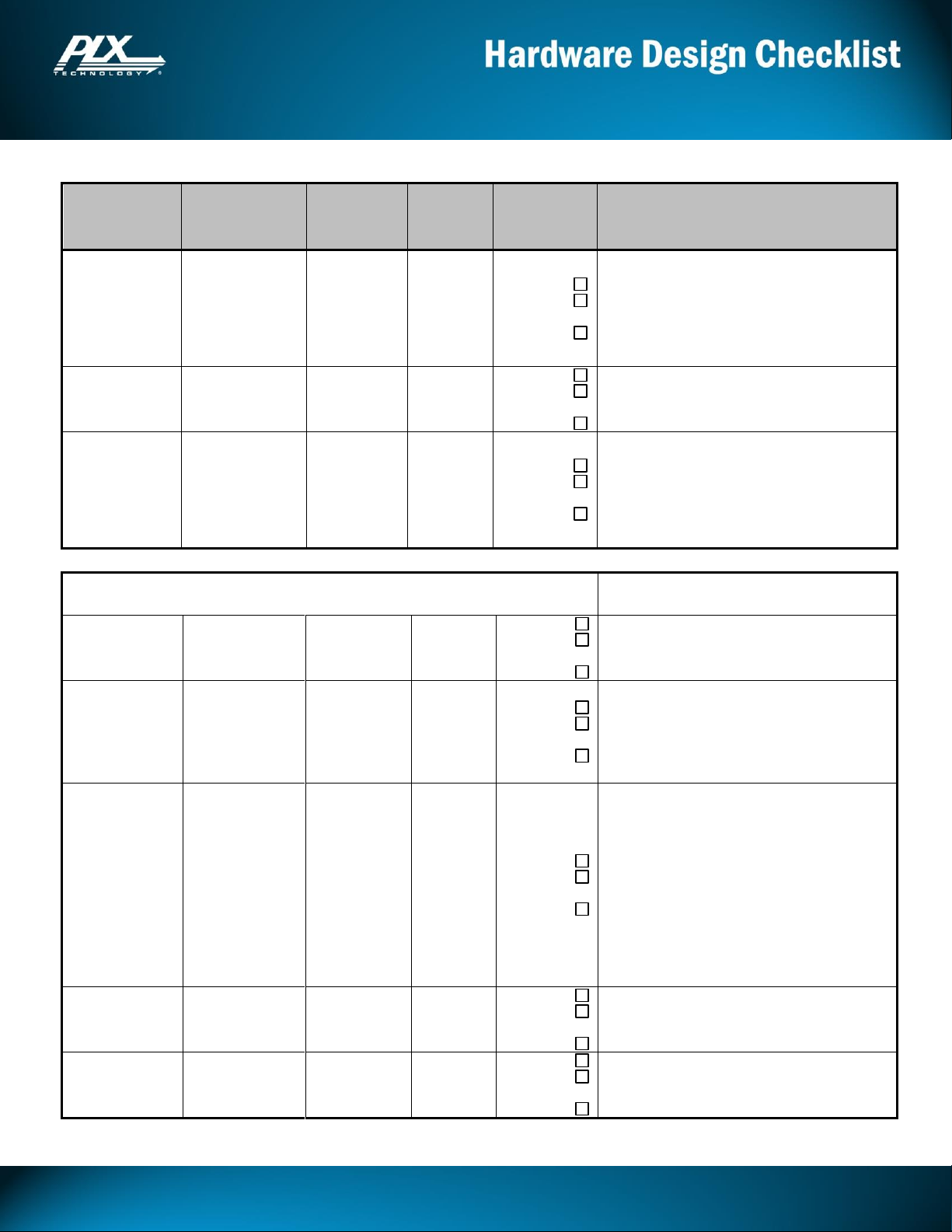
2.4 Clocks
REFCLK Source
Signal Type
Checked
Requirements
External REFCLK Clock
Transmitter
External-CML
YES
NO
UNKNOWN
Frequency Tolerance: ± 300 ppm, max.
33 Ω series (in-line) and 49 Ω shunt (to GND) required on each differential
signal, near the clock source.
Signal Name
Dual-Row
QFN Pkg.
Pin #
TQFP
Package
Pin #
Signal
Type
Checked
Recommendations
PEX_REFCLKn ,
PEX_REFCLKp
B24
A27
52
51
CML Input
YES
NO
UNKNOWN
100 MHz PCI Express Reference Clock input
pair.
Signal Name
Dual-Row
QFN Pkg.
Pin #
TQFP
Package
Pin #
Signal
Type
Checked
Recommendations
PEX_PERST#
B15
32
I
YES
NO
UNKNOWN
PCI Express Reset
Used to initiate a fundamental reset. This reset is
propagated to all downstream ports. Adapter card
designs connect this pin directly to the PCI
Express slot PERST# pin. PEX_PERST# should
remain asserted for 100 ms after power supplies
and clocks are stable.
Signal Name
Dual-Row
QFN Pkg.
Pin #
TQFP
Package
Pin #
Signal
Type
Checked
Recommendations
STRAP_DEBUG_SEL#
C4
30
I
PU
YES
NO
UNKNOWN
Factory Test Only
This signal can be left unconnected in normal
applications. If this ball is connected to a board
circuit trace, it must be externally pulled up to
VDD_IO.
STRAP_FAST_BRINGUP#
A40
78
I
PU
YES
NO
UNKNOWN
Factory Test Only
This signal can be left unconnected in normal
applications. If this ball is connected to a board
circuit trace, it must be externally pulled up to
VDD_IO.
2.4.1 Clock Source and Line Termination
2.4.2 Clock Input Pins
PEX8605
2.5 Reset
2.6 Configuration Straps
These pins should be pulled High (to VDD_IO) or Low (to Ground), through 4.7K-10K ohms, as indicated.
© PLX Technology, www.plxtech.com Page 4 of 13 2 May 2013, version 1.7
Page 5

PEX8605
Signal Name
Dual-Row
QFN Pkg.
Pin #
TQFP
Package
Pin #
Signal
Type
Checked
Recommendations
STRAP_LEGACY
C13
97
I
PU
YES
NO
UNKNOWN
Factory Test Only
Do not connect this pin to board circuit traces.
STRAP_PLL_BYPASS#
C12
96
I
PU
YES
NO
UNKNOWN
Factory Test Only
This signal can be left unconnected in normal
applications. If this ball is connected to a board
circuit trace, it must be externally pulled up to
VDD_IO.
STRAP_PORTCFG
B37
83
I
PD
YES
NO
UNKNOWN
Port Configuration Select
L = x1, x1, x1, x1 (Lane 0 is Port 0 up)
H = x2, x1, x1 (Lanes 1:0 form Port 0 up)
STRAP_PROBE_MODE#
C3
27
I
PU
YES
NO
UNKNOWN
Factory Test Only
This signal can be left unconnected in normal
applications. If this ball is connected to a board
circuit trace, it must be externally pulled up to
VDD_IO.
STRAP_RC_MODE
B35
79
I
PD
YES
NO
UNKNOWN
Factory Test Only
Do not connect this pin to board circuit traces.
STRAP_SERDES_MODE_EN#
A39
76
I
PU
YES
NO
UNKNOWN
Factory Test Only
Do not connect this pin to board circuit traces.
STRAP_SMBUS_EN#
B28
62
I
PU
YES
NO
UNKNOWN
System Management Bus Enable
When pulled or tied to Ground, enables SMBus
Slave protocol on the I2C_SCL0 and I2C_SDA0
2-wire bus
When pulled to VDD_IO or unconnected,
enables I2C Slave protocol on the I2C_SCL0 and
I2C_SDA0 2-wire bus.
STRAP_SSC_CENTER#
C11
93
I
PU
YES
NO
UNKNOWN
Factory Test Only
Do not connect this pin to board circuit traces.
STRAP_TESTMODE[3:0]
C10, C9, C8,
C7
67, 64, 63,
60
[3,1]: I,
PU
[2,0]: I,
PD
YES
NO
UNKNOWN
Factory Test Only (4 Balls)
Ok to leave these pins unconnected. If external
circuit traces are attached to these pins, they must
be strapped as HLHL.
(STRAP_TESTMODE[3,1] pulled to VDD_IO,
STRAP_TESTMODE[2,0] pulled or tied to
Ground)
© PLX Technology, www.plxtech.com Page 5 of 13 2 May 2013, version 1.7
Page 6

PEX8605
Signal Name
Dual-Row
QFN Pkg.
Pin #
TQFP
Package
Pin #
Signal
Type
Checked
Recommendations
STRAP_UPCFG_TIMER_EN#
A28
53
I
PU
YES
NO
UNKNOWN
Link Upconfigure Timer Enable
This input maps to the Debug Control register
UPCFG Timer Enable bit. This signal and its
corresponding register bit must NOT be toggled
at runtime.
When STRAP_UPCFG_TIMER_EN# is pulled
high, the Data Rate Identifier symbol in the TS
Ordered-Sets always advertises support for both
the 5 GT/s (Gen 2) data rate and Autonomous
Change.
When STRAP_UPCFG_TIMER_EN# is pulled
low, if this Link training sequence fails during
the Configuration state, the next time the LTSSM
exits the Detect state, TS Ordered-Sets advertise
only the 2.5 GT/s (Gen1) data rate and no
Autonomous Change. The LTSSM then
continues to toggle between Gen1 and Gen2
advertisement every time it exits Detect state.
NOTE: This feature should only be enabled if a
non-compliant device will not link up when
these Data Rate Indentifier bits are set.
(if adding an option resistor to pull this ball low,
a default pull-up resistor should also be used)
Signal Name
DualRow QFN
Pkg.
Pin #
TQFP
Package
Pin #
Signal
Type
Checked
Recommendations
PEX_PERn[3:0]
A61, B47,
B10, A6
121, 108,
19, 7
CMLRn
YES
NO
UNKNOWN
Negative Half of PCI Express Receiver
Differential Signal Pairs for lanes 2:0 (3 Pins)
PEX_PERp[3:0]
A62, A55,
A11, A5
122, 109,
18, 6
CMLRp
YES
NO
UNKNOWN
Positive Half of PCI Express Receiver
Differential Signal Pairs for lanes 2:0 (3 Pins)
PEX_PETn[3:0]
A59, A52,
A14, A8
117, 104,
23, 11
CMLTn
YES
NO
UNKNOWN
Negative Half of PCI Express Transmitter
Differential Signal for lanes 2:0 (3 Pins)
100 nF AC coupling caps required on all PCI
Express transmit pairs.
PEX_PETp[3:0]
A60, A53,
B11, B6
118, 105,
22, 10
CMLTp
YES
NO
UNKNOWN
Positive Half of PCI Express Transmitter
Differential Signal Pairs for lanes 2:0 (3 Pins)
100 nF AC coupling caps required on all PCI
Express transmit pairs.
2.7 PCI Express Interface
© PLX Technology, www.plxtech.com Page 6 of 13 2 May 2013, version 1.7
Page 7

PEX8605
Signal Name
DualRow
QFN
Pkg.
Pin #
TQFP
Package
Pin #
Signal
Type
Checked
Recommendations
EE_CS#
B32
73
O
YES
NO
UNKNOWN
Serial EEPROM Chip Select Output.
Connect to EEPROM CS# input. Can be left floating if
not used.
EE_DI
A36
71
O
YES
NO
UNKNOWN
Serial EEPROM Data Input (Write Data)
Connect to EEPROM serial data input, SI. Can be left
floating if not used.
Note: This signal requires an external pull-up when
connecting to serial EEPROM. Recommend 4.7K – 10K
Ohms. Rise time of this signal is dependent on the
strength of the external pull-up.
EE_DO
B33
75
I/PU
YES
NO
UNKNOWN
Serial EEPROM Data Output (Read Data)
Connect to EEPROM serial data output, SO. Weakly
pulled up. Should be externally pulled high to VDD25
EE_SK
A38
74
O
YES
NO
UNKNOWN
Serial EEPROM Clock Output
Connect to EEPROM clock input, SCK. Can be left
floating if not used.
2.8 Serial EEPROM
As of this writing, a serial configuration EEPROM is not required for the PEX8605. Use of a serial
configuration EEPROM in systems designs is optional. However, we highly recommend including the serial
EEPROM circuit as a stuffing option, to allow inclusion of EEPROM-based performance enhancements
and/or errata workarounds that may become available in the future.
2.8.1 Serial EEPROM Type
If implementing serial EEPROM, use Microchip Technology, Inc. p/n 25AA128 or equivalent for
programming the PEX8605. Be sure to specify the ‘-1.8’ version of the part, which can support operation at
VCC voltage of 2.5Volts. Power the device from the VDD_IO supply, bypassed with 0.1 uF.
2.8.2 Serial EEPROM Interface – 4 Pins
2.8.3 Additional EEPROM Signals
WP#: Tie to EEPROM VCC if not used, else jumper to GND to enable write-protect.
HOLD#: Tie to EEPROM VCC
© PLX Technology, www.plxtech.com Page 7 of 13 2 May 2013, version 1.7
Page 8

2.9 JTAG Interface – 5 Pins
Signal
Name
DualRow
QFN
Pkg.
Pin #
TQFP
Package
Pin #
Signal
Type
Checked
Recommendations
JTAG_TCK
A48
94
I
PU
YES
NO
UNKNOWN
JTAG Test Clock Input
Frequency can be from 0 to 10 MHz.
This signal is internally pulled up to VDD2.5 through a weak
pull-up resistor. If this pin is connected to external board
circuits, an external pull-up is also recommended.
JTAG_TDI
A47
91
I
PU
YES
NO
UNKNOWN
JTAG Test Data Input
This signal is internally pulled up to VDD2.5 through a weak
pull-up resistor. If this pin is connected to external board
circuits, an external pull-up is also recommended.
JTAG_TDO
B29
65
O
YES
NO
UNKNOWN
JTAG Test Data Output
Serial output from the JTAG TAP Controller test instructions
and data. Can be left open (no connect) if JTAG interface is
not used.
JTAG_TMS
B42
95
I
PU
YES
NO
UNKNOWN
JTAG Test Mode Select
This signal is internally pulled up to VDD2.5 through a weak
pull-up resistor. If this pin is connected to external board
circuits, an external pull-up is also recommended.
JTAG_TRST#
A34
66
I
PU
YES
NO
UNKNOWN
JTAG Test Reset
Pull to GROUND (VSS) through 1.5K ohms for normal
operation
Signal Name
Dual-Row
QFN Pkg.
Pin #
TQFP
Package
Pin #
Signal
Type
Checked
Recommendations
I2C_ADDR[2:0]
A41, B36,
A42
80, 81, 82
I
PU
YES
NO
UNKNOWN
I²C Slave Address Bits 2 through 0 (3 Pins)
Used to configure the device address on the I²C Bus. If I²C or
PEX_INTA# output is used, I2C_ADDR[2:0] should be
strapped to a unique address, to avoid address conflict with
any other I²C devices (on the same I²C Bus segment) that have
the upper four bits of their 7-bit I²C Slave address also Set to
1011b. Must be pulled High to VDD25 or Low to VSS (GND)
through external resistors.
I2C_SCL
A45
87
OD
YES
NO
UNKNOWN
I²C Serial Clock
I²C Clock source. This signal must be pulled high to VDD_IO.
Refer to the I2C specification for details.
I2C_SDA0
B39
88
OD
YES
NO
UNKNOWN
I²C Serial Data
Transfers and receives I²C data. This signal must be pulled
high to VDD_IO. Refer to the I2C specification for details.
PEX8605
2.10 I²C Slave Interface Signals – 5 Pins
© PLX Technology, www.plxtech.com Page 8 of 13 2 May 2013, version 1.7
Page 9

Signal Name
Dual-Row
QFN Pkg.
Pin #
TQFP
Package
Pin #
Signal
Type
Checked
Recommendations
FATAL_ERR#
B40
90
O
YES
NO
UNKNOWN
Fatal Error Output
Used to signal fatal error condition to other devices,
or to light status LED, etc. If FATAL_ERR# is not
used, ok to leave this pin unconnected.
HP_PRSNT#
B25
55
I/O
PU
YES
NO
UNKNOWN
Hot Plug PRSNT# Input
Active-low slot control logic input that connects to
the PCI Express slot’s PRSNT# signal, which is
typically grounded. See the data book for details.
If used, this pin should be externally pulled high to
VDD_IO. Otherwise, ok to leave unconnected.
LANE_GOOD[3:0]#
B16, B55,
A16, A19
35, 125, 28,
36
I/O
YES
NO
UNKNOWN
Active-Low PCI Express Lane Linkup Status
Indicator Outputs for lanes 3:0 (4 Pins)
These signals can directly drive common-anode
LED modules (external current-limiting resistors
are required). Alternate function for each pin is
GPIOn. See the data book for details on use.
MFG_AMC
C5
31
I
PD
YES
NO
UNKNOWN
Factory Test Only
Do not connect this pin to board electrical paths.
MFG_TAPEN
C6
34
I
PD
YES
NO
UNKNOWN
Factory Test Only
Do not connect this pin to board electrical paths.
MFG_TMC1
C15
126
I
PD
YES
NO
UNKNOWN
Factory Test Only
Do not connect this pin to board electrical paths.
MFG_TMC2
C16
1
I
PD
YES
NO
UNKNOWN
Factory Test Only
Do not connect this pin to board electrical paths.
PEX_INTA#
B34
77
OD
YES
NO
UNKNOWN
Interrupt Output
If used, PEX_INTA# should be pulled high to
VDD_IO through 4.7K Ohms. If not used, ok to
leave this pin unconnected.
PROCMON
C14
100
O
YES
NO
UNKNOWN
Factory Test Only
Do not connect this pin to board electrical paths.
2.11 Device-Specific Signals
PEX8605
© PLX Technology, www.plxtech.com Page 9 of 13 2 May 2013, version 1.7
Page 10

PEX8605
Signal Name
Dual-Row
QFN Pkg.
Pin #
TQFP
Package
Pin #
Signal
Type
Checked
Recommendations
PWRON_RST#
B14
29
I/O
PU
YES
NO
UNKNOWN
Power-On Reset
When stand-by (Vaux) power is implemented, and
where remote wake up using WAKE# or
beacon signaling from D3cold power state has to be
forwarded, PWRON_RST# must be held high when
device is in D3cold power state.
If stand-by power is not implemented, connect this
signal to PEX_PERST#.
WAKE#
B56
128
OD
YES
NO
UNKNOWN
PCI Express WAKE#
If VAUX_IO power rail is implemented, WAKE#
signal should be externally pulled high to
VAUX_IO. Otherwise, pull high to VDD_IO.
XTAL_IN
B30
68
I/O
PU
YES
NO
UNKNOWN
Factory Test Only
Pull or tie directly to Ground.
Signal Name
DualRow
QFN
Pkg.
Pin #
TQFP
Package
Pin #
Signal
Type
Checked
Recommendations
PEX_REFCLK_OUTp1
A24
45
HCSLOUT
YES
NO
UNKNOWN
Positive Half of Reference Clock Output Pair 1
Note: No termination resistor networks are required
for REFCLK output pairs.
PEX_REFCLK_OUTn1
B21
46
HCSLOUT
YES
NO
UNKNOWN
Negative Half of Reference Clock Output Pair 1
PEX_REFCLK_OUTp2
A22
41
HCSLOUT
YES
NO
UNKNOWN
Positive Half of Reference Clock Output Pair 2
PEX_REFCLK_OUTn2
A23
43
HCSLOUT
YES
NO
UNKNOWN
Negative Half of Reference Clock Output Pair 2
PEX_REFCLK_OUTp3
A20
38
HCSLOUT
YES
NO
UNKNOWN
Positive Half of Reference Clock Output Pair 3
PEX_REFCLK_OUTn3
A21
39
HCSLOUT
YES
NO
UNKNOWN
Negative Half of Reference Clock Output Pair 3
2.12 PCI Express Reference Clock Outputs
© PLX Technology, www.plxtech.com Page 10 of 13 2 May 2013, version 1.7
Page 11

Signal Name
DualRow
QFN
Pkg.
Pin #
TQFP
Package
Pin #
Signal
Type
Checked
Recommendations
PEX_REFCLK_OUT_BIAS
B22
48
A
YES
NO
UNKNOWN
Optional Bias Voltage Input
This pin can be left un-connected for typical
applications. Suggest routing this pin to a test
point.
PEX_REFCLK_OUT_RREF
B23
50
A
YES
NO
UNKNOWN
External Reference Resistor
Connect this pin to Ground through a 2.00K Ohms,
1% resistor. Place resistor close to the pin.
Signal
Name
Dual-Row QFN
Pkg.
Pin #
TQFP
Package
Pin #
Signal
Type
Checked
Recommendations
N/C
A1, A2, A3, A4, A17,
A33, A35, A44, A49,
B1, B2, B38, C1, C2
2, 69, 85, 86
N/C
YES
NO
UNKNOWN
No-Connect (QFN: 14 pins, TQFP: 4 pins)
No function. Do not connect these pins to board
electrical paths.
2.13 No-Connect Signals
Do not connect these pins to board electrical paths.
PEX8605
© PLX Technology, www.plxtech.com Page 11 of 13 2 May 2013, version 1.7
Page 12

PEX8605
2.14 Additional Schematic Design Considerations
2.14.1 Mid-Bus Probe Points
If your design contains embedded PCI Express links, it can sometimes be useful to add probe pads to your
PCB design to allow instrumentation access to PCI Express links on the board. If you are planning to include
mid-bus probe footprints in your PCB design, be aware that they may induce jitter and/or reduce signal
integrity on the PCI Express lanes it is connected to. Refer to your instrumentation vendor’s specifications for
specific layout design considerations.
2.14.2 Spread Spectrum Clocking (SSC)
The PEX8605 supports a Spread Spectrum REFCLK source. The SSC clock must originate from the PCI
Express connector on a slot in the motherboard or through a common clock source that is being distributed to
all add-in cards and/or PCI Express devices in the system.
If your REFCLK source is non-SSC, then you may have separate REFCLK sources on different cards or
devices as long as their frequency difference is within ± 300ppm. (~30ps for a 100MHz Clock source) Refer
to the PEX8605 data book for more information.
3 PCB Layout Design Checks
Note: The following guidelines were provided for PCI Express 2.5 GT/s (Gen 1) transmission lines. On the
Gen 2 PCI Express 5.0 GT/s signaling by increasing the pre-emphasis and increasing receiver sensitivity are
supposed to counteract the bandwidth related losses associated with the frequency increase. However, as
frequency goes up, other discontinuities become more of a factor not just the simple channel loss. We strongly
recommend you simulate and verify your design at the operating frequency. HSPICE models are available on
the PLX website.
Since PCI Express links operate at very high speeds, proper PCB routing of each RX and TX pair in each lane
is critical for maintaining signal integrity on each PCI Express link. The PCI-SIG provides numerous
suggestions about how to correctly design PCB’s containing PCI Express links. Several important guidelines
for proper layout of PCI Express SerDes signals are listed below. Additional information is available from the
PCI-SIG website, www.pci-sig.com.
1. Recommended Microstrip Trace Impedance:
Differential Impedance: 85 Ω ± 20%
Single ended Impedance: 55 Ω ± 15%
2. Recommended Stripline Trace Impedance:
Differential Impedance: 85 Ω ± 15%
Single ended Impedance: 55 Ω ± 15%
3. Maintain ≥ 20 mil trace edge to plane edge gap
4. Match signal trace lengths to within 5 mils. Equalize using a snaked trace near the receive end if needed, but avoid
"tight bends"
5. Route signals over continuous, un-broken planes.
6. Use GND-GND stitching vias near signal vias when routing between PCB layers
7. Do not route over plane splits or voids. Allow no more than 1/2 trace width routed over via antipad
© PLX Technology, www.plxtech.com Page 12 of 13 2 May 2013, version 1.7
Page 13

PEX8605
8. Match left/right turn bends where possible. No 90-degree bends or "tight" bend structures.
9. The reference clock signal pair should maintain the same reference plane for the entire routed length and should not
cross any plane splits (breaks in the reference plane)
10. Reference clock terminating components should be placed as close as possible to their respective driving sources,
ideally within 100 mils of the clock/receiver component pin/pin.
11. Match all segment lengths between differential pairs along the entire length of the pair.
12. Maintain constant line impedance along the routing path by keeping the same line width and line separation.
13. Avoid routing differential pairs adjacent to noisy signal lines or high speed switching devices such as clock chips.
14. Recommended reference clock differential pair spacing (clock to clock#) ≤ 11.25 mils.
15. Recommended reference clock trace spacing to other traces is ≥ 20 mils.
16. Recommended reference clock line width ≥ 5 mils.
17. When routing the 100MHz differential clock, do not divide the two halves of the clock pair between layers.
18. Recommended reference clock differential impedance: 85 Ω ± 15%
19. Recommended PCI Express reference clock to PCI express reference clock length matching to within 25 mils
20. AC Coupling Capacitors: The same package size and value of capacitor should be used for each signal in a
differential pair. Refer to the PCI Express Base Specification for permitted values.
21. AC Coupling Capacitors: Locate capacitors for coupled traces in a differential pair at the same location along the
differential traces. Place them as close to each other as possible.
22. AC Coupling Capacitors: The "breakout" into and out of the capacitor mounting pads should be symmetrical for
both signal lines in a differential pair. In addition, the area under the cap footprint should be voided of metal.
23. Test points and probing structures should not introduce stubs on the differential pairs.
24. Use Low ESR, ceramic caps for lane AC-coupling.
4 Assembly Guidelines for aQFN Packages
PEX8605 assembly guidelines are provided in an application note entitled “aQFN Surface Mount Application
Note”. This document is available for download in the PEX8605 web toolbox, www.plxtech.com/pex8605.
This document covers important points for proper assembly of aQFN packages, including center pad layout,
stencil design, and assembly process steps. Designers should review these procedures with their assembly
house to insure reliable PCB assembly.
© PLX Technology, www.plxtech.com Page 13 of 13 2 May 2013, version 1.7
 Loading...