

Page 1
MGA-725M4 Demonstration PCB
Assembly and Operating Instructions
Demonstration Guide
Introduction
Applies to DEMO_MGA_725M4 PCB and MGA-725M4
RFIC.
Description
The MGA-725M4 is a single-stage, low noise amplifier
with an integrated bypass switch. For detailed specifications and operation, refer to the MGA-725M4 Data
Sheet. The DEMO_MGA_725M4 printed circuit board,
illustrated in Figure 1, is designed to demonstrate the
performance of the MGA-725M4 RFIC amplifier/bypass switch for your specific application.
This circuit board is of a general purpose design and
may be used for applications covering a wide range of
frequencies. The particular component values listed
below have been optimized for use in 1.9 GHz systems.
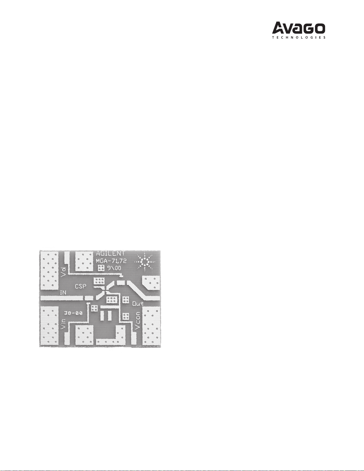
The demonstration circuit is fabricated on a 0.031-inch
thick GETEK®1 G200D (εr = 4.2) dielectric material.
The amplifier and related components are assembled
onto the printed circuit board as shown in Figure 2.
This layout is designed to use edge-mounting SMA
connectors, such as the EF Johnson 142-0701-881, for
the RF connections. This type of connector slips over
the edge of the board without the need for drilling
holes. The center conductors are soldered to the input
and output microstrip lines and the ground pins of the
connectors are soldered to the ground plane on the
backside of the board and to the ground pads on the
topside. The DC terminals and adjacent ground pads
are designed to fit a 2-pin, 0.100" centerline flat header
of the type commonly used on computer boards (e.g.
Waldom-Molex 4030 series) as a connection to the
power supply and/or control voltages.
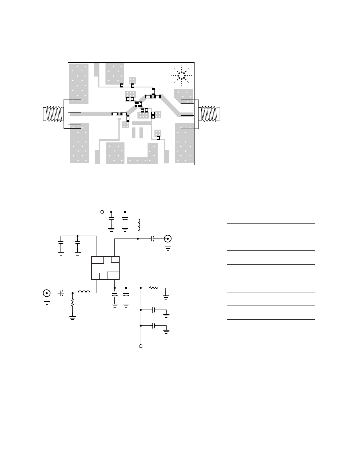
A schematic diagram of the circuit is shown in Figure
3 with component values in Table 1. The values listed
have been selected for use at 1900 MHz. Inductor L1 is
used with the MGA-725M4 to improve the input power
match.
Figure 1. Unassembled Demonstration Board.
DC blocking capacitors (C1 and C2) have been included at the input and output to isolate device voltages
from adjacent circuits or test equipment. DC power is
supplied to the amplifier through the RF output pin by
means of a bias decoupling network which consists of
a RF choke (RFC) and bypass capacitors.
Page 2
AGILENT
MGA-71, 72
9/00
L1
R1
AH
C5
C
C4
C6
SC
R2
C
RFC
C2
Out
Vd
IN
CSP
C0
C3
C1
C0
Vin
Vcon
Figure 2. Assembled Demonstration Circuit with Component Reference Designators.
V
d
C3 C4
RF INPUT
C1
R1
C0
1
AH
3
L1
C5
C
RFC
C2
RF OUTPUT
2
4
C6
R2
(R BIAS)
C
Table 1. List of Component Values.
R1 = 1 kΩ
R2 = See text
L1 = 3.9 nH
RFC = 22 nH
SC = SC
C (2 ea) = 100 pF
C0
V
CON
Figure 3. Schematic Diagram of MGA-725M4 Demonstration Board.
2
C0 (2 ea) = 1000 pF
C1, C2 = 47 pF
C3, C6 = 30 pF
C4, C5 = 22 pF
Page 3

Setting Device Current
The MGA-725M4 incorporates an
adjustable bias feature. The
MGA-725M4 is typically operated
within a device current range of
10-60 mA. A current of 10-20 mA
is appropriate for LNA
applications. Biasing the amplifier
at currents of 40-60 mA allows it
to deliver higher output power
levels for use as a transmit driver
stage.
Device current is set by the
resistance between Pin 4 (or
Pin 1) of the MGA-725M4 and DC
ground. For evaluation purposes,
an external resistor is suggested
for setting the bias current. The
external resistor is connected
between the Vcon terminal and
ground. Alternatively, the current
can be fixed by installing resistor
R2 onto the PCB as indicated in
Figure 2 and in the schematic
diagram in Figure 3. The
approximate value of the
current-setting resistor is
calculated from:
=
964
I
d
1 - 0.112
I
d
R
bias
Operation
To operate the MGA-725M4
demonstration amplifier, it is only
necessary to apply +3 volts to the
+V
connection. If an on-board
d
resistor is used to set the current,
the V
terminal is left open.
con
Switch Bypass Mode
The MGA-725M4 is placed in the
bypass mode by setting the device
current to zero. This is done by
open-circuiting the bias resistor,
R
.
bias
A Note on Performance
Actual performance of the
MGA-725M4 as measured in the
demonstration circuit may not
exactly match the data sheet
specifications. The circuit board
material, passive components, RF
bypasses and connectors all
introduce losses and parasitics
that degrade device performance.
For this demonstration circuit,
circuit losses of about 0.3 dB
would be expected at both the
input and output sides of the
RFIC at 2 GHz.
Where R
is in ohms and Id is
bias
the desired device current in mA.
If desired, the MGA-725M4 can
also be biased by directly
grounding device Pins 1 and 4 and
applying a negative control
voltage to Pin 3. The connection
labeled Vin is provided for this
purpose. (Note : R
bias
is not
used with this method of biasing.)
3
Page 4

For product information and a complete list of distributors, please go to our web site:
Avago, Avago Technologies, and the A logo are trademarks of Avago Technologies, Limited in the United States and other countries.
Data subject to change. Copyright © 2007 Avago Technologies, Limited. All rights reserved.
5988-0586EN - May 31, 2007
www.avagotech.com
 Loading...