

Page 1
Revision 07/13/01 @ 4:56 PM Page 1
W-CDMA application using MGA-71543, a Low
Noise Amplifier with Bypass Switch.
_________________________
INTRODUCTION:
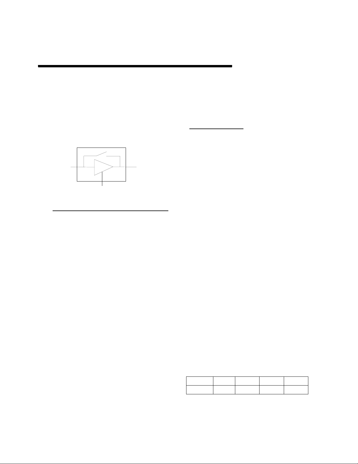
The MGA-71543 is a single stage GaAs RFIC
low noise amplifier with an integrated bypass
switch (Figure 1).
RF IN
SW & Bias Control
Figure 1. MGA-71543. Functional Diagram
The purpose of the switch feature is to prevent
distortion of high signal levels in receiver
applications by bypassing the amplifier.
Furthermore it saves current thus improving
battery life.
One of the two ground leads of the amplifier is
tied to the control leads of the switch to allow
simple control of the bias. Therefore, using one
of the ground leads, it is possible to vary the bias
current (including completely shutting down t he
amplifier) by varying the resistor to ground that
is attached to it.
In short, the MGA-71543 is a small LNA/Bypass
Switch MMIC that provides a low Noise figure,
a high gain and high third order input intercept
point (IIP3) especially suitable for the LNA stage
for W-CDMA application.
This application note describes a W-CDMA Low
noise amplifier design using Agilent
Technologies’ MGA-71543.
RF OUT
for ease, if tuning is necessary and also as a
safety to avoid any possible oscillations).
Matching and biasing
A simple ser ies-shunt network of 1.5nH and
4.7nH at the input provides the noise matching
and the necessary DC grounding (of the input
pin). Because the main active device is a
depletion mode FET, source-biasing technique is
used so that only one positive DC supply is
required at the output. The input (gate) is DC
grounded and the source is RF bypassed, while
current setting resistors (R20 or R21) are
attached to ground.
A simple shunt-series network of 3.9nH and
1.8pF at the output does the required matching
for linearity while providing the RF choking and
DC blocking. The output-matching network does
not affect the noise figure, which was already set
by the input matching.
R38 and R25 provide some resistor loading at
low frequency and help stabilize the device at
low frequency. The rest of the components used,
including bypass capacitors (C8, C36, C37, C44,
C47), current setting resistors (R20 or R21),
voltage drop resistor (R24), DC block capacitors,
are all listed in table 1.
Performance Results
It is possible to achieve 3.7dBm of input Third
order intercept Point (IIP3) at 2.1GHz with a
device current of 11mA.
Conclusion
The MGA-71543 can be used for W-CDMA
application with the following typical
performance summary data:
Design overview and summary:
The board used for this design is shown i n
figure2. The schematic of this board is shown
in figure 3. The number of components used
can be reduced in a real application circuit
because some jumpers (0 Ω resistors), and
bypass capacitors could be eliminated without
performance degradation (some are only used
NF Gain IIP3 S11 S22
1.2 15 3.7 13 8
Current = 11mA
Frequency: 2 .1GHz
Page 2
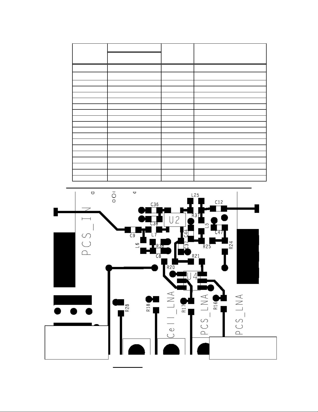
Designation B
Description4 layer Board
WCDMA-2100
Part Number Package
U2 or 71
U4 or 03 Switch b/n Gnd resistors FDG6303N Dual N-channel, Digital FET
C12 1.8 pF
C8
C9 5.6 pF
C38 Not used
C36, C37, C44 82, 82, 27 pF
C47
L5 3.9 nH
L6 4.7 nH
L7 1.5 nH
L25 Not used For tuning / Not used here
R38
R20
R21
R24, R25
R16,R17
R37
R18,R28 Not Used Used for other current setting
*
DUT
0.033 µµµµF
0.033 µµµµF
51 ΩΩΩΩ
36 Ω
56 ΩΩΩΩ
6.2 ΩΩΩΩ
0 ΩΩΩΩ
0 ΩΩΩΩ
MGA-71543 SOT-343 (SC-70) / Switch LNA
Size 0402/Output match, DC block
Size 0402 / Bypass capacitor
Size 0402 / DC block capacitor
Size 0402 / Bypass capacitors
Size 0402 / Bypass capacitor
TOK LL1005 0402/Out match/RF choke,DC feed
TOK LL1005 Size 0402 / input noise matching
TOK LL1005 Size 0402 / input noise matching
Size 0402
Size 0402 / set Id for 16mA Bias
Size 0402 / set Id for 10.5mA Bias
R24Drop voltage,R25resistive load
Size 0402 (Jumper)
0402 Jumper or replace with a stub
Table 1. Component Values for 2100 MHz amplifier on smaller board
Software
controlling the
switch
Manual switch
control
Figure 2. Test board layout
2
Page 3

C9
L7
MGA-71543
U4 = FDG6303N
Dual N-channel, Digit al
FET
R38
C12
OUTIN
Figure 3. Test board layout a nd
schematic
L6
R17 (0 Ω Jumper)
L5
C47
R25
R24
R16 (0 Ω Jumper)
C8
R38
R20
FDG63 03N
R21
C37
C44
Selects current
set by R21
Selects current
3
set by R20
Vd=3 Volt
 Loading...