

Page 1

TECHNICAL
MANUAL
LSI53C875/875E
PCI to Ultra SCSI
I/O Processor
Version 4.2
April 2003
®
DB14-000165-01
Page 2

This document contains proprietary information of LSI Logic Corporation. The
information contained herein is not to be used by or disclosed to third parties
without the express written permission of an officer of LSI Logic Corporation.
LSI Logic products are not intended for use in life-support appliances, devices,
or systems. Use of any LSI Logic product in such applications without written
consent of the appropriate LSI Logic officer is prohibited.
Document DB14-000165-01, Sixth Edition (April 2003)
This document describes the LSI Logic LSI53C875/875E PCI to Ultra SCSI I/O
Processor and will remain the official reference source for all revisions/releases
of this product until rescinded by an update.
To receive product literature, visit us at http://www.lsilogic.com.
LSI Logic Corporation reserves the right to make changes to any products herein
at any time without notice. LSI Logic does not assume any responsibility or
liability arising out of the application or use of any product described herein,
except as expressly agreed to in writing by LSI Logic; nor does the purchase or
use of a product from LSI Logic convey a license under any patent rights,
copyrights, trademark rights, or any other of the intellectual property rights of
LSI Logic or third parties.
Copyright © 1998–2001/2003 by LSI Logic Corporation. All rights reserved.
TRADEMARK ACKNOWLEDGMENT
The LSI Logic logo design, TolerANT, SDMS, and SCRIPTS are registered
trademarks or trademarks of LSI Logic Corporation. All other brand and product
names may be trademarks of their respective companies.
ii
Page 3

Audience
Organization
Preface
This book is the primary reference and technical manual for the LSI Logic
LSI53C875/875E PCI to Ultra SCSI I/O Processor.It contains a complete
functional description for the LSI53C875/875E and includes complete
physical and electrical specifications for the LSI53C875/875E.
This technical manual is intended for system designers and programmers
who are using this device to design a SCSI port for PCI-based personal
computers, workstations, or embedded applications.
This document has the following chapters and appendixes:
• Chapter 1, General Description, includes general information about
the LSI53C875 and other members of the LSI53C8XX family of PCI
to SCSI I/O Processors.
• Chapter 2, Functional Description, describes the main functional
areas of the chip in more detail, including the interfaces to the SCSI
bus.
• Chapter 3, PCI Functional Description, describes the chip’s
connection to the PCI bus, including the PCI commands and
configuration registers supported.
• Chapter 4, Signal Descriptions, contains the pin diagrams and
definitions of each signal.
• Chapter 5, SCSI Operating Registers, describes each bit in the
operating registers, organized by address.
Preface iii
Page 4

• Chapter 6, Instruction Set of the I/O Processor, defines all of the
• Chapter 7, Instruction Set of the I/O Processor, contains the
• Appendix A, Register Summary, is a register summary.
• Appendix B, External Memory Interface Diagram Examples,
Related Publications
For background information, please contact:
ANSI
11 West 42nd Street
New York, NY 10036
(212) 642-4900
Ask for document number X3.131-199X (SCSI-2)
Global Engineering Documents
15 Inverness Way East
Englewood, CO 80112
(800) 854-7179 or (303) 397-7956 (outside U.S.) FAX (303) 397-2740
Ask for document number X3.131-1994 (SCSI-2); X3.253 (SCSI-3
Parallel Interface)
SCSI SCRIPTS instructions that are supported by the LSI53C875.
electrical characteristics and AC timings for the chip.
contains several example interface drawings to connect the
LSI53C875 to an external ROM.
ENDL Publications
14426 Black Walnut Court
Saratoga, CA 95070
(408) 867-6642
Document names: SCSI Bench Reference, SCSI Encyclopedia, SCSI
Tutor
Prentice Hall
113 Sylvan Avenue
Englewood Cliffs, NJ 07632
(800) 947-7700
Ask for document number ISBN 0-13-796855-8, SCSI: Understanding
the Small Computer System Interface
iv Preface
Page 5

LSI Logic World Wide Web Home Page
www.lsilogic.com
SCSI SCRIPTS™ Processors Programming Guide, Version 2.2,
Order Number S14044.A
PCI Special Interest Group
2575 N. E. Katherine
Hillsboro, OR 97214
(800) 433-5177; (503) 693-6232 (International); FAX (503) 693-8344
Conventions Used in This Manual
The word assert means to drive a signal true or active. The word
deassert means to drive a signal false or inactive.
Hexadecimal numbers are indicated by the prefix “0x” —for example,
0x32CF. Binary numbers are indicated by the prefix “0b” —for example,
0b0011.0010.1100.1111.
Revision Record
Revision Date Remarks
1.0 6/95 Revision 1.0
2.0 3/96 Revision 2.0. Fast-20 changed to Ultra SCSI throughout.
3.0 9/96 Revision 3.0. Minor copy changes throughout.
4.0 2/98 Revision 4.0. Minor copy changes throughout
4.1 3/01 Product names changed from SYM to LSI.
4.2 4/03 Revision 4.2. Correct V
Preface v
-S in Table 4.3
DD
Page 6

vi Preface
Page 7

Contents
Chapter 1 General Description
1.1 Package and Feature Options 1-4
1.2 Benefits of Ultra SCSI 1-4
1.3 TolerANT®Technology 1-5
1.4 LSI53C875 Benefits Summary 1-6
1.4.1 SCSI Performance 1-6
1.4.2 PCI Performance 1-7
1.4.3 Integration 1-7
1.4.4 Ease of Use 1-7
1.4.5 Flexibility 1-8
1.4.6 Reliability 1-9
1.4.7 Testability 1-9
Chapter 2 Functional Description
2.1 SCSI Functional Description 2-1
2.1.1 SCSI Core 2-1
2.1.2 DMA Core 2-2
2.1.3 SCRIPTS Processor 2-2
2.1.4 Internal SCRIPTS RAM 2-3
2.1.5 SDMS Software: The Total SCSI Solution 2-3
2.2 Designing an Ultra SCSI System 2-4
2.2.1 Using the SCSI Clock Doubler 2-4
2.3 Prefetching SCRIPTS Instructions 2-5
2.3.1 Opcode Fetch Burst Capability 2-6
2.4 External Memory Interface 2-6
2.5 PCI Cache Mode 2-8
2.5.1 Load/Store Instructions 2-8
2.5.2 3.3 V/5 V PCI Interface 2-9
2.5.3 Additional Access to General Purpose Pins 2-9
Contents vii
Page 8

2.5.4 JTAG Boundary Scan Testing 2-10
2.5.5 Big and Little Endian Support 2-10
2.5.6 Loopback Mode 2-12
2.5.7 Parity Options 2-12
2.5.8 DMA FIFO 2-15
2.5.9 SCSI Bus Interface 2-19
2.5.10 Select/Reselect During Selection/Reselection 2-25
2.5.11 Synchronous Operation 2-25
2.5.12 Ultra SCSI Synchronous Data Transfers 2-27
2.5.13 Interrupt Handling 2-28
2.5.14 Chained Block Moves 2-34
2.6 Power Management 2-38
2.6.1 Power State D0 2-38
2.6.2 Power State D3 2-39
Chapter 3 PCI Functional Description
3.1 PCI Addressing 3-1
3.1.1 PCI Bus Commands and Functions Supported 3-2
3.2 PCI Cache Mode 3-4
3.2.1 Support for PCI Cache Line Size Register 3-4
3.2.2 Selection of Cache Line Size 3-5
3.2.3 Alignment 3-5
3.2.4 Memory Move Misalignment 3-6
3.2.5 Memory Write and Invalidate Command 3-6
3.2.6 Memory Read Line Command 3-8
3.2.7 Memory Read Multiple Command 3-9
3.3 Configuration Registers 3-11
Chapter 4 Signal Descriptions
4.1 MAD Bus Programming 4-22
Chapter 5 SCSI Operating Registers
Chapter 6 Instruction Set of the I/O Processor
6.1 SCSI SCRIPTS 6-1
6.1.1 Sample Operation 6-3
viii Contents
Page 9

6.2 Block Move Instructions 6-5
6.2.1 First Dword 6-5
6.2.2 Second Dword 6-12
6.3 I/O Instruction 6-12
6.3.1 First Dword 6-12
6.3.2 Second Dword 6-21
6.4 Read/Write Instructions 6-21
6.4.1 First Dword 6-21
6.4.2 Second Dword 6-22
6.4.3 Read-Modify-Write Cycles 6-22
6.4.4 Move To/From SFBR Cycles 6-24
6.5 Transfer Control Instructions 6-26
6.5.1 First Dword 6-26
6.5.2 Second Dword 6-33
6.6 Memory Move Instructions 6-33
6.6.1 Read/Write System Memory from SCRIPTS 6-34
6.6.2 Second Dword 6-35
6.6.3 Third Dword 6-35
6.7 Load and Store Instructions 6-37
6.7.1 First Dword 6-38
6.7.2 Second Dword 6-39
Chapter 7 Instruction Set of the I/O Processor
7.1 DC Characteristics 7-1
7.2 TolerANT Technology Electrical Characteristics 7-7
7.3 AC Characteristics 7-10
7.4 PCI and External Memory Interface Timing Diagrams 7-13
7.4.1 Target Timing 7-15
7.4.2 Initiator Timing 7-24
7.4.3 External Memory Timing 7-32
7.5 PCI and External Memory Interface Timing 7-50
7.6 SCSI Timing Diagrams 7-51
7.7 Package Drawings 7-58
Appendix A Register Summary
Appendix B External Memory Interface Diagram Examples
Contents ix
Page 10

Figures
Index
Customer Feedback
1.1 LSI53C875 External Memory Interface 1-2
1.2 LSI53C875 Chip Block Diagram 1-3
2.1 DMA FIFO Sections 2-15
2.2 LSI53C875 Host Interface Data Paths 2-16
2.3 Differential Wiring Diagram 2-22
2.4 Regulated Termination 2-24
2.5 Determining the Synchronous Transfer Rate 2-26
2.6 Block Move and Chained Block Move Instructions 2-35
4.1 LSI53C875 Pin Diagram 4-2
4.2 LSI53C875J Pin Diagram 4-3
4.3 LSI53C875N Pin Diagram 4-4
4.4 LSI53C875JB Pin Diagram (Top View) 4-5
4.5 LSI53C875 Functional Signal Grouping 4-9
6.1 SCRIPTS Overview 6-4
6.2 Block Move Instruction Register 6-7
6.3 I/O Instruction Register 6-15
6.4 Read/Write Instruction Register 6-23
6.5 Transfer Control Instructions 6-28
6.6 Memory Move Instruction 6-36
6.7 Load and Store Instruction Format 6-40
7.1 Rise and Fall Time Test Conditions 7-8
7.2 SCSI Input Filtering 7-8
7.3 Hysteresis of SCSI Receiver 7-9
7.4 Input Current as a Function of Input Voltage 7-9
7.5 Output Current as Function of Output Voltage 7-10
7.6 Clock Waveforms 7-11
7.7 Reset Input 7-12
7.8 Interrupt Output 7-13
7.9 PCI Configuration Register Read 7-15
7.10 PCI Configuration Register Write 7-16
7.11 Operating Register/SCRIPTS RAM Read 7-17
x Contents
Page 11

7.12 Operating Register/SCRIPTS RAM Write 7-18
7.13 External Memory Read 7-20
7.14 External Memory Write 7-22
7.15 Opcode Fetch, Nonburst 7-24
7.16 Burst Opcode Fetch 7-25
7.17 Back-to-Back Read 7-26
7.18 Back-to-Back Write 7-27
7.19 Burst Read 7-28
7.20 Burst Write 7-30
7.21 Read Cycle, Normal/Fast Memory ( 64 Kbytes),
Single Byte Access 7-32
7.22 Write Cycle, Normal/Fast Memory ( 64 Kbytes),
Single Byte Access 7-34
7.23 Read Cycle, Normal/Fast Memory ( 64 Kbyte),
Multiple Byte Access 7-36
7.24 Write Cycle, Normal/Fast Memory ( 64 Kbyte),
Multiple Byte Access 7-38
7.25 Read Cycle, Slow Memory ( 64 Kbyte) 7-40
7.26 Write Cycle, Slow Memory ( 64 Kbyte) 7-42
7.27 Read Cycle, Normal/Fast Memory ( 64 Kbyte) 7-44
7.28 Write Cycle, Normal/Fast Memory ( 64 Kbyte) 7-45
7.29 Read Cycle, Slow Memory (£ 64 Kbyte) 7-46
7.30 Write Cycle, Slow Memory (£ 64 Kbyte) 7-48
7.31 Initiator Asynchronous Send 7-51
7.32 Initiator Asynchronous Receive 7-52
7.33 Target Asynchronous Send 7-52
7.34 Target Asynchronous Receive 7-53
7.35 Initiator and Target Synchronous Transfer 7-53
7.36 169-Pin PBGA (GV) Mechanical Drawing 7-58
7.37 160-pin PQFP (P3) Mechanical Drawing 7-59
B.1 64 Kbyte Interface with 200 ns Memory B-1
B.2 64 Kbyte Interface with 150 ns Memory B-2
B.3 256 Kbyte Interface with 150 ns Memory B-3
B.4 512 Kbyte Interface with 150 ns Memory B-4
Contents xi
Page 12

Tables
2.1 External Memory Support 2-7
2.2 Bits Used for Parity Control and Generation 2-13
2.3 SCSI Parity Control 2-14
2.4 SCSI Parity Errors and Interrupts 2-15
2.5 Differential Mode 2-20
3.1 PCI Bus Commands and Encoding Types 3-3
3.2 PCI Configuration Register Map 3-12
4.1 LSI53C875, LSI53C875J, LSI53C875E, and LSI53C875JE
Power and Ground Signals 4-7
4.2 LSI53C875N Power and Ground Signals 4-7
4.3 LSI53C875JB and LSI53C875JBE Power and
Ground Signals 4-8
4.4 System Signals 4-10
4.5 Address and Data Signals 4-11
4.6 Interface Control Signals 4-12
4.7 Arbitration Signals 4-13
4.8 Error Reporting Signals 4-14
4.9 SCSI SIgnals 4-15
4.10 Additional Interface Signals 4-18
4.11 External Memory Interface Signals 4-21
4.12 JTAG Signals (LSI53C875J/LSI53C875N/LSI53C875JB
Only) 4-22
4.13 Subsystem Data Configuration Table for the LSI53C875E
(PCI Rev ID 0x26) 4-23
4.14 Subsystem Data Configuration Table for the LSI53C875
(PCI Rev ID 0x04), Revision G Only 4-23
4.15 External Memory Support 4-24
5.1 LSI53C875 Register Map 5-2
5.2 Examples of Synchronous Transfer Periods for SCSI-1
Transfer Rates 5-16
5.3 Example Transfer Periods for Fast SCSI-2 and Ultra SCSI
Transfer Rates 5-17
5.4 Maximum Synchronous Offset 5-18
5.5 SCSI Synchronous Data FIFO Word Count 5-28
6.1 SCRIPTS Instructions 6-2
6.2 Read/Write Instructions 6-24
xii Contents
Page 13

7.1 Absolute Maximum Stress Ratings 7-2
7.2 Operating Conditions 7-2
7.3 SCSI Signals—SD[15:0]/, SDP[1:0]/, SREQ/, SACK/ 7-3
7.4 SCSI Signals—SMSG, SI_O/, SC_D/, SATN/, SBSY/,
SSEL/, SRST/ 7-3
7.5 Input Signals—CLK, SCLK, GNT/, IDSEL, RST/,
TESTIN, DIFFSENS, BIG_LIT/ 7-3
7.6 Capacitance 7-4
7.7 Output Signals—MAC/_TESTOUT, REQ/ 7-4
7.8 Output Signals—IRQ/, SDIR[15:0], SDIRP0, SDIRP1,
BSYDIR, SELDIR, RSTDIR, TGS, IGS, MAS/[1:0], MCE/,
MOE/, MWE/ 7-4
7.9 Output Signal—SERR/ 7-4
7.10 Bidirectional Signals—AD[31:0], C_BE[3:0], FRAME/,
IRDY/, TRDY/, DEVSEL/, STOP/, PERR/, PAR 7-5
7.11 Bidirectional Signals—GPIO0_FETCH/, GPIO1_MASTER/,
GPIO2_MAS2/, GPIO3, GPIO4 7-5
7.12 Bidirectional Signals—MAD[7:0] 7-6
7.13 Input Signals—TDI, TMS, TCK (LSI53C875J,
LSI53C875JB, LSI53C875N Only) 7-6
7.14 Output Signal—TDO (LSI53C875, LSI53C875JB,
LSI53C875N Only) 7-6
7.15 TolerANT Technology Electrical Characteristics 7-7
7.16 Clock Timing 7-11
7.17 Reset Input 7-12
7.18 Interrupt Output 7-13
7.19 LSI53C875 PCI and External Memory Interface Timing 7-50
7.20 Initiator Asynchronous Send 7-51
7.21 Initiator Asynchronous Receive 7-52
7.22 Target Asynchronous Send 7-52
7.23 Target Asynchronous Receive 7-53
7.24 SCSI-1 Transfers (SE, 5.0 Mbytes/s) 7-54
7.25 SCSI-1 Transfers (Differential, 4.17 Mbytes/s) 7-54
7.26 SCSI-2 Fast Transfers 10.0 Mbytes/s (8-Bit Transfers)
or 20.0 Mbytes/s (16-Bit Transfers), 40 MHz Clock 7-55
7.27 SCSI-2 Fast Transfers 10.0 Mbytes/s (8-Bit Transfers)
or 20.0 Mbytes/s (16-Bit Transfers), 50 MHz Clock 7-55
7.28 Ultra SCSI SE Transfers 20.0 Mbytes/s (8-Bit Transfers)
or 40.0 Mbytes/s (16-Bit Transfers), 80 MHz Clock 7-56
Contents xiii
Page 14

7.29 Ultra SCSI Differential Transfers 20.0 Mbytes/s
(8-Bit Transfers) or 40.0 Mbytes/s (16-Bit Transfers),
80 MHz Clock 7-57
A.1 Configuration Registers A-1
A.2 LSI53C875 Register Map A-2
xiv Contents
Page 15

Chapter 1
General Description
Chapter 1 is divided into the following sections:
• Section 1.1, “Package and Feature Options”
• Section 1.2, “Benefits of Ultra SCSI”
• Section 1.3, “TolerANT
• Section 1.4, “LSI53C875 Benefits Summary”
This manual combines information on the LSI53C875 and LSI53C875E,
which are PCI to Ultra SCSI I/O Processors. The LSI53C875E is a minor
modification of the existing LSI53C875 product. It has all the functionality
of the LSI53C875 with the addition of features to enable it to comply with
the Microsoft PC 97 Hardware Design Guide. Specifically, the
LSI53C875E has a Power Management Support enhancement. Because
there are only slight differences between them, the LSI53C875 and
LSI53C875E are referred to as LSI53C875 throughout this technical
manual. Only the new enhancements are referred to as LSI53C875E.
®
Technology”
This technical manual assumes the user is familiar with the current and
proposed standards for SCSI and PCI. For additional background
information on these topics, please refer to the list of reference materials
provided in the Preface of this document.
The LSI53C875 brings high-performance I/O solutions to host adapter,
workstation, and general computer designs, making it easy to add SCSI
to any PCI system. The LSI53C875 has a local memory bus for local
storage of the device’s BIOS ROM in Flash memory or standard
EPROMs. Most versions of the LSI53C875 support big and little endian
byte addressing to accommodate a variety of data configurations. The
LSI53C875 supports programming of local Flash memory for updates to
BIOS or SCRIPTS™ programs.
LSI53C875/875E PCI to Ultra SCSI I/O Processor 1-1
Page 16
The LSI53C875 is a pin-for-pin replacement for the LSI53C825 PCI to
SCSI I/O processor, with added support for the SCSI-3 Ultra standard as
well as other new features. Some software enhancements are needed to
take advantage of the features and Ultra SCSI transfer rates supported
by the LSI53C875. The LSI53C875 performs Ultra SCSI transfers or fast
8- or 16- bit SCSI transfers in Single-Ended (SE) or differential mode,
and improves performance by optimizing PCI bus utilization. A system
diagram showing the connections of the LSI53C875 with an external
ROM or Flash memory is pictured in Figure 1.1.
Figure 1.1 LSI53C875 External Memory Interface
PCI Bus
SCSI Bus
GPIO4
MWE/
MOE/
MCE/
MAD[7:0]
MAS0/
LSI53C875
MAS1/
GPIO2_MAS2/
BIG_LIT
V
PP
V
PP
Translator
(Optional)
HCT374
HCT374
HCT374
(Optional)
V
PP
ROM or Flash
Memory
D[7:0]
A[7:0]
A[15:8]
A[19:16]
1-2 General Description
Page 17
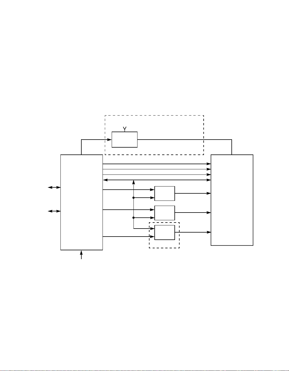
A block diagram of the LSI53C875 is pictured in Figure 1.2.
Figure 1.2 LSI53C875 Chip Block Diagram
PCI
PCI Master and Slave Control Block
External
Memory
Memory
Control
Local
Bus
Memory
Data
FIFO
536 Bytes
SCSI
SCRIPTS
Processor
SCSI FIFO and SCSI Control Block
Operating
Registers
TolerANT Drivers and Receivers
SCSI Bus
Configuration
Registers
SCRIPTS
RAM
The LSI53C875 integrates a high-performance SCSI core, a PCI bus
master DMA core, and the LSI Logic SCSI SCRIPTS processor to meet
the flexibility requirements of SCSI-3 and Ultra SCSI standards. It is
designed to implement multithreaded I/O algorithms with a minimum of
processor intervention, solving the protocol overhead problems of
previous intelligent and nonintelligent adapter designs.
The LSI53C875 is fully supported by the LSI Logic Storage Device
Management System (SDMS™), a software package that supports the
Advanced SCSI Protocol Interface (ASPI) and the ANSI Common
Access Method (CAM). SDMS software provides BIOS and driver
support for hard disk, tape, removable media products, and CD-ROM
under the major PC operating systems.
1-3
Page 18

1.1 Package and Feature Options
The LSI53C875 is available in three versions with different packaging
and feature options. The LSI53C875 is packaged in a 160-pin Plastic
Quad Flat Pack (PQFP). The LSI53C875J is identical to the LSI53C875
with additional pins that support JTAG boundary scan testing. The JTAG
boundary scan signals replace the TESTIN, MAC/_TESTOUT, BIG_LIT/,
and SDIRP1 pins.
The LSI53C875N includes all of the signals in the LSI53C875, with the
addition of the JTAG pins and four additional signals for extended parity
checking and generation. It is packaged in a 208-pin PQFP.
The LSI53C875JB is identical to the LSI53C875J, but is packaged in a
169-pin Ball Grid Array (BGA). The LSI53C875E, LSI53C875JE, and
LSI53C875JBE have been upgraded to include the power management
features.
1.2 Benefits of Ultra SCSI
Ultra SCSI is an extension of the SCSI-3 standard that expands the
bandwidth of the SCSI bus and allows faster synchronous SCSI transfer
rates. When enabled, Ultra SCSI performs 20 megatransfers during an
I/O operation, resulting in approximately twice the synchronous transfer
rates of fast SCSI-2. The LSI53C875 can perform 8-bit, Ultra SCSI
synchronous transfers as fast as 20 Mbytes/s. This advantage is most
noticeable in heavily loaded systems, or large block size requirements,
such as video on-demand and image processing.
An advantage of Ultra SCSI is that it significantly improves SCSI
bandwidth while preserving existing hardware and software investments.
The LSI53C875 is compatible with all existing LSI53C825 and
LSI53C825A software; the only changes required are to enable the chip
to perform synchronous negotiations for Ultra SCSI rates. The
LSI53C875 can use the same board socket as an LSI53C825, with the
addition of an 80 MHz SCLK or enabling the internal SCSI clock doubler
to provide the correct frequency when transferring synchronous SCSI
data at 50 nanosecond transfer rates. Some changes to existing cabling
or system designs may be needed to maintain signal integrity at Ultra
SCSI synchronous transfer rates. These design issues are discussed in
Chapter 2, “Functional Description.”
1-4 General Description
Page 19

1.3 TolerANT®Technology
The LSI53C875 features TolerANT technology, which includes active
negation on the SCSI drivers and input signal filtering on the SCSI
receivers. Active negation actively drives the SCSI Request,
Acknowledge, Data, and Parity signals HIGH rather than allowing them
to be passively pulled up by terminators. Active negation is enabled by
setting bit 7 in the SCSI Test Three (STEST3) register.
TolerANT receiver technology improves data integrity in unreliable
cabling environments, where other devices would be subject to data
corruption. TolerANT receivers filter the SCSI bus signals to eliminate
unwanted transitions, without the long signal delay associated with
RC-type input filters. This improved driver and receiver technology helps
eliminate double clocking of data, the single biggest reliability issue with
SCSI operations. TolerANT technology input signal filtering is a built-in
feature of the LSI53C875 and all LSI Logic fast SCSI devices. On the
LSI53C875, the user may select a filtering period of 30 or 60 ns, with
bit 1 in the SCSI Test Two (STEST2) register.
The benefits of TolerANT technology include increased immunity to noise
when the signal is going HIGH, better performance due to balanced duty
cycles, and improved fast SCSI transfer rates. In addition, TolerANT
SCSI devices do not cause glitches on the SCSI bus at power-up or
power-down, so other devices on the bus are also protected from data
corruption. TolerANT technology is compatible with both the Alternative
One and Alternative Two termination schemes proposed by the
American National Standards Institute.
TolerANT®Technology 1-5
Page 20

1.4 LSI53C875 Benefits Summary
The section provides an overview of the LSI53C875 features and
benefits. It contains information on SCSI Performance, PCI Performance,
Integration, Ease of Use, Flexibility, Reliability, and Testability.
1.4.1 SCSI Performance
To improve SCSI performance, the LSI53C875:
• Includes 4 Kbyte internal RAM for SCRIPTS instruction storage.
• Performs wide, Ultra SCSI synchronous transfers as fast as
40 Mbytes/s.
• Increases SCSI synchronous offset from 8 to 16 levels.
• Supports variable block size and scatter/gather data transfers.
• Performs sustained memory-to-memory DMA transfers faster than
47 Mbytes/s (@ 33 MHz).
• Minimizes SCSI I/O start latency.
• Performs complex bus sequences without interrupts, including
restore data pointers.
• Reduces interrupt service routine overhead through a unique
interrupt status reporting method.
• Performs fast and wide SCSI bus transfers in SE and differential
mode.
– 10 Mbytes/s asynchronous (20 Mbytes/s with Ultra SCSI).
– 20 Mbytes/s synchronous (40 Mbytes/s with Ultra SCSI).
• Supports Load and Store SCRIPTS instructions to increase the
performance of data transfers to and from chip registers.
• Supports target disconnect and later reconnect with no interrupt to
the system processor.
• Supports multithreaded I/O algorithms in SCSI SCRIPTS with fast
I/O context switching.
• Supports expanded Register Move instructions to support additional
arithmetic capability.
• Complies with PCI Bus Power Management Specification
(LSI53C875E) Revision 1.0.
1-6 General Description
Page 21

1.4.2 PCI Performance
To improve PCI performance, the LSI53C875:
• Complies with PCI 2.1 specification.
• Bursts 2, 4, 8, 16, 32, 64, or 128 Dwords across PCI bus.
• Supports 32-bit word data bursts with variable burst lengths.
• Prefetches up to 8 Dwords of SCRIPTS instructions.
• Bursts SCRIPTS opcode fetches across the PCI bus.
• Performs zero wait-state bus master data bursts faster than
110 Mbytes/s (@ 33 MHz).
• Supports PCI Cache Line Size register.
• Supports PCI Write and Invalidate, Read Line, and Read Multiple
commands.
1.4.3 Integration
The following features ease integration of the LSI53C875 into a system:
• 3.3 V/5 V PCI interface.
• Full 32-bit PCI DMA bus master.
• Memory Move instructions allow use as a third-party PCI bus DMA
• High-performance SCSI core.
• Integrated SCRIPTS processor.
1.4.4 Ease of Use
The following features of the LSI53C875 make the device user friendly:
• Up to 1 Mbyte of add-in memory support for BIOS and SCRIPTS
• Direct PCI to SCSI connection.
• Reduced SCSI development effort.
• Easily adapted to the Advanced SCSI Protocol Interface (ASPI) or
LSI53C875 Benefits Summary 1-7
controller.
storage.
the ANSI Common Access Method (CAM), with SDMS software.
Page 22

1.4.5 Flexibility
• Compiler-compatible with existing LSI53C7XX and LSI53C8XX
family SCRIPTS.
• Direct connection to PCI, and SCSI SE and differential buses.
• Development tools and sample SCSI SCRIPTS available.
• Maskable and pollable interrupts.
• Wide SCSI, A or P cable, and up to 16 devices are supported.
• Three programmable SCSI timers: Select/Reselect, Handshake-to-
Handshake, and General Purpose. The time-out period is
programmable from 100 µs to greater than 25.6 seconds.
• SDMS software for complete PC-based operating system support.
• Support for relative jumps.
• SCSI Selected As ID bits for responding with multiple IDs.
The following features increase the flexibility of the LSI53C875:
• High level programming interface (SCSI SCRIPTS).
• Programs local memory and bus Flash memory.
• Big/little endian support.
• Selectable 88 or 536 byte DMA FIFO for backward compatibility.
• Tailored SCSI sequences execute from main system RAM or internal
SCRIPTS RAM.
• Flexible programming interface to tune I/O performance or to adapt
to unique SCSI devices.
• Support for changes in the logical I/O interface definition.
• Low level access to all registers and all SCSI bus signals.
• Fetch, Master, and Memory Access control pins.
• Separate SCSI and system clocks.
• SCSI clock doubler bits enable Ultra SCSI transfer rates with a
40 MHz SCSI clock.
• Selectable IRQ pin disable bit.
• 32 additional scratch pad registers.
• Ability to route system clock to SCSI clock.
1-8 General Description
Page 23

1.4.6 Reliability
The following features enhance the reliability of the LSI53C875:
• 2 kV ESD protection on SCSI signals.
• Typical 300 mV SCSI bus hysteresis.
• Protection against bus reflections due to impedance mismatches.
• Controlled bus assertion times (reduces RFI, improves reliability, and
eases FCC certification).
• Latch-up protection greater than 150 mA.
• Voltage feed-through protection (minimum leakage current through
SCSI pads).
• A high proportion (> 25%) of pins are power and ground.
• Power and ground isolation of I/O pads and internal chip logic.
• TolerANT technology which provides:
– Active negation of SCSI Data, Parity, Request, and Acknowledge
signals for improved fast SCSI transfer rates.
– Input signal filtering on SCSI receivers improves data integrity,
even in noisy cabling environments.
• JTAG Boundary scan support (LSI53C875J, LSI53C875JB,
LSI53C875N only).
1.4.7 Testability
• Extended PCI parity checking and generation (LSI53C875N only).
• Extended SCSI parity checking.
The following features enhance the testability of the LSI53C875:
• Access to all SCSI signals through programmed I/O.
• SCSI loopback diagnostics.
• SCSI bus signal continuity checking.
• Support for single step mode operation.
• Test mode (AND tree) to check pin continuity to the board (most
package options).
• JTAG Boundary scan support (LSI53C875J, LSI53C875JB,
LSI53C875N only).
LSI53C875 Benefits Summary 1-9
Page 24

1-10 General Description
Page 25

Chapter 2
Functional Description
Chapter 2 is divided into the following sections:
• Section 2.1, “SCSI Functional Description”
• Section 2.2, “Designing an Ultra SCSI System”
• Section 2.3, “Prefetching SCRIPTS Instructions”
• Section 2.4, “External Memory Interface”
• Section 2.5, “PCI Cache Mode”
• Section 2.6, “Power Management”
2.1 SCSI Functional Description
The LSI53C875 is composed of three functional blocks: the SCSI Core,
the DMA Core, and the SCRIPTS Processor. The LSI53C875 is fully
supported by SDMS software, a complete software package that
supports the LSI Logic product line of SCSI processors and controllers.
The PCI Bus Power Management support (LSI53C875E) is discussed
Section 2.6, “Power Management.”
2.1.1 SCSI Core
The SCSI core supports the 8-bit or 16-bit data bus. It supports Ultra
SCSI synchronous transfer rates up to 40 Mbytes/s, SCSI synchronous
transfer rates up to 20 Mbytes/s, and asynchronous transfer rates up to
10 Mbytes/s on a 16-bit wide SCSI bus. The SCSI core can be
programmed with SCSI SCRIPTS, making it easy to “fine tune” the
system for specific mass storage devices or SCSI-3 requirements.
LSI53C875/875E PCI to Ultra SCSI I/O Processor 2-1
Page 26

2.1.2 DMA Core
The SCSI core offers low level register access or a high level control
interface. Like first generation SCSI devices, the LSI53C875 SCSI core
can be accessed as a register oriented device. The ability to sample
and/or assert any signal on the SCSI bus can be used in error recovery
and diagnostic procedures. In support of loopback diagnostics, the SCSI
core may perform a self-selection and operate as both an initiator and a
target.
The LSI53C875 SCSI core is controlled by the integrated SCRIPTS
processor through a high level logical interface. Commands controlling
the SCSI core are fetched out of the main host memory or local memory.
These commands instruct the SCSI core to Select, Reselect, Disconnect,
Wait for a Disconnect, Transfer Information, Change Bus Phases and, in
general, implement all aspects of the SCSI protocol. The SCRIPTS
processor is a special high speed processor optimized for SCSI protocol.
The DMA core is a bus master DMA device that attaches directly to the
industry standard PCI Bus. The DMA core is tightly coupled to the SCSI
core through the SCRIPTS processor, which supports uninterrupted
scatter/gather memory operations.
The LSI53C875 supports 32-bit memory and automatically supports
misaligned DMA transfers. A 536-byte FIFO allows the LSI53C875 to
support 2, 4, 8, 16, 32, 64, or 128 longword bursts across the PCI bus
interface.
2.1.3 SCRIPTS Processor
The SCSI SCRIPTS processor allows both DMA and SCSI commands
to be fetched from host memory or internal SCRIPTS RAM. Algorithms
written in SCSI SCRIPTS control the actions of the SCSI and DMA cores
and are executed from 32-bit system RAM. The SCRIPTS processor
executes complex SCSI bus sequences independently of the host CPU.
The SCRIPTS processor can begin a SCSI I/O operation in
approximately 500 ns. This compares with 2–8 ms required for traditional
intelligent host adapters. Algorithms may be designed to tune SCSI bus
performance, to adjust to new bus device types (such as scanners,
communication gateways, etc.), or to incorporate changes in the SCSI-2
2-2 Functional Description
Page 27

or SCSI-3 logical bus definitions without sacrificing I/O performance.
SCSI SCRIPTS are hardware independent, so they can be used
interchangeably on any host or CPU system bus.
2.1.4 Internal SCRIPTS RAM
The LSI53C875 has 4 Kbyte (1024 x 32 bits) of internal, general purpose
RAM. The RAM is designed for SCRIPTS program storage, but is not
limited to this type of information. When the chip fetches SCRIPTS
instructions or Table Indirect information from the internal RAM, these
fetches remain internal to the chip and do not use the PCI bus. Other
types of access to the RAM by the LSI53C875 use the PCI bus, as if
they were external accesses. The MAD5 pin enables the 4 Kbyte internal
RAM. To disable the internal RAM, connect a 4.7 kΩ resistor between
the MAD5 pin and V
The RAM can be relocated by the PCI system BIOS anywhere in 32-bit
address space. The RAM Base Address register in PCI configuration
space contains the base address of the internal RAM. This register is
similar to the ROM Base Address register in PCI configuration space. To
simplify loading of SCRIPTS instructions, the base address of the RAM
will appear in the Scratch Register B (SCRATCHB) register when bit 3 of
the Chip Test Two (CTEST2) register is set. The RAM is byte accessible
from the PCI bus and is visible to any bus mastering device on the bus.
External accesses to the RAM (by the CPU) follow the same timing
sequence as a standard slave register access, except that the target
wait-states required drop from 5 to 3.
SS
.
A complete set of development tools is available for writing custom
drivers with SCSI SCRIPTS. For more information on the SCSI SCRIPTS
instructions supported by the LSI53C875, see Chapter 6, “Instruction Set
of the I/O Processor.”
2.1.5 SDMS Software: The Total SCSI Solution
For users who do not need to develop custom drivers, LSI Logic provides
a total SCSI solution in PC environments with the SDMS. SDMS
software provides BIOS driver support for hard disk, tape, and removable
media peripherals for the major PC-based operating systems.
SCSI Functional Description 2-3
Page 28

SDMS software includes a SCSI BIOS to manage all SCSI functions
related to the device. It also provides a series of SCSI device drivers that
support most major operating systems. SDMS software supports a
multithreaded I/O application programming interface (API) for user
developed SCSI applications. SDMS software supports both the ASPI
and CAM SCSI software specifications.
2.2 Designing an Ultra SCSI System
Migrating an existing SE SCSI design from SCSI-2 to Ultra SCSI requires
minor software modifications as well as consideration for some hardware
design guidelines. Since Ultra SCSI is based on existing SCSI standards,
it can use existing software programs as long as the software is able to
negotiate for Ultra SCSI synchronous transfer rates.
In the area of hardware, the primary area of concern in SE systems is to
maintain signal integrity at high data transfer rates. To assure reliable
operation at Ultra SCSI transfer speeds, follow the system design
parameters recommended in the SCSI-3 Ultra Parallel Interface
standard. Chapter 7, “Instruction Set of the I/O Processor,” contains Ultra
SCSI timing information. In addition to the guidelines in the draft
standard, make the following software and hardware adjustments to
accommodate Ultra SCSI transfers:
• Set the Ultra Enable bit to enable Ultra SCSI transfers.
• Set the TolerANT Enable bit, bit 7 in the SCSI Test Three (STEST3)
register whenever the Ultra Enable bit is set.
• Do not extend the SREQ/SACK filtering period with SCSI Test Two
(STEST2), bit 1.
2.2.1 Using the SCSI Clock Doubler
The LSI53C875 can double the frequency of a 40–50 MHz SCSI clock,
allowing the system to perform Ultra SCSI transfers in systems that do
not have 80 MHz clock input. This option is user selectable with bit
settings in the SCSI Test One (STEST1), SCSI Test Three (STEST3),
and SCSI Control Three (SCNTL3) registers. At power-on or reset, the
doubler is disabled and powered down. Follow these steps to use the
clock doubler:
2-4 Functional Description
Page 29

Step 1. Set the SCLK Doubler Enable bit (SCSI Test One (STEST1),
bit 3).
Step 2. Wait 20 µs.
Step 3. Halt the SCSI clock by setting the Halt SCSI Clock bit (SCSI
Test Three (STEST3), bit 5).
Step 4. Set the clock conversion factor using the SCF and CCF fields
in the SCSI Control Three (SCNTL3) register.
Step 5. Set the SCLK Doubler Select bit (SCSI Test One (STEST1),
bit 2).
Step 6. Clear the Halt SCSI Clock bit.
2.3 Prefetching SCRIPTS Instructions
When enabled by setting the Prefetch Enable bit in the DMA Control
(DCNTL) register, the prefetch logic in the LSI53C875 fetches 8 Dwords
of instructions. The prefetch logic automatically determines the maximum
burst size that it can perform, based on the burst length as determined
by the values in the DMA Mode (DMODE) register. If the unit cannot
perform bursts of at least four Dwords, it disables itself. While the
LSI53C875 is prefetching SCRIPTS instructions, the PCI Cache Line
Size register value does not have any effect and the Read Line, Read
Multiple, and Write and Invalidate commands are not used.
The LSI53C875 may flush the contents of the prefetch unit under certain
conditions, listed below, to ensure that the chip always operates from the
most current version of the software. When one of these conditions
apply, the contents of the prefetch unit are automatically flushed.
• On every Memory Move instruction. The Memory Move instruction is
often used to place modified code directly into memory. To make
sure that the chip executes all recent modifications, the prefetch unit
flushes its contents and loads the modified code every time an
instruction is issued. To avoid inadvertently flushing the prefetch unit
contents, use the No Flush option for all Memory Move operations
that do not modify code within the next 8 Dwords. For more
information on this instruction, refer to Chapter 6, “Instruction Set of
the I/O Processor.”
Prefetching SCRIPTS Instructions 2-5
Page 30

• On every Store instruction. The Store instruction may also be used
to place modified code directly into memory. To avoid inadvertently
flushing the prefetch unit contents use the No Flush option for all
Store operations that do not modify code within the next 8 Dwords.
• On every write to the DMA SCRIPTS Pointer (DSP).
• On all Transfer Control instructions when the transfer conditions are
met. This is necessary because the next instruction to execute is not
the sequential next instruction in the prefetch unit.
• When the Prefetch Flush bit (DMA Control (DCNTL), bit 6) is set. The
unit flushes whenever this bit is set. The bit is self-clearing.
2.3.1 Opcode Fetch Burst Capability
Setting the Burst Opcode Fetch Enable bit in the DMA Mode (DMODE)
register (0x38) causes the LSI53C875 to burst in the first two longwords
of all instruction fetches. If the instruction is a Memory-to-Memory Move,
the third longword is accessed in a separate ownership. If the instruction
is an indirect type, the additional longword is accessed in a subsequent
bus ownership. If the instruction is a Table Indirect Block Move, the chip
uses two accesses to obtain the four longwords required, in two bursts
of two longwords each.
Note: This feature is only useful if prefetching is disabled.
2.4 External Memory Interface
The LSI53C875 supports up to one megabyte of external memory in
binary increments from 16 Kbytes, to allow the use of expansion ROM
for add-in PCI cards. The device also supports Flash ROM updates
through the add-in interface and the GPIO4 pin (used to control VPP, the
power supply for programming external memory). This interface is
designed for low speed operations such as downloading instruction code
from ROM. It is not intended for dynamic activities such as executing
instructions.
System requirements include the LSI53C875, two or three external 8-bit
address holding registers (HCT273 or HCT374), and the appropriate
memory device. The 4.7 kΩ pull-down resistors on the MAD bus require
HC or HCT external components to be used. If in-system Flash ROM
2-6 Functional Description
Page 31

updates are required, a 7406 (high voltage open collector inverter), an
MTD4P05, and several passive components are also needed. The
memory size and speed is determined by pull-down resistors on the
8-bit bidirectional memory bus at power-up. The LSI53C875 senses this
bus shortly after the release of the Reset signal and configures the ROM
Base Address register and the memory cycle state machines for the
appropriate conditions.
The external memory interface works with a variety of ROM sizes and
speeds. An example set of interface drawings is in Appendix B, “External
Memory Interface Diagram Examples.”
The LSI53C875 supports a variety of sizes and speeds of expansion
ROM, using pull-down resistors on the MAD[3:0] pins. The encoding of
pins MAD[3:1] allows the user to define how much external memory is
available to the LSI53C875. Table 2.1 shows the memory space
associated with the possible values of MAD[3:1]. The MAD[3:1] pins are
fully defined in Chapter 4, “Signal Descriptions.”
Table 2.1 External Memory Support
MAD[3:1] Available Memory Space
000 16 Kbytes
001 32 Kbytes
010 64 Kbytes
011 128 Kbytes
100 256 Kbytes
101 512 Kbytes
110 1024 Kbytes
111 No external memory present
To use one of the configurations mentioned above in a host adapter
board design, put 4.7 kΩ pull-down resistors on the MAD pins
corresponding to the available memory space. For example, to connect
to a 32 Kbytes external ROM, use pull-downs on MAD[3] and MAD[2]. If
the external memory interface is not used, then no external resistors are
External Memory Interface 2-7
Page 32

necessary since there are internal pull-ups on the MAD bus. The internal
pull-up resistors are disabled when external pull-down resistors are
detected, to reduce current drain.
The LSI53C875 allows the system to determine the size of the available
external memory using the Expansion ROM Base Address register in
PCI configuration space. For more information on how this works, refer
to the PCI specification or the Expansion ROM Base Address register
description in Chapter 3, “PCI Functional Description.”
MAD[0] is the slow ROM pin. When pulled down, it enables two extra
clock cycles of data access time to allow use of slower memory devices.
The external memory interface also supports updates to Flash memory.
The 12 V power supply for Flash memory, V
with the GPIO4 pin and the GPIO4 control bit. For more information on
the GPIO4 pin, refer to Chapter 4, “Signal Descriptions.”
2.5 PCI Cache Mode
The LSI53C875 supports the PCI specification for an 8-bit Cache Line
Size register located in PCI configuration space. The Cache Line Size
register provides the ability to sense and react to nonaligned addresses
corresponding to cache line boundaries. In conjunction with the Cache
Line Size register, the PCI commands Read Line, Read Multiple, and
Write and Invalidate are each software enabled or disabled to allow the
user full flexibility in using these commands. For more information on PCI
cache mode operations, refer to Chapter 3, “PCI Functional Description.”
, is enabled and disabled
PP
2.5.1 Load/Store Instructions
The LSI53C875 supports the Load and Store instruction type, which
simplifies the movement of data between memory and the internal chip
registers. It also enables the chip to transfer bytes to addresses relative
to the Data Structure Address (DSA) register. For more information on
the Load and Store instructions, refer to Chapter 6, “Instruction Set of the
I/O Processor.”
2-8 Functional Description
Page 33

2.5.2 3.3 V/5 V PCI Interface
The LSI53C875 can attach directly to a 3.3 V ora5VPCIinterface, due
to separate V
be used on the universal board recommended by the PCI Special
Interest Group.
pins for the PCI bus drivers. This allows the devices to
DD
2.5.3 Additional Access to General Purpose Pins
The LSI53C875 can access the GPIO0 and GPIO1 general purpose pins
through register bits in the PCI configuration space, instead of using the
General Purpose Pin Control (GPCNTL) register in the operating register
space to control these pins. In the LSI Logic SDMS software, the
configuration bits control pins as the clock and data lines, respectively.
To access the GPIO[1:0] pins through the configuration space, connect
a 4.7 kΩ resistor between the MAD[7] pin and VSS. MAD[7] contains an
internal pull-up that is sensed shortly after chip reset. If the pin is sensed
high, GPIO[1:0] access is disabled; if it is low, GPIO[1:0] access is
enabled. Additionally, if GPIO[1:0] access has been enabled through the
MAD[7] pin and if GPIO0 and/or GPIO1 are sensed low after chip reset,
GPIO[1:0] access is disabled. If GPIO[1:0] access through configuration
space is enabled, the GPIO0 and GPIO1 pins cannot be controlled from
the General Purpose Pin Control (GPCNTL) and General Purpose
(GPREG) registers, but are observable from the General Purpose
(GPREG) register. When GPIO[1:0] access is enabled, the Serial
Interface Control register at configuration addresses 0x34–0x35 controls
the GPIO0 and GPIO1 pins. For more information on GPIO[1:0] access,
refer to the Serial Interface Control register description in Chapter 3, “PCI
Functional Description.” For more information on the GPIO pins, see
Chapter 4, “Signal Descriptions.” This does not apply to the LSI53C875E.
Note: The LSI Logic SDMS software controls the GPIO0 and
GPIO1 pins using the General Purpose Pin Control
(GPCNTL) and General Purpose (GPREG) registers.
Therefore,if using SDMS software,do not connect a 4.7 kΩ
resistor between MAD[7] and Vss.
PCI Cache Mode 2-9
Page 34

2.5.4 JTAG Boundary Scan Testing
The LSI53C875J/LSI53C875N/LSI53C875JB include support for JTAG
boundary scan testing in accordance with the IEEE 1149.1 specification
with one exception, which is discussed in this section. The device
accepts all required boundary scan instructions, including the optional
CLAMP, HIGH-Z, and IDCODE instructions.
The LSI53C875J/LSI53C875N/LSI53C875JB use an 8-bit instruction
register to support all boundary scan instructions. The data registers
included in the device are the Boundary Data register, the IDCODE
register, and the Bypass register. This device can handle a 10 MHz TCK
frequency for TDO and TDI.
Due to design constraints, the RST/ pin (system reset) always 3-states
the SCSI pins when it is asserted. Boundary scan logic does not control
this action, and this is not compliant with the specification. There are two
solutions that resolve this issue:
1. Use the RST/ pin as a boundary scan compliance pin. When the pin
is deasserted, the device is boundary scan compliant and when
asserted, the device is noncompliant. To maintain compliance the
RST/ pin must be driven high.
2. When RST/ is asserted during boundary scan testing the expected
output on the SCSI pins must be a HIGH-Z condition, and not what
is contained in the boundary scan data registers for the SCSI pin
output cells.
Because of package limitations, the LSI53C875J/LSI53C875JB replaces
the TESTIN, MAC/_TESTOUT, BIG_LIT/, and SDIRP1 signals with the
JTAG boundary scan signals. The LSI53C875N includes support for
these signals in addition to the JTAG pins.
2.5.5 Big and Little Endian Support
The LSI53C875/LSI53C875N supports both big and little endian byte
ordering through pin selection. The LSI53C875J/LSI53C875JB operatein
little endian mode only (the BIG_LIT pin is replaced by one of the JTAG
boundary scan signals). In big endian mode, the first byte of an aligned
SCSI to PCI transfer is routed to lane three and succeeding transfers are
routed to descending lanes. This mode of operation also applies to data
transfers over the add-in ROM interface. The byte of data accessed at
2-10 Functional Description
Page 35

location 0x0000 from memory is routed to lane three, and the data at
location 0x0003 is routed to byte lane 0. In little endian mode, the first
byte of an aligned SCSI to PCI transfer is routed to lane zero and
succeeding transfers are routed to ascending lanes. This mode of
operation also applies to the add-in ROM interface. The byte of data
accessed at location 0x0000 from memory is routed to lane zero, and
the data at location 0x0003 is routed to byte lane 3.
The Big_Lit pin gives the LSI53C875 the flexibility of operating with either
big or little endian byte orientation. Internally, in either mode, the actual
byte lanes of the DMA FIFO and registers are not modified. The
LSI53C875 supports slave accesses in big or little endian mode.
When a Dword is accessed, no repositioning of the individual bytes is
necessary since Dwords are addressed by the address of the least
significant byte. SCRIPTS always uses Dwords in 32-bit systems, so
compatibility is maintained between systems using different byte
orientations. When less than a Dword is accessed, individual bytes must
be repositioned. Internally, the LSI53C875 adjusts the byte control logic
of the DMA FIFO and register decodes to access the appropriate byte
lanes. The registers always appear on the same byte lane, but the
address of the register is repositioned.
Big/little endian mode selection has the most effect on individual byte
access. Internally, the LSI53C875 adjusts the byte control logic of the
DMA FIFO and register decodes to enable the appropriate byte lane. The
registers always appear on the same byte lane, but the address of the
register is repositioned.
Data to be transferred between system memory and the SCSI bus
always starts at address zero and continues through address ‘n’ – there
is no byte ordering in the chip. The first byte in from the SCSI bus goes
to address 0, the second to address 1, etc. Going out onto the SCSI bus,
address zero is the first byte out on the SCSI bus, address 1 is the
second byte, etc. The only difference is that in a little endian system,
address 0 is on byte lane 0, and in big endian mode address zero is on
byte lane 3.
Correct SCRIPTS are generated if the SCRIPTS compiler is run on a
system that has the same byte ordering as the target system. Any
SCRIPTS patching in memory must patch the instruction with the byte
ordering that the SCRIPTS processor expects.
PCI Cache Mode 2-11
Page 36

Software drivers for the LSI53C875 should access registers by their
logical name (that is, SCNTL0) rather than by their address. The logical
name should be equated to the register’s big endian address in big
endian mode (SCNTL0 = 0x03), and its little endian address in little
endian mode (SCNTL0 = 0x00). This way, there is no change to the
software when moving from one mode to the other; only the equate
statement setting the operating modes needs to be changed.
Addressing of registers from within a SCRIPTS instruction is independent
of bus mode. Internally, the LSI53C875 always operates in little endian
mode.
2.5.6 Loopback Mode
The LSI53C875 loopback mode allows testing of both initiator and target
functions and, in effect, lets the chip communicate with itself. When the
Loopback Enable bit is set in the SCSI Test One (STEST1) register, the
LSI53C875 allows control of all SCSI signals whether the chip is
operating in initiator or target mode. For more information on this mode
of operation refer to the SCSI SCRIPTS Processors Programming Guide.
2.5.7 Parity Options
The LSI53C875 implements a flexible parity scheme that allows control
of the parity sense, allows parity checking to be turned on or off, and has
the ability to deliberately send a byte with bad parity over the SCSI bus
to test parity error recovery procedures. Table 2.2 defines the bits that
are involved in parity control and observation. Table 2.3 describes the
parity control function of the Enable Parity Checking and Assert SCSI
Even Parity bits in the SCSI Control Zero (SCNTL0) register. Table 2.4
describes the options available when a parity error occurs.
The LSI53C875N has four additional parity pins for checking incoming
data on the PCI bus. These pins are assigned to each byte of the PCI
address/data bus, and work in addition to the PAR (PCI parity) pin. In
PCI master read or slave write operations, each byte of incoming data
on the PCI bus is checked against its corresponding parity line, in
addition to the normal parity checking against the PCI PAR signal. In PCI
master write or slave read operations, parity is generated for each byte.
This extra parity checking is always enabled for the LSI53C875N. The
host system must support these pins. This feature is not register
selectable. A parity error on any Byte Parity pin for PCI master read or
2-12 Functional Description
Page 37

slave write operations causes a fatal DMA interrupt; SCRIPTS stops
running. Mask this interrupt with the EBPE Interrupt Enable bit, bit 1 in
the DMA Interrupt Enable (DIEN) register. These additional parity pins in
no way affect the generation or checking of the PCI specified parity line.
Table 2.2 Bits Used for Parity Control and Generation
BIt Name Location Description
Assert SATN/ on Parity
Errors
Enable Parity Checking SCSI Control
Assert Even SCSI Parity SCSI Control
Disable Halt on SATN/
or a Parity Error (Target
Mode Only)
Enable Parity Error
Interrupt
Parity Error SCSI Interrupt
Status of SCSI Parity
Signal
SCSI SDP1 Signal SCSI Status Two
SCSI Control
Zero (SCNTL0),
Bit 1
Zero (SCNTL0),
Bit 3
One (SCNTL1),
Bit 2
SCSI Control
One (SCNTL1),
Bit 5
SCSI Interrupt
Enable Zero
(SIEN0), Bit 0
Status Zero
(SIST0), Bit 0
SCSIStatus Zero
(SSTAT0), Bit 0
(SSTAT2), Bit 0
When this bit is set, the LSI53C875 automatically
asserts the SATN/ signal upon detection of a parity
error. SATN/ is only asserted in initiator mode.
Enables the LSI53C875 to check for parity errors. The
LSI53C875 checks for odd parity. This bit also checks
for parity errors on thefour additional parity pins on the
LSI53C875N.
DeterminestheSCSIparity sensegeneratedbythe
LSI53C875 to the SCSI bus.
Causes the LSI53C875 not to halt operations when a
parity error is detected in target mode.
Determines whether the LSI53C875 generates an
interrupt when it detects a SCSI parity error.
This status bit is set whenever the LSI53C875 has
detected a parity error on the SCSI bus.
This status bit represents the active HIGH current state
of the SCSI SDP0 parity signal.
This bit represents the active HIGH current state of the
SCSI SDP1 parity signal.
Latched SCSI Parity SCSI Status Two
Master Parity Error
Enable
(SSTAT2), Bit 3
and SCSI Status
One (SSTAT1),
Bit 3
Chip Test Four
(CTEST4), Bit 3
PCI Cache Mode 2-13
These bits reflect the SCSI odd parity signal
corresponding to the data latched into the SCSI Input
Data Latch (SIDL) register.
Enables parity checking during master data phases.
Page 38

Table 2.2 Bits Used for Parity Control and Generation (Cont.)
BIt Name Location Description
Master Data Parity Error DMA Status
Master Data Parity Error
Interrupt Enable
Extended Byte Parity
Error Interrupt Enable
(LSI53C875N only)
(DSTAT), Bit 6
DMA Interrupt
Enable (DIEN),
Bit 6
DMA Interrupt
Enable (DIEN),
Bit 1
Set when the LSI53C875 as a master detects that a
target device has signaled a parity error during a data
phase.
By clearing this bit, a Master Data Parity Error will not
cause IRQ/ to be asserted, but the status bit will be set
in the DMA Status (DSTAT) register.
By clearing this bit, an Extended Byte Parity Error will
not cause IRQ/ to be asserted, but the status bit will be
set in the DMA Status (DSTAT) register.
Table 2.3 SCSI Parity Control
EPC AESP Description
0 0 Does not check for parity errors. Parity is generated when sending
0 1 Does not check for parity errors. Parity is generated when sending
1 0 Checks for odd parity on SCSI data received. Parity is generated
1 1 Checks for odd parity on SCSI data received. Parity is generated
SCSI data. Asserts odd parity when sending SCSI data.
SCSI data. Asserts even parity when sending SCSI data.
when sending SCSI data. Asserts odd parity when sending SCSI
data.
when sending SCSI data. Asserts even parity when sending SCSI
data.
1. Key:
EPC = Enable Parity Checking (bit 3, SCSI Control Zero (SCNTL0)).
ASEP = Assert SCSI Even Parity (bit 2, SCSI Control One (SCNTL1)).
2. This table only applies when the Enable Parity Checking bit is set.
2-14 Functional Description
Page 39
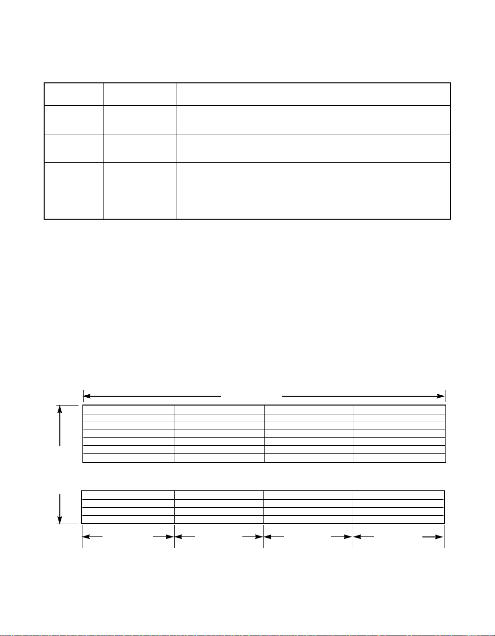
Table 2.4 SCSI Parity Errors and Interrupts
DPH PAR Description
0 0 Halts when a parity error occurs in target or initiator mode and does
0 1 Halts when a parity error occurs in target mode and generates an
1 0 Does not halt in target mode when a parity error occurs until the
1 1 Does not halt in target mode when a parity error occurs until the
Key:
DHP = Disable Halt on SATN/ or Parity Error (bit 5, SCSI Control One (SCNTL1).
PAR = Parity Error (bit 0, SCSI Interrupt Enable One (SIEN1).
not generate an interrupt.
interrupt in the target or initiator mode.
end of the transfer. An interrupt is not generated.
end of the transfer. An interrupt is generated.
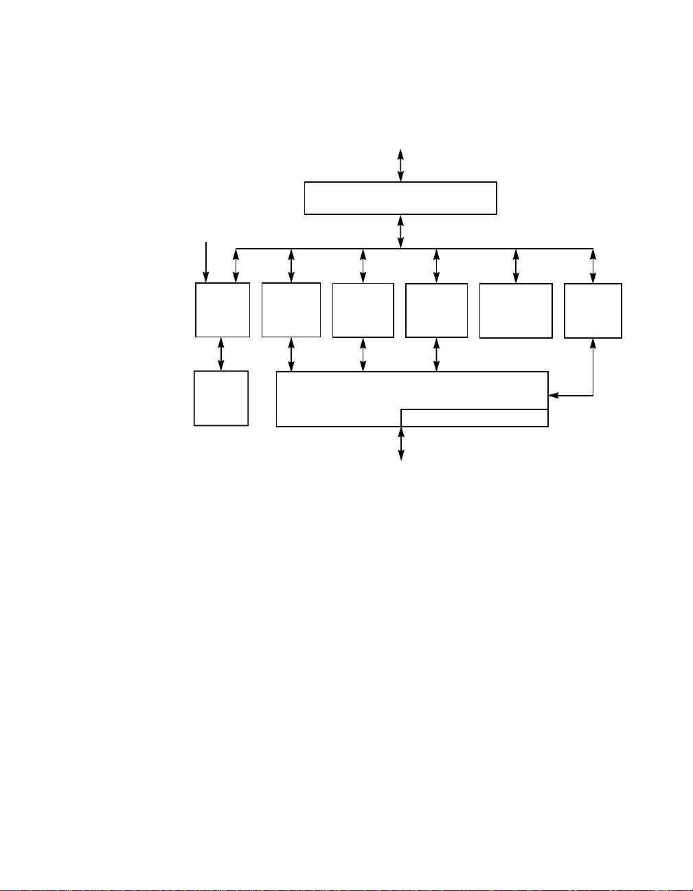
2.5.8 DMA FIFO
The DMA FIFO is 4 bytes wide by 134 transfers deep. The DMA FIFO
is illustrated in Figure 2.1. To assure compatibility with older products in
the LSI53C8XX family, the DMA FIFO size may be set to 88 bytes by
setting the DMA FIFO Size bit, bit 5 in the Chip Test Five (CTEST5)
register.
Figure 2.1 DMA FIFO Sections
32 Bytes Wide
134
Transfers
Deep
.
.
.
8 Bits
Byte Lane 3
PCI Cache Mode 2-15
8 Bits
Byte Lane 2
8 Bits
Byte Lane 1
Byte Lane 0
8 Bits
.
.
.
Page 40
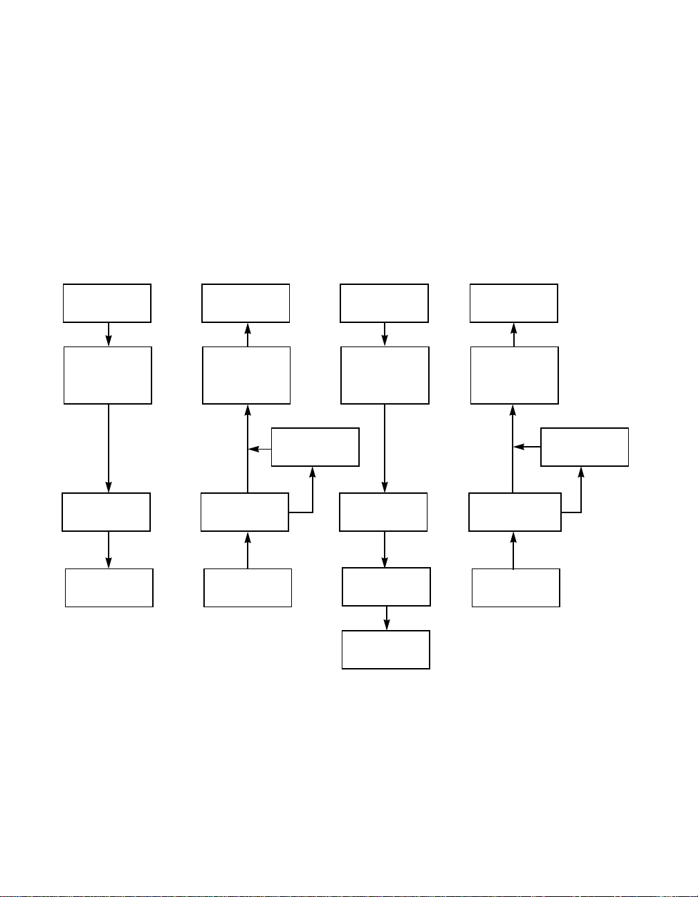
2.5.8.1 Data Paths
The data path through the LSI53C875 is dependent on whether data is
being moved into or out of the chip, and whether SCSI data is being
transferred asynchronously or synchronously.
Figure 2.2 shows how data is moved to/from the SCSI bus in each of the
different modes.
Figure 2.2 LSI53C875 Host Interface Data Paths
Asynchronous
SCSI Send
PCI Interface
DMA FIFO
(32 Bits x 16)
SODL Register
SCSI Interface
Asynchronous
SCSI Receive
PCI Interface
DMA FIFO
(32 Bits x 16)
SIDL Register
SCSI Interface
SWIDE Register
Synchronous
SCSI Send
PCI Interface
DMA FIFO
(32 Bits x 16)
SODL Register
SODR Register SCSI Interface
SCSI Interface
Synchronous
SCSI Receive
PCI Interface
DMA FIFO
(32 Bits x 16)
SCSI FIFO
(8 or 16 Bits x 16)
SWIDE Register
2-16 Functional Description
Page 41

The following steps determine if any bytes remain in the data path when
the chip halts an operation:
Asynchronous SCSI Send –
Step 1. If the DMA FIFO size is set to 88 bytes, look at the DMA FIFO
(DFIFO) and DMA Byte Counter (DBC) registers and calculate
if there are bytes left in the DMA FIFO. To make this calculation,
subtract the seven least significant bits of the DBC register from
the 7-bit value of the DFIFO register. AND the result with 0x7F
for a byte count between 0 and 88.
If the DMA FIFO size is set to 536 bytes (bit 5 of the Chip Test
Five (CTEST5) register), subtract the 10 least significant bits of
the DMA Byte Counter (DBC) register from the 10-bit value of
the DMA FIFO Byte Offset Counter, which consists of bits [1:0]
in the Chip Test Five (CTEST5) register and bits [7:0] of the
DMA FIFO (DFIFO) register. AND the result with 0x3FF for a
byte count between 0 and 536.
Step 2. Read bit 5 in the SCSI Status Zero (SSTAT0) and SCSI Status
Two (SSTAT2) registers to determine if any bytes are left in the
SCSI Output Data Latch (SODL) register. If bit 5 is set in the
SSTAT0 or SSTAT2 register, then the least significant byte or
the most significant byte in the SODL register is full,
respectively. Checking this bit also reveals bytes left in the
SODL register from a Chained Move operation with an odd byte
count.
Synchronous SCSI Send –
Step 1. If the DMA FIFO size is set to 88 bytes, look at the DMA FIFO
(DFIFO) and DMA Byte Counter (DBC) registers and calculate
if there are bytes left in the DMA FIFO. To make this calculation,
subtract the seven least significant bits of the DBC register from
the 7-bit value of the DFIFO register. AND the result with 0x7F
for a byte count between 0 and 88.
If the DMA FIFO size is set to 536 bytes (bit 5 of the Chip Test
Five (CTEST5) register), subtract the 10 least significant bits of
the DMA Byte Counter (DBC) register from the 10-bit value of
PCI Cache Mode 2-17
Page 42

the DMA FIFO Byte Offset Counter, which consists of bits [1:0]
in the CTEST5 register and bits [7:0] of the DMA FIFO register.
AND the result with 0x3FF for a byte count between 0 and 536.
Step 2. Read bit 5 in the SCSI Status Zero (SSTAT0) and SCSI Status
Two (SSTAT2) registers to determine if any bytes are left in the
SCSI Output Data Latch (SODL) register. If bit 5 is set in the
SSTAT0 or SSTAT2 register, then the least significant byte or
the most significant byte in the SODL register is full,
respectively. Checking this bit also reveals bytes left in the
SODL register from a Chained Move operation with an odd byte
count.
Step 3. Read bit 6 in the SCSI Status Zero (SSTAT0) and SCSI Status
Two (SSTAT2) registers to determine if any bytes are left in the
SODR register. If bit 6 is set in the SSTAT0 or SSTAT2 register,
then the least significant byte or the most significant byte in the
SODR register is full, respectively.
Asynchronous SCSI Receive –
Step 1. If the DMA FIFO size is set to 88 bytes, look at the DMA FIFO
(DFIFO) and DMA Byte Counter (DBC) registers and calculate
if there are bytes left in the DMA FIFO. To make this calculation,
subtract the seven least significant bits of the DBC register from
the 7-bit value of the DFIFO register. AND the result with 0x7F
for a byte count between 0 and 88.
If the DMA FIFO size is set to 536 bytes (using bit 5 of the Chip
Test Five (CTEST5) register), subtract the 10 least significant
bits of the DMA Byte Counter (DBC) register from the 10-bit
value of the DMA FIFO Byte Offset Counter, which consists of
bits [1:0] in the CTEST5 register and bits [7:0] of the DMA FIFO
register. AND the result with 0x3FF for a byte count between
0 and 536.
Step 2. Read bit 7 in the SCSI Status Zero (SSTAT0) and SCSI Status
Two (SSTAT2) register to determine if any bytes are left in the
SCSI Input Data Latch (SIDL) register. If bit 7 is set in the
SSTAT0 or SSTAT2, then the least significant byte or the most
significant byte is full, respectively.
2-18 Functional Description
Page 43

Step 3. If any wide transfers have been performed using the Chained
Move instruction, read the Wide SCSI Receive bit (SCSI
Control Two (SCNTL2), bit 0) to determine whether a byte is left
in the SCSI Wide Residue (SWIDE) register.
Synchronous SCSI Receive –
Step 1. If the DMA FIFO size is set to 88 bytes, subtract the seven
least significant bits of the DMA Byte Counter (DBC) register
from the 7-bit value of the DMA FIFO (DFIFO) register. AND
the result with 0x7F for a byte count between 0 and 88.
If the DMA FIFO size is set to 536 bytes (using bit 5 of the Chip
Test Five (CTEST5) register), subtract the 10 least significant
bits of the DMA Byte Counter (DBC) register from the 10-bit
value of the DMA FIFO Byte Offset Counter, which consists of
bits [1:0] in the CTEST5 register and bits [7:0] of the DMA FIFO
register. AND the result with 0x3FF for a byte count between
0 and 536.
Step 2. Read bits [7:4] of the SCSI Status One (SSTAT1) register and
bit 4 of the SCSI Status Two (SSTAT2) register, the binary
representation of the number of valid bytes in the SCSI FIFO,
to determine if any bytes are left in the SCSI FIFO.
Step 3. If any wide transfers have been performed using the Chained
Move instruction, read the Wide SCSI Receive bit (SCSI
Control Two (SCNTL2), bit 0) to determine whether a byte is left
in the SCSI Wide Residue (SWIDE) register.
2.5.9 SCSI Bus Interface
The LSI53C875 supports both SE and differential operation.
All SCSI signals are active low. The LSI53C875 contains the SE output
drivers and can be connected directly to the SCSI bus. Each output is
isolated from the power supply to ensure that a powered down
LSI53C875 has no effect on an active SCSI bus (CMOS “voltage
feed-through” phenomena). TolerANT technology provides signal filtering
at the inputs of SREQ/ and SACK/ to increase immunity to signal
reflections.
PCI Cache Mode 2-19
Page 44

2.5.9.1 Differential Mode
In differential mode, the SDIR[15:0], SDIRP[1:0], IGS, TGS, RSTDIR,
BSYDIR, and SELDIR signals control the direction of external differential
pair transceivers. The LSI53C875 is placed in differential mode by setting
the DIF bit, bit 5 of the SCSI Test Two (STEST2) register (0x4E). Setting
this bit 3-states the BSY/, SEL/, and RST/ pads so they can be used as
pure input pins. In addition to the standard SCSI lines, the following
signals defined in Table 2.5 are used during differential operation by the
LSI53C875:
Table 2.5 Differential Mode
Signal Function
BSYDIR, SELDIR,
RSTDIR
SDIR[15:0],
SDIRP[1:0]
IGS Active HIGH signal used to control direction of the differential driver for initiator
TGS Active HIGH signal used to control direction of the differential drivers for target
DIFFSENS Input to the LSI53C875 used to detect the presence of a SE device on a
Active HIGH signals used to enable the differential drivers as outputs for SCSI
signals BSY/, SEL/, and RST/, respectively.
Active HIGH signals used to control direction of the differential drivers for SCSI
data and parity lines, respectively.
group signals ATN/ and ACK/.
group signals MSG/, C/D/, I/O/, and REQ/.
differential system. If a logical zero is detected on this pin, then it is assumed
that an SE device is on the bus and all SCSI outputs will be 3-stated to avoid
damage to the transceiver.
See Figure 2.3 for an example differential wiring diagram, in which the
LSI53C875 is connected to the Texas Instruments SN75976A differential
transceiver. The recommended value of the pull-up resistor on the REQ/,
ACK/, MSG/, C/D/, I/O/, ATN/, SD[7:0]/, and SDP0/ lines is 680 Ω when
the Active Negation portion of TolerANT technology is not enabled.
When Active Negation is enabled, the recommended resistor value on
the REQ/, ACK/, SD[7:0]/, and SDP0/ signals is 1.5 kΩ. The electrical
characteristics of these pins change when Active Negation is enabled,
permitting a higher resistor value.
2-20 Functional Description
Page 45

To interface the LSI53C875 to the SN75976A, connect the DIR pins, as
well as IGS and TGS, of the LSI53C875 directly to the transceiver
enables (nDE/RE/). These signals control the direction of the channels
on the SN75976A.
The SCSI bidirectional control and data pins (SD[7:0]/, SDP0/, REQ/,
ACK/, MSG/, I_O/, C_D/, and ATN/) of the LSI53C875 connect to the
bidirectional data pins (nA) of the SN75976A with a pull-up resistor. The
pull-up value should be no lower than the transceiver IOLcan tolerate,
but not so high as to cause RC timing problems. The three remaining
pins, SEL/, BSY/, and RST/ are connected to the SN75976A with a
pull-down resistor. The pull-down resistors are required when the pins
(nA) of the SN75976A are configured as inputs. When the data pins are
inputs, the resistors provide a bias voltage to both the LSI53C875 pins
(SEL/, BSY/, and RST/) and the SN75976A data pins. Because the SEL/,
BSY/, and RST/ pins on the LSI53C875 are inputs only, this configuration
allows for the SEL/, BSY/, and RST/ SCSI signals to be asserted on the
SCSI bus. The differential pairs on the SCSI bus are reversed when
connected to the SN75976A, due to the active low nature of the SCSI
bus.
Note: The SN75976A differential transceiver must be used to
achieve Ultra SCSI transfer rates.
8-Bit/16-Bit SCSI and the Differential Interface – In an 8-bit SCSI
bus, the SD[15:8] pins on the LSI53C875 should be pulled up with a
1.5 kΩ resistor or terminated like the rest of the SCSI bus lines. This is
very important, as errors may occur during reselection if these lines are
left floating. In the LSI53C875J and LSI53C875JB, the SDIRP1 pin is
replaced by the TCK JTAG signal. If the device is used in a wide
differential system, use the SDIRP0 pin to control the direction of the
differential transceiver for both the SP0 and SP1 signals. The SDIRP0
signal is capable of driving both direction inputs from a transceiver.
PCI Cache Mode 2-21
Page 46

Figure 2.3 Differential Wiring Diagram
LSI53C8XX
SELDIR
BSYDIR
RSTDIR
REQ/
MSG/
SD[8:15]/
SDP1/
SDIRP0
SDIR7
SDIR6
SDIR5
SDIR4
SDIR3
SDIR2
SDIR1
SDIR0
SDP0/
DIFFSENS
SEL/
BSY/
RST/
ACK/
C/D/
I/O/
ATN/
TGS
IGS
SD7/
SD6/
SD5/
SD4/
SD3/
SD2/
SD1/
SD0/
VDD
1.5 KΩ
VDD
DIFFSENS
1.5 K
VDD
VDD
1.5 KΩ
1.5 KΩ
1.5 KΩ
VDD
1.5 K
1.5 KΩ
SEL/
BSY/
RST/
SD0
SD1
SD2/
SD3/
SD4
SD5
SD6/
SD7/
SDP0/
DIFFSENS
/
/
/
/
VDD
1.5 KΩ
SELDIR
BSYDIR
RSTDIR
REQ/
ACK/
MSG/
C_D/
I_O/
ATN/
SDIR0
SDIR1
SDIR2
SDIR3
SDIR4
SDIR5
SDIR6
SDIR7
SDIRP0
DIFFSENS
Schottky
Diode
SN75976A
CDE0
CDE1
CDE2
BSR
CRE
1A
1DE/RE
2A
2DE/RE
3A
3DE/RE
4A
4DE/RE
5A
5DE/RE
6A
6DE/RE
7A
7DE/RE
8A
8DE/RE
9A
9DE/RE
SN75976A
CDE0
CDE1
CDE2
BSR
CRE
1A
1DE/RE
2A
2DE/RE
3A
3DE/RE
4A
4DE/RE
5A
5DE/RE
6A
6DE/RE
7A
7DE/RE
8A
8DE/RE
9A
9DE/RE
DIFFSENS (pin 21)
−SEL
+SEL
−BSY
+BSY
−RST
+RST
−REQ
+REQ
−ACK
+ACK
−MSG
+MSG
−C/D
+C/D
−I/O
+I/O
−ATN
+ATN
−DB0
+DB0
−DB1
+DB1
−DB2
+DB2
−DB3
+DB3
−DB4
+DB4
−DB5
+DB5
−DB6
+DB6
−DB7
+DB7
−DBP
+DBP
(42)
(41)
(34)
(33)
(38)
(37)
(46)
(45)
(36)
(35)
(40)
(39)
(44)
(43)
(48)
(47)
(30)
(29)
(4)
(3)
(6)
(5)
(8)
(7)
(10)
(9)
(12)
(11)
(14)
(13)
(16)
(15)
(18)
(17)
(20)
(19)
1B+
1B−
2B+
2B−
3B+
3B−
4B+
4B−
5B+
5B−
6B+
6B−
7B+
7B−
8B+
8B−
9B+
9B−
1B+
1B−
2B+
2B−
3B+
3B−
4B+
4B−
5B+
5B−
6B+
6B−
7B+
7B−
8B+
8B−
9B+
9B−
SCSI
Bus
2-22 Functional Description
Page 47

2.5.9.2 Terminator Networks
The terminator networks provide the biasing needed to pull signals to an
inactive voltage level, and to match the impedance seen at the end of
the cable with the characteristic impedance of the cable. Terminators
must be installed at the extreme ends of the SCSI chain, and only at the
ends. No system should ever have more or less than two terminators
installed and active. SCSI host adapters should provide a means of
accommodating terminators. There should be a means of disabling
termination.
SE cables can use a 220 Ω pull-up to the terminator power supply
(Term Power) line and a 330 Ω pull-down to ground. Because of the
high-performance nature of the LSI53C875, regulated (or active)
termination is recommended. Figure 2.4 shows a Unitrode active
terminator. For additional information, refer to the SCSI-2 Specification.
TolerANT technology active negation can be used with either termination
network.
Note: If the LSI53C875 is to be used in a design with only an
8-bit SCSI bus, all 16 data lines still must be terminated or
pulled high. Active termination is required for Ultra SCSI
synchronous transfers.
PCI Cache Mode 2-23
Page 48
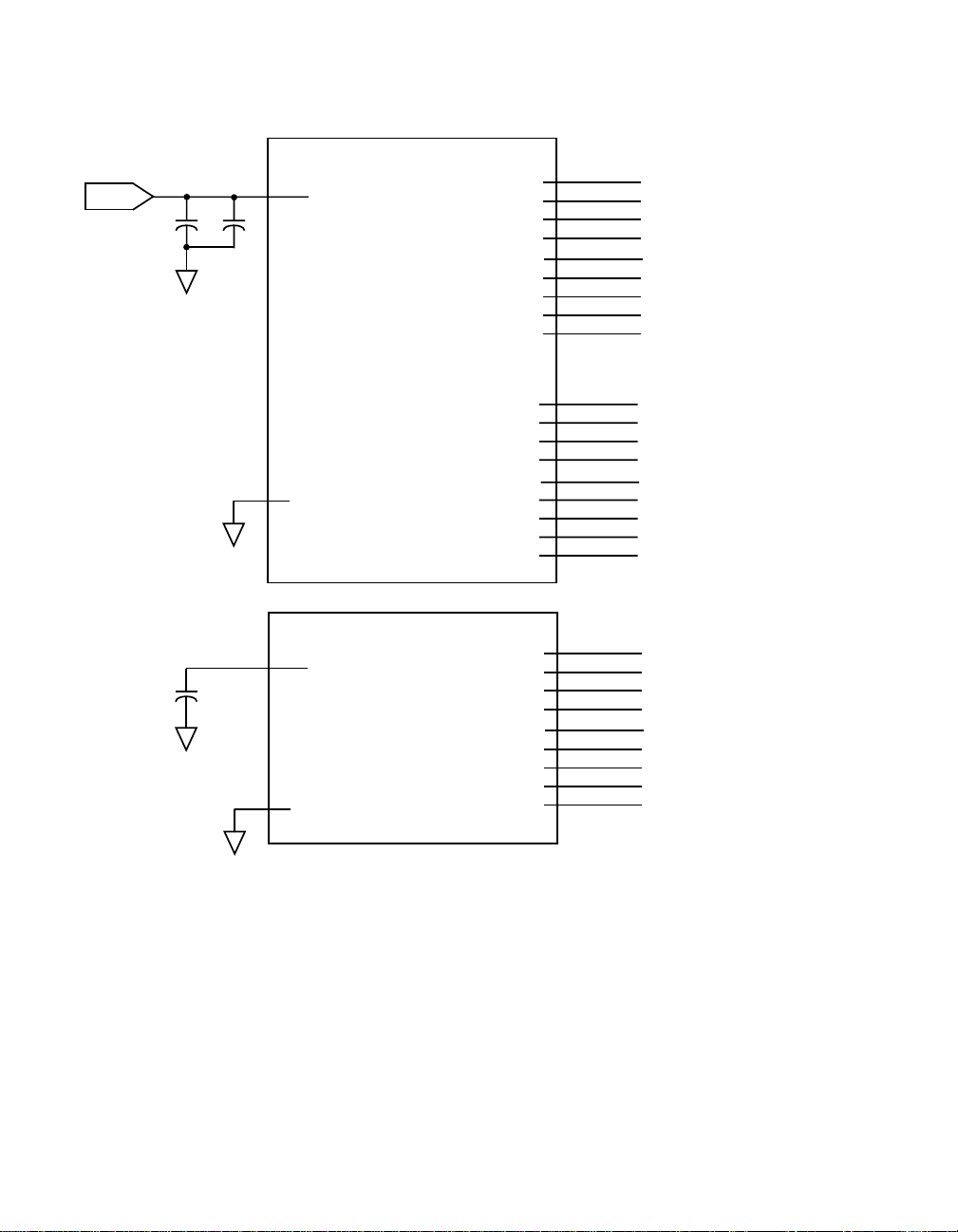
Figure 2.4 Regulated Termination
2.85 V
C1 C2
C3
2
REG_OUT
19
DISCONNECT
14
REG_OUT
6
DISCONNECT
UC5601QP
UC5603DP
TERML1
TERML2
TERML3
TERML4
TERML5
TERML6
TERML7
TERML8
TERML9
TERML10
TERML11
TERML12
TERML13
TERML14
TERML15
TERML16
TERML17
TERML18
TERML1
TERML2
TERML3
TERML4
TERML5
TERML6
TERML7
TERML8
TERML9
20
21
22
23
24
25
26
27
28
3
4
5
6
7
8
9
10
11
10
9
8
7
3
2
1
16
15
SD0 (J1.40)
SD1 (J1.41)
SD2 (J1.42)
SD3 (J1.43)
SD4 (J1.44)
SD5 (J1.45)
SD6 (J1.46)
SD7 (J1.47)
SDP (J1.48)
ATN (J1.55)
BSY (J1.57)
ACK (J1.58)
RST (J1.59)
MSG (J1.60)
SEL (J1.61)
C/D (J1.62)
REQ (J1.63)
I/O (J1.64)
SD15 (J1.38)
SD14 (J1.37)
SD13 (J1.36)
SD12 (J1.35)
SD11 (J1.68)
SD10 (J1.67)
SD9 (J1.66)
SD8 (J1.65)
SDP1 (J1.39)
Notes:
• C1 - 10 µF SMT
• C2 - 0.1 µF SMT
• C3 - 2.2 µF SMT
• J1 - 68-pin, high density “P” connector
2-24 Functional Description
Page 49

2.5.10 Select/Reselect During Selection/Reselection
In multithreaded SCSI I/O environments, it is not uncommon to be
selected or reselected while trying to perform selection/reselection. This
situation may occur when a SCSI controller (operating in the initiator
mode) tries to select a target and is reselected by another. The Select
SCRIPTS instruction has an alternate address to which the SCRIPTS will
jump when this situation occurs. The analogous situation for target
devices is being selected while trying to perform a reselection.
Once a change in operating mode occurs, the initiator SCRIPTS should
start with a Set Initiator instruction or the target SCRIPTS should start
with a Set Target instruction. The Selection and Reselection Enable bits
(SCSI Chip ID (SCID) bits 5 and 6, respectively) should both be asserted
so that the LSI53C875 may respond as an initiator or as a target. If only
selection is enabled, the LSI53C875 cannot be reselected as an initiator.
There are also status and interrupt bits in the SCSI Interrupt Status Zero
(SIST0) and SCSI Interrupt Enable Zero (SIEN0) registers, respectively,
indicating that the LSI53C875 has been selected (bit 5) and reselected
(bit 4).
2.5.11 Synchronous Operation
The LSI53C875 can transfer synchronous SCSI data in both the initiator
and target modes. The SCSI Transfer (SXFER) register controls both the
synchronous offset and the transfer period. It may be loaded by the CPU
before SCRIPTS execution begins, from within SCRIPTS using a Table
Indirect I/O instruction, or with a Read-Modify-Write instruction.
The LSI53C875 can receive data from the SCSI bus at a synchronous
transfer period as short as 50 ns, regardless of the transfer period used
to send data. The LSI53C875 can receive data at one-fourth of the
divided SCLK frequency. Depending on the SCLK frequency, the
negotiated transfer period, and the synchronous clock divider, the
LSI53C875 can send synchronous data at intervals as short as 50 ns for
Ultra SCSI, 100 ns for fast SCSI, and 200 ns for SCSI-1.
PCI Cache Mode 2-25
Page 50
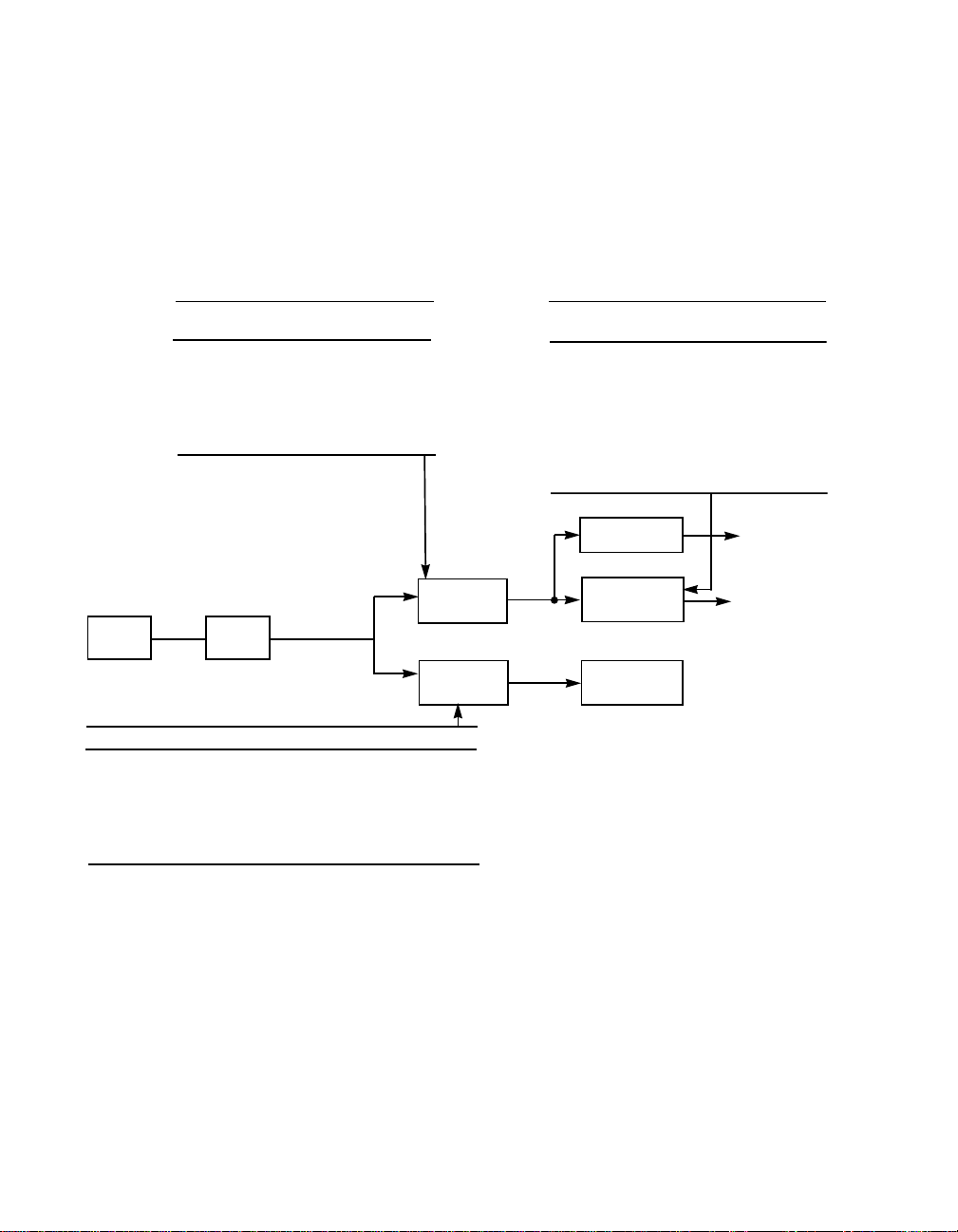
2.5.11.1 Determining the Data Transfer Rate
Synchronous data transfer rates are controlled by bits in two different
registers of the LSI53C875. Following is a brief description of the bits.
Figure 2.5 illustrates the clock division factors used in each register, and
the role of the register bits in determining the transfer rate.
Figure 2.5 Determining the Synchronous Transfer Rate
SCF2 SCF1 SCF0 SCF
0011
0 1 0 1.5
0112
1003
0003
1014
SCLK
CCF2 CCF1 CCF0 Divisor
0011
0 1 0 1.5
0112
1003
0003
1014
Clock
Doubler
Divisor
SCF
Divider
CCF
Divider
TP2 TP1 TP0 XFERP
Divisor
0004
0015
0106
0117
1008
1019
11010
11111
This point
must not
exceed
80 MHz
This point
must not
exceed
25 MHz
Example (8-bit SCSI bus):
SCLK = 80 MHz, SCF = 1 (÷ 1), XFERP = 4 (÷ 4),
CCF = 5 (÷ 4)
SCSI send rate = (SCLK ÷ SCF) ÷ XFERP
= (80 ÷ 1) ÷ 4 = 20 Mbytes/s
SCSI receive rate = (SCLK ÷ SCF) ÷ 4
= (80 ÷ 1) ÷ 4 = 20 Mbytes/s
Divide by 4
Synchronous
Divider
Asynchronous
SCSI Logic
Receive
Clock
Send Clock
(to SCSI Bus)
2.5.11.2 SCSI Control Three (SCNTL3) Register, Bits [6:4] (SCF[2:0])
The SCF[2:0] bits select the factor by which the frequency of SCLK is
divided before being presented to the synchronous SCSI control logic.
The output from this divider controls the rate at which data can be
received; this rate must not exceed 80 MHz. The receive rate of
synchronous SCSI data is one-fourth of the SCF divider output. For
2-26 Functional Description
Page 51

example, if SCLK is 80 MHz and the SCF value is set to divide by two,
then the maximum rate at which data can be received is 10 MHz
(80/(2*4) = 10).
2.5.11.3 SCSI Control Three (SCNTL3) Register, Bits [2:0] (CCF[2:0])
The CCF[2:0] bits select the factor by which the frequency of SCLK is
divided before being presented to the asynchronous SCSI core logic.
This divider must be set according to the input clock frequency in the
table.
2.5.11.4 SCSI Transfer (SXFER) Register, Bits [7:5] (TP[2:0])
The TP[2:0] divider bits determine the SCSI synchronous transfer period
when sending synchronous SCSI data in either initiator or target mode.
This value further divides the output from the SCF divider.
2.5.11.5 Achieving Optimal SCSI Send Rates
To achieve optimal synchronous SCSI send timings, the SCF divisor
value should be set high, to divide the clock as much as possible before
presenting the clock to the TP divider bits in the SCSI Transfer (SXFER)
register. The TP[2:0] divider value should be as low as possible. For
example, with an 80 MHz clock to achieve a 20 Mbytes/s Ultra SCSI
send rate, the SCF bits can be set to divide by 1 (001) and the TP bits
to divide by 4 (000). To set for a 10 Mbytes/s send rate for Fast SCSI2, the SCF bits can be set to divide by 2 (011) and the TP bits set to
divide by 4 (000).
2.5.12 Ultra SCSI Synchronous Data Transfers
Ultra SCSI is an extension of current Fast SCSI-2 synchronous transfer
specifications. It allows synchronous transfer periods to be negotiated
down as low as 50 ns, which is half the 100 ns period allowed under Fast
SCSI-2. This will allow a maximum transfer rate of 40 Mbytes/s on a
16-bit SCSI bus. The LSI53C875 requires an 80 MHz SCSI clock input
to perform Ultra SCSI transfers. In addition, the following bit values affect
the chip’s ability to support Ultra SCSI synchronous transfer rates:
• Clock Conversion Factor bits, SCSI Control Three (SCNTL3) register
bits [2:0] and Synchronous Clock Conversion Factor bits, SCSI
Control Three (SCNTL3) register bits [6:4]. These fields now support
PCI Cache Mode 2-27
Page 52

a value of 101 (binary), allowing the SCLK frequency to be divided
down by 4. This allows systems using an 80 MHz clock or the
internal clock doubler to operate at Fast SCSI-2 transfer rates as well
as Ultra SCSI rates, if needed.
• Ultra Mode Enable bit, SCSI Control Three (SCNTL3) register bit 7.
Setting this bit enables Ultra SCSI synchronous transfers in systems
that have an 80 MHz clock or use the internal SCSI clock doubler.
2.5.13 Interrupt Handling
The SCRIPTS processors in the LSI53C875 perform most functions
independently of the host microprocessor. However, certain interrupt
situations must be handled by the external microprocessor. This section
explains all aspects of interrupts as they apply to the LSI53C875.
2.5.13.1 Polling and Hardware Interrupts
The external microprocessor is informed of an interrupt condition by
polling or hardware interrupts. Polling means that the microprocessor
must continually loop and read a register until it detects a bit set that
indicates an interrupt. This method is the fastest, but it wastes CPU time
that could be used for other system tasks. The preferred method of
detecting interrupts in most systems is hardware interrupts. In this case,
the LSI53C875 asserts the Interrupt Request (IRQ/) line that interrupts
the microprocessor, causing the microprocessor to execute an interrupt
service routine. A hybrid approach would use hardware interrupts for
long waits, and use polling for short waits.
2.5.13.2 Registers
The registers in the LSI53C875 that are used for detecting or defining
interrupts are the Interrupt Status (ISTAT), SCSI Interrupt Status Zero
(SIST0), SCSI Interrupt Status One (SIST1), DMA Status (DSTAT), SCSI
Interrupt Enable Zero (SIEN0), SCSI Interrupt Enable One (SIEN1), DMA
Control (DCNTL), and DMA Interrupt Enable (DIEN).
ISTAT – The ISTAT register is the only register that can be accessed as
a slave during SCRIPTS operation. Therefore it is the register that is
polled when polled interrupts are used. It is also the first register that
should be read when the IRQ/ pin has been asserted in association with
2-28 Functional Description
Page 53

a hardware interrupt. The INTF (Interrupt-on-the-Fly) bit should be the
first interrupt serviced. It must be written to one to be cleared. This
interrupt must be cleared before servicing any other interrupts.
If the SIP bit in the Interrupt Status (ISTAT) register is set, then a
SCSI-type interrupt has occurred and the SCSI Interrupt Status Zero
(SIST0) and SCSI Interrupt Status One (SIST1) registers should be read.
If the DIP bit in the Interrupt Status (ISTAT) register is set, then a
DMA-type interrupt has occurred and the DMA Status (DSTAT) register
should be read.
SCSI-type and DMA-type interrupts may occur simultaneously, so in
some cases both SIP and DIP may be set.
SIST0 and SIST1 – The SCSI Interrupt Status Zero (SIST0) and SCSI
Interrupt Status One (SIST1) registers contain the SCSI-type interrupt
bits. Reading these registers determines which condition or conditions
caused the SCSI-type interrupt, and clears that SCSI interrupt condition.
If the LSI53C875 is receiving data from the SCSI bus and a fatal interrupt
condition occurs, the chip attempts to send the contents of the DMA
FIFO to memory before generating the interrupt.
If the LSI53C875 is sending data to the SCSI bus and a fatal SCSI
interrupt condition occurs, data could be left in the DMA FIFO. Because
of this, the DMA FIFO Empty (DFE) bit in DMA Status (DSTAT) should
be checked.
If this bit is cleared, set the CLF (Clear DMA FIFO) and CSF (Clear SCSI
FIFO) bits before continuing. The CLF bit is bit 2 in Chip Test Three
(CTEST3). The CSF bit is bit 1 in SCSI Test Three (STEST3).
DSTAT – The DMA Status (DSTAT) register contains the DMA-type
interrupt bits. Reading this register determines which condition or
conditions caused the DMA-type interrupt, and clears that DMA interrupt
condition. Bit 7 in DSTAT, DFE, is purely a status bit; it will not generate
an interrupt under any circumstances and will not be cleared when read.
DMA interrupts flush neither the DMA nor SCSI FIFOs before generating
the interrupt, so the DFE bit in the DMA Status (DSTAT) register should
be checked after any DMA interrupt.
PCI Cache Mode 2-29
Page 54

If the DFE bit is cleared, then the FIFOs must be cleared by setting the
CLF (Clear DMA FIFO) and CSF (Clear SCSI FIFO) bits, or flushed by
setting the FLF (Flush DMA FIFO) bit.
SIEN0 and SIEN1 – The SCSI Interrupt Enable Zero (SIEN0) and SCSI
Interrupt Enable One (SIEN1) registers are the interrupt enable registers
for the SCSI interrupts in SCSI Interrupt Status Zero (SIST0) and SCSI
Interrupt Status One (SIST1).
DIEN – The DMA Interrupt Enable (DIEN) register is the interrupt enable
register for DMA interrupts in DMA Status (DSTAT).
DCNTL – When bit 1 in this register is set, the IRQ/ pin is not asserted
when an interrupt condition occurs. The interrupt is not lost or ignored,
but merely masked at the pin. Clearing this bit when an interrupt is
pending immediately causes the IRQ/ pin to assert. As with any register
other than ISTAT, this register cannot be accessed except by a
SCRIPTS instruction during SCRIPTS execution.
2.5.13.3 Fatal vs. Nonfatal Interrupts
A fatal interrupt, as the name implies, always causes SCRIPTS to stop
running. All nonfatal interrupts become fatal when they are enabled by
setting the appropriate interrupt enable bit. Interrupt masking is
discussed Section 2.5.13.4, “Masking.” All DMA interrupts (indicated by
the DIP bit in ISTAT and one or more bits in DMA Status (DSTAT) being
set) are fatal.
Some SCSI interrupts (indicated by the SIP bit in the ISTAT and one or
more bits in SCSI Interrupt Status Zero (SIST0) or SCSI Interrupt Status
One (SIST1) being set) are nonfatal.
When the LSI53C875 is operating in Initiator mode, only the Function
Complete (CMP), Selected (SEL), Reselected (RSL), General Purpose
Timer Expired (GEN), and Handshake-to-Handshake Timer Expired
(HTH) interrupts are nonfatal.
When operating in Target mode CMP, SEL, RSL, Target mode: SATN/
active (M/A), GEN, and HTH are nonfatal. Refer to the description for the
Disable Halt on a Parity Error or SATN/ active (Target Mode Only) (DHP)
bit in the SCSI Control One (SCNTL1) register to configure the chip’s
2-30 Functional Description
Page 55

2.5.13.4 Masking
behavior when the SATN/ interrupt is enabled during Target mode
operation. The Interrupt-on-the-Fly interrupt is also nonfatal, since
SCRIPTS can continue when it occurs.
The reason for nonfatal interrupts is to prevent SCRIPTS from stopping
when an interrupt occurs that does not require service from the CPU.
This prevents an interrupt when arbitration is complete (CMP set), when
the LSI53C875 has been selected or reselected (SEL or RSL set), when
the initiator asserts ATN (target mode: SATN/ active), or when the
General Purpose or Handshake-to-Handshake timers expire. These
interrupts are not needed for events that occur during high-level
SCRIPTS operation.
Masking an interrupt means disabling or ignoring that interrupt. Interrupts
can be masked by clearing bits in the SCSI Interrupt Enable Zero
(SIEN0) and SCSI Interrupt Enable One (SIEN1) (for SCSI interrupts)
registers or DMA Interrupt Enable (DIEN) (for DMA interrupts) register.
How the chip responds to masked interrupts depends on: whether polling
or hardware interrupts are being used; whether the interrupt is fatal or
nonfatal; and whether the chip is operating in Initiator or Target mode.
If a nonfatal interrupt is masked and that condition occurs, the SCRIPTS
do not stop, the appropriate bit in the SCSI Interrupt Status Zero (SIST0)
or SCSI Interrupt Status One (SIST1) is still set, the SIP bit in the
Interrupt Status (ISTAT) is not set, and the IRQ/ pin is not asserted. See
Section 2.5.13.3, “Fatal vs. Nonfatal Interrupts,” for a list of the nonfatal
interrupts.
If a fatal interrupt is masked and that condition occurs, then the
SCRIPTS still stop, the appropriate bit in the DMA Status (DSTAT), SCSI
Interrupt Status Zero (SIST0),orSCSI Interrupt Status One (SIST1)
register is set, and the SIP or DIP bits in the Interrupt Status (ISTAT) is
set, but the IRQ/ pin is not asserted.
When the chip is initialized, enable all fatal interrupts if you are using
hardware interrupts. If a fatal interrupt is disabled and that interrupt
condition occurs, SCRIPTS halts and the system will never know it
unless it times out and checks the ISTAT after a certain period of
inactivity.
PCI Cache Mode 2-31
Page 56

If you are polling the ISTAT instead of using hardware interrupts, then
masking a fatal interrupt makes no difference since the SIP and DIP bits
in the Interrupt Status (ISTAT) inform the system of interrupts, not the
IRQ/ pin.
Masking an interrupt after IRQ/ is asserted does not cause IRQ/ to be
deasserted.
2.5.13.5 Stacked Interrupts
The LSI53C875 will stack interrupts if they occur one after the other. If
the SIP or DIP bits in the ISTAT register are set (first level), then there
is already at least one pending interrupt, and any future interrupts are
stacked in extra registers behind the SCSI Interrupt Status Zero (SIST0),
SCSI Interrupt Status One (SIST1), and DMA Status (DSTAT) registers
(second level). When two interrupts have occurred and the two levels of
the stack are full, any further interrupts set additional bits in the extra
registers behind SCSI Interrupt Status Zero (SIST0), SCSI Interrupt
Status One (SIST1), and DMA Status (DSTAT). When the first level of
interrupts are cleared, all the interrupts that came in afterward move into
the SIST0, SIST1, and DSTAT. After the first interrupt is cleared by
reading the appropriate register, the IRQ/ pin is deasserted for a
minimum of three CLKs; the stacked interrupts move into the SCSI
Interrupt Status Zero (SIST0), SCSI Interrupt Status One (SIST1),or
DMA Status (DSTAT); and the IRQ/ pin is asserted once again.
Since a masked nonfatal interrupt does not set the SIP or DIP bits,
interrupt stacking does not occur. A masked, nonfatal interrupt still posts
the interrupt in SIST0, but does not assert the IRQ/ pin. Since no
interrupt is generated, future interrupts move right into the SCSI Interrupt
Status Zero (SIST0) or SCSI Interrupt Status One (SIST1) instead of
being stacked behind another interrupt. When another condition occurs
that generates an interrupt, the bit corresponding to the earlier masked
nonfatal interrupt is still set.
A related situation to interrupt stacking is when two interrupts occur
simultaneously. Since stacking does not occur until the SIP or DIP bits
are set, there is a small timing window in which multiple interrupts can
occur but will not be stacked. These could be multiple SCSI interrupts
(SIP set), multiple DMA interrupts (DIP set), or multiple SCSI and
multiple DMA interrupts (both SIP and DIP set).
2-32 Functional Description
Page 57

As previously mentioned, DMA interrupts do not attempt to flush the
FIFOs before generating the interrupt. It is important to set either the
Clear DMA FIFO (CLF) and Clear SCSI FIFO (CSF) bits if a DMA
interrupt occurs and the DMA FIFO Empty (DFE) bit is not set. This is
because any future SCSI interrupts are not posted until the DMA FIFO
is cleared of data. These ‘locked out’ SCSI interrupts are posted as soon
as the DMA FIFO is empty.
2.5.13.6 Halting in an Orderly Fashion
When an interrupt occurs, the LSI53C875 attempts to halt in an orderly
fashion.
• If the interrupt occurs in the middle of an instruction fetch, the fetch
is completed, except in the case of a Bus Fault. Execution does not
begin, but the DMA SCRIPTS Pointer (DSP) points to the next
instruction since it is updated when the current instruction is fetched.
• If the DMA direction is a write to memory and a SCSI interrupt
occurs, the LSI53C875 attempts to flush the DMA FIFO to memory
before halting. Under any other circumstances only the current cycle
is completed before halting, so the DFE bit in DSTAT should be
checked to see if any data remains in the DMA FIFO.
• SCSI SREQ/SACK handshakes that have begun are completed
before halting.
• The LSI53C875 attempts to clean up any outstanding synchronous
offset before halting.
• In the case of Transfer Control Instructions, once instruction
execution begins it continues to completion before halting.
• If the instruction is a JUMP/CALL WHEN/IF <phase>, the DMA
SCRIPTS Pointer (DSP) is updated to the transfer address before
halting.
• All other instructions may halt before completion.
2.5.13.7 Sample Interrupt Service Routine
The following is a sample of an interrupt service routine for the
LSI53C875. It can be repeated during polling or should be called when
the IRQ/ pin is asserted during hardware interrupts.
PCI Cache Mode 2-33
Page 58

1. Read Interrupt Status (ISTAT).
2. If the INTF bit is set, it must be written to a one to clear this status.
3. If only the SIP bit is set, read SCSI Interrupt Status Zero (SIST0) and
SCSI Interrupt Status One (SIST1) to clear the SCSI interrupt
condition and get the SCSI interrupt status. The bits in the SIST0
and SIST1 tell which SCSI interrupts occurred and determine what
action is required to service the interrupts.
4. If only the DIP bit is set, read the DMA Status (DSTAT) to clear the
interrupt condition and get the DMA interrupt status. The bits in
DSTAT tell which DMA interrupts occurred and determine what
action is required to service the interrupts.
5. If both the SIP and DIP bits are set, read SCSI Interrupt Status Zero
(SIST0), SCSI Interrupt Status One (SIST1), and DMA Status
(DSTAT) to clear the SCSI and DMA interrupt condition and get the
interrupt status. If using 8-bit reads of the SIST0, SIST1, and DSTAT
registers to clear interrupts, insert a 12 CLK delay between the
consecutive reads to ensure that the interrupts clear properly. Both
the SCSI and DMA interrupt conditions should be handled before
leaving the interrupt service routine. It is recommended that the DMA
interrupt be serviced before the SCSI interrupt, because a serious
DMA interrupt condition could influence how the SCSI interrupt is
acted upon.
6. When using polled interrupts, go back to Step 1 before leaving the
interrupt service routine, in case any stacked interrupts moved in
when the first interrupt was cleared. When using hardware interrupts,
the IRQ/ pin is asserted again if there are any stacked interrupts.
This should cause the system to re-enter the interrupt service
routine.
2.5.14 Chained Block Moves
Since the LSI53C875 has the capability to transfer 16-bit wide SCSI
data, a unique situation occurs when dealing with odd bytes. The
Chained Move (CHMOV) SCRIPTS instruction along with the Wide SCSI
Send (WSS) and Wide SCSI Receive (WSR) bits in the SCSI Control
Two (SCNTL2) register are used to facilitate these situations. The
Chained Block Move instruction is illustrated in Figure 2.6.
2-34 Functional Description
Page 59
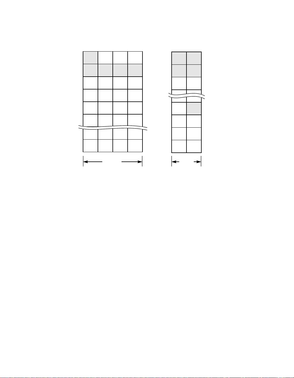
Figure 2.6 Block Move and Chained Block Move Instructions
Host Memory SCSI Bus
0x03 0x02 0x01 0x00
0x07 0x06 0x05 0x04
0x0B 0x0A 0x09 0x08
0x0F 0x0E 0x0D 0x0C
0x13 0x12 0x11 0x10
32 Bits 16 Bits
00
04
08
0C
10
0x04 0x03
0x06 0x05
0x09 0x07
0x0B 0x0A
0x0D 0x0C
CHMOV 5, 3 when Data_Out
Moves five bytes from address 0x03 in the host memory to the SCSI bus.
Bytes 0x03, 0x04, 0x05, and 0x06 are moved and byte 0x07 remains in
the low-order byte of the SCSI Output Data Latch (SODL) register and
is combined with the first byte of the following MOVE instruction.
Move 5, 9 when Data_Out
Moves five bytes from address 0x09 in the host memory to the SCSI bus.
2.5.14.1 Wide SCSI Send Bit
The WSS bit is set whenever the SCSI controller is sending data
(Data-Out for initiator or Data-In for target) and the controller detects a
partial transfer at the end of a chained Block Move SCRIPTS instruction
(this flag is not set if a normal Block Move instruction is used). Under this
condition, the SCSI controller does not send the low-order byte of the last
partial memory transfer across the SCSI bus. Instead, the low-order byte
is temporarily stored in the lower byte of the SCSI Output Data Latch
(SODL) register and the WSS flag is set. The hardware uses the WSS
flag to determine what behavior must occur at the start of the next data
PCI Cache Mode 2-35
Page 60

send transfer. When the WSS flag is set at the start of the next transfer,
the first byte (the high-order byte) of the next data send transfer is
“married” with the stored low-order byte in the SODL register; and the
two bytes are sent out across the bus, regardless of the type of Block
Move instruction (normal or chained). The flag is automatically cleared
when the “married” word is sent. The flag can alternately be cleared
through SCRIPTS or by the microprocessor. Also, the microprocessor or
SCRIPTS can use this bit for error detection and recovery purposes.
2.5.14.2 Wide SCSI Receive Bit
The WSR bit is set whenever the SCSI controller is receiving data
(Data-In for initiator or Data-Out for target) and the controller detects a
partial transfer at the end of a block move or chained block move
SCRIPTS instruction. When WSR is set, the high-order byte of the last
SCSI bus transfer is not transferred to memory. Instead, the byte is
temporarily stored in the SCSI Wide Residue (SWIDE) register. The
hardware uses the WSR bit to determine what behavior must occur at
the start of the next data receive transfer. The bit is automatically cleared
at the start of the next data receive transfer. The bit can alternatively be
cleared by the microprocessor or through SCRIPTS. The bit can also be
used by the microprocessor or SCRIPTS for error detection and recovery
purposes.
2.5.14.3 SWIDE Register
This register stores data for partial byte data transfers. For receive data,
the SCSI Wide Residue (SWIDE) register holds the high-order byte of a
partial SCSI transfer which has not yet been transferred to memory. This
stored data may be a residue byte (and therefore ignored) or it may be
valid data that is transferred to memory at the beginning of the next Block
Move instruction.
2.5.14.4 SODL Register
For send data, the low-order byte of the SCSI Output Data Latch (SODL)
register holds the low-order byte of a partial memory transfer which has
not yet been transferred across the SCSI bus. This stored data is usually
“married” with the first byte of the next data send transfer, and both bytes
are sent across the SCSI bus at the start of the next data send block
move command.
2-36 Functional Description
Page 61

2.5.14.5 Chained Block Move SCRIPTS Instruction
A chained Block Move SCRIPTS instruction is primarily used to transfer
consecutive data send or data receive blocks. Using the chained Block
Move instruction facilitates partial receive transfers and allows correct
partial send behavior without additional opcode overhead. Behavior of
the chained Block Move instruction varies slightly for sending and
receiving data.
For receive data (Data-In for initiator or Data-Out for target), a chained
Block Move instruction indicates that if a partial transfer occurred at the
end of the instruction, the WSR flag is set. The high-order byte of the
last SCSI transfer is stored in the SCSI Wide Residue (SWIDE) register
rather than transferred to memory. The contents of the SWIDE register
should be the first byte transferred to memory at the start of the chained
Block Move data stream. Since the byte count always represents data
transfers to/from memory (as opposed to the SCSI bus), the byte
transferred out of the SCSI Wide Residue (SWIDE) register is one of the
bytes in the byte count. If the WSR bit is clear when a receive data
chained Block Move instruction is executed, the data transfer occurs
similar to that of the regular Block Move instruction. Whether the WSR
bit is set or clear, when a normal block move instruction is executed, the
contents of the SCSI Wide Residue (SWIDE) register are ignored and
the transfer takes place normally. For “N” consecutive wide data receive
Block Move instructions, the 2nd through the Nth Block Move instructions
should be Chained Block Moves.
For send data (Data-Out for initiator or Data-In for target), a chained
Block Move instruction indicates that if a partial transfer terminates the
chained Block Move instruction, the last low-order byte (the partial
memory transfer) should be stored in the lower byte of the SCSI Output
Data Latch (SODL) register and not sent across the SCSI bus. Without
the chained block move instruction, the last low-order byte would be sent
across the SCSI bus. The starting byte count represents data bytes
transferred from memory but not to the SCSI bus when a partial transfer
exists. For example, if the instruction is an Initiator chained Block Move
Data Out of five bytes (and WSS is not previously set), five bytes are
transferred out of memory to the SCSI controller, four bytes are
transferred from the SCSI controller across the SCSI bus, and one byte
is temporarily stored in the lower byte of the SCSI Output Data Latch
(SODL) register waiting to be married with the first byte of the next Block
Move instruction. Regardless of whether a chained Block Move or normal
PCI Cache Mode 2-37
Page 62

Block Move instruction is used, if the WSS bit is set at the start of a data
send command, the first byte of the data send command is assumed to
be the high-order byte and is “married” with the low-order byte stored in
the lower byte of the SCSI Output Data Latch (SODL) register before the
two bytes are sent across the SCSI bus. For “N” consecutive wide data
send Block Move commands, the first through the (Nth – 1) Block Move
instructions should be Chained Block Moves.
2.6 Power Management
The LSI53C875E complies with the PCI Bus Power Management
Interface Specification, Revision 1.0. The PCI Function Power States D0,
D1, D2, and D3 are defined in that specification. D0 and D3 are required
by specification, and D1 and D2 are optional. D0 is the maximum
powered state, and D3 is the minimum powered state. Power state D3
is further categorized as D3hot or D3cold. A function that is powered off
is said to be in the D3cold power state.
The power states for the SCSI function are independently controlled
through two power state bits that are located in the PCI Configuration
Space register 0x44. The bits are encoded as:
00b D0
01b Reserved
10b Reserved
11b D3
Power states D1 and D2 are not discussed because they have not been
implemented as a new feature.
The Power states – D0 and D3 – are described below in conjunction with
each SCSI function. Power state actions are separate for each function.
2.6.1 Power State D0
Power state D0 is the maximum power state and is the power-up default
state for each function.
2-38 Functional Description
Page 63

2.6.2 Power State D3
Power state D3 is the minimum power state, which includes subsettings
called D3hot and D3cold. The devices are considered to be in power
state D3cold when power is removed from them. D3cold can transition
to D0 by applying VCCand resetting the device. D3hot allows the device
to transition to D0 using software. To obtain power reduction in D3hot,
the SCSI clock and the SCSI clock doubler Phase Lock Loop (PLL) are
disabled. Furthermore, the function’s soft reset is continually asserted
while in power state D3, which clears all pending interrupts and 3-states
the SCSI bus. In addition, the function’s PCI Command register is
cleared.
Power Management 2-39
Page 64

2-40 Functional Description
Page 65

Chapter 3
PCI Functional
Description
This chapter is divided into the following sections:
• Section 3.1, “PCI Addressing”
• Section 3.2, “PCI Cache Mode”
• Section 3.3, “Configuration Registers”
3.1 PCI Addressing
There are three types of PCI-defined address space:
• Configuration space
• Memory space
• I/O space
The configuration space is a contiguous 256 x 8-bit set of addresses
dedicated to each “slot” or “stub” on the bus. Decoding C_BE/[3:0]
determines if a PCI cycle is intended to access configuration register
space. The IDSEL bus signal is a “chip select” that allows access to the
configuration register space only. A configuration read/write cycle without
IDSEL is ignored. The eight lower order addresses select a specific 8-bit
register. AD[10:8] are decoded as well, but they must be zero or the
LSI53C875 does not respond. According to the PCI specification,
AD[10:8] are reserved for multifunction devices. The host processor uses
the PCI configuration space to initialize the LSI53C875.
The lower 128 bytes of the LSI53C875 configuration space holds system
parameters while the upper 128 bytes map into the LSI53C875 operating
registers. For all PCI cycles except configuration cycles, the LSI53C875
registers are located on the 256-byte blockboundary defined by the base
LSI53C875/875E PCI to Ultra SCSI I/O Processor 3-1
Page 66

address assigned through the configured register. The LSI53C875
operating registers are available in both the upper and lower 128-byte
portions of the 256-byte space selected.
At initialization time, each PCI device is assigned a base address (in the
case of the LSI53C875, the upper 24 bits of the address are selected)
for memory and I/O accesses. On every access, the LSI53C875
compares its assigned base addresses with the value on the
Address/Data bus during the PCI address phase. If the upper 24 bits
match, the access is for the LSI53C875 and the low-order eight bits
define the register to be accessed. A decode of C_BE/[3:0] determines
which registers and what type of access is to be performed.
The PCI specification defines memory space as a contiguous 32-bit
memory address that is shared by all system resources, including the
LSI53C875. Base Address One (Memory) determines which 256-byte
memory area this device occupies.
The PCI specification defines I/O space as a contiguous 32-bit I/O
address that is shared by all system resources, including the LSI53C875.
Base Address Zero (I/O) determines which 256-byte I/O area this device
occupies.
3.1.1 PCI Bus Commands and Functions Supported
Bus commands indicate to the target the type of transaction the master
is requesting. Bus commands are encoded on the C_BE/[3:0] lines
during the address phase. PCI bus command encoding and types appear
in Table 3.1.
3-2 PCI Functional Description
Page 67

Table 3.1 PCI Bus Commands and Encoding Types
C_BE[3:0] Command Type Supported as Master Supported as Slave
0000 Special Interrupt Acknowledge No No
0001 Special Cycle No No
0010 I/O Read Cycle Yes Yes
0011 I/O Write Cycle Yes Yes
0100 Reserved N/A N/A
0101 Reserved N/A N/A
0110 Memory Read Yes Yes
0111 Memory Write Yes Yes
1000 Reserved N/A N/A
1001 Reserved N/A N/A
1010 Configuration Read No Yes
1011 Configuration Write No Yes
1100 Memory Read Multiple Yes
1
No (defaults to 0110)
1101 Dual Address Cycle No No
1110 Memory Read Line Yes
1111 Memory Write and Invalidate Yes
1. This operation is selectable by bit 2 in the DMA Mode (DMODE) operating register.
2. This operation is selectable by bit 3 in the DMA Mode (DMODE) operating register.
3. This operation is selectable by bit 0 in the Chip Test Three (CTEST3) operating register.
2
3
No (defaults to 0110)
No (defaults to 0111)
3.1.1.1 I/O Read Command
The I/O Read command reads data from an agent mapped in I/O
address space. All 32 address bits are decoded.
3.1.1.2 I/O Write Command
The I/O Write command writes data to an agent when mapped in I/O
address space. All 32 address bits are decoded.
PCI Addressing 3-3
Page 68

3.1.1.3 Memory Read
The Memory Read command reads data from an agent mapped in
memory address space. All 32 address bits are decoded.
3.1.1.4 Memory Read Multiple
The Memory Read command reads data from an agent mapped in
memory address space. All 32 address bits are decoded.
3.1.1.5 Memory Read Line
The Memory Read command reads data from an agent mapped in
memory address space. All 32 address bits are decoded.
3.1.1.6 Memory Write
The Memory Write command writes data to an agent when mapped in
memory address space. All 32 address bits are decoded.
3.1.1.7 Memory Write and Invalidate
The Memory Write command writes data to an agent when mapped in
memory address space. All 32 address bits are decoded.
3.2 PCI Cache Mode
The LSI53C875 supports the PCI specification for an 8-bit Cache Line
Size register located in the PCI configuration space. The Cache Line
Size register provides the ability to sense and react to nonaligned
addresses corresponding to cache line boundaries. In conjunction with
the Cache Line Size register, the PCI commands Read Line, Read
Multiple, and Write and Invalidate are each software enabled or disabled
to allow the user full flexibility in using these commands.
3.2.1 Support for PCI Cache Line Size Register
The LSI53C875 supports the PCI specification for an 8-bit Cache Line
Size register in PCI configuration space. It can sense and react to
nonaligned addresses corresponding to cache line boundaries.
3-4 PCI Functional Description
Page 69

3.2.2 Selection of Cache Line Size
The cache logic selects a cache line size based on the values for the
burst size in the DMA Mode (DMODE) register, bit 2 in the Chip Test Five
(CTEST5) register, and the PCI Cache Line Size register.
Note: The LSI53C875 does not automatically use the value in the
PCI Cache Line Size register as the cache line size value.
The chip scales the value of the Cache Line Size register
down to the nearest binary burst size allowed by the chip
(2, 4, 8, 16, 32, 64, or 128), compares this value to the
burst size defined by the values of the DMA Mode
(DMODE) register and bit 2 of the Chip TestFive (CTEST5)
register, then selects the smallest as the value for the
cache line size. The LSI53C875 uses this value for all burst
data transfers.
3.2.3 Alignment
The LSI53C875 uses the calculated line size value to monitor the current
address for alignment to the cache line size. When it is not aligned, the
chip attempts to align to the cache boundary by using a “smart aligning”
scheme. This means that it attempts to use the largest burst size
possible that is less than the cache line size, to reach the cache
boundary quickly with no overflow. This process is a stepping
mechanism that steps up to the highest possible burst size based on the
current address.
The stepping process begins ata4Dwordboundary. The LSI53C875 will
first try to align to a 4 Dword boundary (0x00, 0x010, 0x020, etc.) by
using single Dword transfers (no bursting). Once this boundary is
reached the chip evaluates the current alignment to various burst sizes
allowed, and selects the largest possible as the next burst size, while not
exceeding the cache line size. The chip then issues this burst, and
reevaluates the alignment to various burst sizes, again selecting the
largest possible while not exceeding the cache line size, as the next
burst size. This stepping process continues until the chip reaches the
cache line size boundary or runs out of data. Once a cache line boundary
is reached, the chip uses the cache line size as the burst size from then
on, except in the case of multiples (explained below). The alignment
process is finished at this point.
PCI Cache Mode 3-5
Page 70

Example: Cache Line Size - 16, Current Address = 0x01 – The chip
is not aligned to a 4 Dword cache boundary (the stepping threshold), so
it issues four single Dword transfers (the first is a 3-byte transfer). At
address 0x10, the chip is aligned to a 4 Dword boundary, but not aligned
to any higher burst size boundaries that are less than the cache line size.
So, the part issues a burst of 4. At this point, the address is 0x20, and
the chip evaluates that it is aligned not only toa4Dwordboundary, but
also to an 8 Dword boundary. It selects the highest, 8, and bursts
8 Dwords. At this point, the address is 0x40, which is a cache line size
boundary. Alignment stops, and the burst size from then on is switched
to 16.
3.2.4 Memory Move Misalignment
The LSI53C875 does not operate in a cache alignment mode when a
Memory Move instruction type is issued and the read and write
addresses are different distances from the nearest cache line boundary.
For example, if the read address is 0x21F and the write address is
0x42F, and the cache line size is 8, the addresses are byte aligned, but
they are not the same distance from the nearest cache boundary. The
read address is 1 byte from the cache boundary 0x220 and the write
address is 17 bytes from the cache boundary 0x440. In this situation, the
chip does not align to cache boundaries and operates as an LSI53C825.
3.2.5 Memory Write and Invalidate Command
The Memory Write and Invalidate command is identical to the Memory
Write command, except that it additionally guarantees a minimum
transfer of one complete cache line; that is to say, the master intends to
write all bytes within the addressed cache line in a single PCI transaction
unless interrupted by the target. This command requires implementation
of the PCI Cache Line Size register at address 0x0C in PCI configuration
space. The LSI53C875 enables Memory Write and Invalidate cycles
when bit 0 in the Chip Test Three (CTEST3) register (WRIE) and bit 4 in
the PCI Command register are set. When the following conditions are
met, Memory Write and Invalidate commands are issued:
1. The CLSE bit (Cache Line Size Enable, bit 7, DMA Control (DCNTL)
register), WRIE bit (Write and Invalidate Enable, bit 0, Chip Test
Three (CTEST3) register), and PCI configuration Command register,
bit 4 are set.
3-6 PCI Functional Description
Page 71

2. The Cache Line Size register contains a legal burst size (2, 4, 8, 16,
32, 64, or 128) value and that value must be less than or equal to
the DMA Mode (DMODE) burst size.
3. The chip has enough bytes in the DMA FIFO to complete at least
one full cache line burst.
4. The chip is aligned to a cache line boundary.
When these conditions are met, the LSI53C875 issues a Write and
Invalidate command instead of a Memory Write command during all PCI
write cycles.
Multiple Cache Line Transfers – The Write and Invalidate command
can write multiple cache lines of data in a single bus ownership. The chip
issues a burst transfer as soon as it reaches a cache line boundary. The
size of the transfer is not automatically the cache line size, but rather a
multiple of the cache line size specified in the Revision 2.1 of the PCI
specification. The logic selects the largest multiple of the cache line size
based on the amount of data to transfer, with the maximum allowable
burst size being that determined from the DMA Mode (DMODE) burst
size bits and Chip Test Five (CTEST5), bit 2. If multiple cache line size
transfers are not desired, set the DMA Mode (DMODE) burst size to
exactly the cache line size and the chip only issues single cache line
transfers.
3.2.5.1 Latency
After each data transfer, the chip re-evaluates the burst size based on
the amount of remaining data to transfer and again selects the highest
possible multiple of the cache line size, no larger than the DMA Mode
(DMODE) burst size. The most likely scenario of this scheme is that the
chip selects the DMA Mode (DMODE) burst size after alignment, and
issues bursts of this size. The burst size is, in effect, throttled down
toward the end of a long Memory Move or Block Move transfer until only
the cache line size burst size is left. The chip finishes the transfer with
this burst size.
In accordance with the PCI specification, the latency timer is ignored
when issuing a Write and Invalidate command such that when a latency
time-out occurs, the LSI53C875 continues to transfer up to a cache line
boundary. At that point, the chip relinquishes the bus, and finishes the
PCI Cache Mode 3-7
Page 72

transfer at a later time using another bus ownership. If the chip is
transferring multiple cache lines it continues to transfer until the next
cache boundary is reached.
PCI Target Retry – During a Write and Invalidate transfer, if the target
device issues a retry (STOP with no TRDY, indicating that no data was
transferred), the chip relinquishes the bus and immediately tries to finish
the transfer on another bus ownership. The chip issues another Write
and Invalidate command on the next ownership, in accordance with the
PCI specification.
PCI Target Disconnect – During a Write and Invalidate transfer, if the
target device issues a disconnect the LSI53C875 relinquishes the bus
and immediately tries to finish the transfer on another bus ownership.
The chip does not issue another Write and Invalidate command on the
next ownership unless the address is aligned.
3.2.6 Memory Read Line Command
This command is identical to the Memory Read command, except that it
additionally indicates that the master intends to fetch a complete cache
line. This command is intended for use with bulk sequential data
transfers where the memory system and the requesting master might
gain some performance advantage by reading up to a cache line
boundary rather than a single memory cycle. The Read Line function in
the LSI53C875 takes advantage of the PCI 2.1 specification regarding
issuing this command. The functionality of the Enable Read Line bit (bit
3inDMA Mode (DMODE)) has been modified to more resemble the
Write and Invalidate mode in terms of conditions that must be met before
a Read Line command is issued. However, the Read Line option
operates exactly like the previous LSI53C8XX chips when cache mode
has been disabled by a CLSE bit reset or when certain conditions exist
in the chip (explained below).
The Read Line mode is enabled by setting bit 3 in the DMA Mode
(DMODE) register. If cache mode is disabled, Read Line commands are
issued on every read data transfer, except opcode fetches, as in
previous LSI53C8XX chips.
If cache mode is enabled, a Read Line command is issued on all read
cycles, except opcode fetches, when the following conditions are met:
3-8 PCI Functional Description
Page 73

1. The CLSE (Cache Line Size Enable, bit 7, DMA Control (DCNTL)
register) and ERL (Enable Read Line, bit 3, DMA Mode (DMODE)
register) bit are set.
2. The Cache Line Size register must contain a legal burst size value
(2, 4, 8, 16, 32, 64, or 128) and that value is less than or equal to
the DMA Mode (DMODE) burst size.
3. The number of bytes to be transferred at the time a cache boundary
has been reached is equal to or greater than the DMA Mode
(DMODE) burst size.
4. The chip is aligned to a cache line boundary.
When these conditions are met, the chip issues a Read Line command
instead of a Memory Read during all PCI read cycles. Otherwise, it
issues a normal Memory Read command.
3.2.7 Memory Read Multiple Command
This command is identical to the Memory Read command except that it
additionally indicates that the master may intend to fetch more than one
cache line before disconnecting. The LSI53C875 supports PCI Read
Multiple functionality and issues Read Multiple commands on the PCI
bus when the Read Multiple Mode is enabled. This mode is enabled by
setting bit 2 (ERMP) of the DMA Mode (DMODE) register. If cache mode
is enabled, a Read Multiple command is issued on all read cycles, except
opcode fetches, when the following conditions are met:
1. The CLSE bit (Cache Line Size Enable, bit 7, DMA Control (DCNTL)
register) and the ERMP bit (Enable Read Multiple, bit 2, DMA Mode
(DMODE) register) are set.
2. The Cache Line Size register contains a legal burst size value (2, 4,
8, 16, 32, 64, or 128) and that value is less than or equal to the DMA
Mode (DMODE) burst size.
3. The number of bytes to be transferred at the time a cache boundary
is reached must be at least twice the full cache line size.
4. The chip is aligned to a cache line boundary.
When these conditions are met, the chip issues a Read Multiple
command instead of a Memory Read during all PCI read cycles.
PCI Cache Mode 3-9
Page 74

Burst Size Selection – The Read Multiple command reads in multiple
cache lines of data in a single bus ownership. The number of cache lines
to be read is a multiple of the cache line size specified in Revision 2.1
of the PCI specification. The logic selects the largest multiple of the
cache line size based on the amount of data to transfer, with the
maximum allowable burst size being determined from the DMA Mode
(DMODE) burst size bits and Chip Test Five (CTEST5), bit 2.
Read Multiple with Read Line Enabled – When both the Read
Multiple and Read Line modes are enabled, the Read Line command is
not issued if the above conditions are met. Instead, a Read Multiple
command is issued, even though the conditions for Read Line are met.
If the Read Multiple mode is enabled and the Read Line mode is
disabled, Read Multiple commands are issued if the Read Multiple
conditions are met.
Unsupported PCI Commands – The LSI53C875 does not respond to
reserved commands, special cycle, dual address cycle, or interrupt
acknowledge commands as a slave. It never generates these commands
as a master.
3-10 PCI Functional Description
Page 75

3.3 Configuration Registers
The Configuration registers are accessible only by the system BIOS
during PCI configuration cycles. The lower 128 bytes hold configuration
data while the upper 128 bytes hold the LSI53C875 operating registers,
which are described in Chapter 5, “SCSI Operating Registers.” These
registers are accessed by SCRIPTS or the host processor, if necessary.
Note: The configuration register descriptions provide general
information only, to indicate which PCI configuration
addresses are supported in the LSI53C875. For detailed
information, refer to the PCI Specification.
Table 3.2 shows the PCI configuration registers implemented by the
LSI53C875/875E.
All PCI-compliant devices, such as the LSI53C875, must support the
Vendor ID, Device ID, Command, and Status registers. Support of other
PCI-compliant registers is optional. In the LSI53C875, registers that are
not supported are not writable and returns all zeros when read. Only
those registers and bits that are currently supported by the LSI53C875
are described in this chapter. For more detailed information on PCI
registers, please see the PCI Specification.
Configuration Registers 3-11
Page 76

Table 3.2 PCI Configuration Register Map
31 16 15 0
Device ID Vendor ID 0x00
Status Command 0x04
Class Code Revision ID 0x08
Not Supported Header Type Latency Timer Cache Line Size 0x0C
Base Address Zero (I/O)
Base Address One (Memory)
Base Address Two (Memory) SCRIPTS RAM
Not Supported 0x1C
Not Supported 0x20
Not Supported 0x24
Reserved 0x28
Subsystem ID (SSID) Subsystem Vendor ID (SSVID) 0x2C
Expansion ROM Base Address
Reserved Capabilities Pointer 0x34
Reserved 0x38
Max_Lat Min_Gnt Interrupt Pin Interrupt Line 0x3C
Power Management Capabilities Next Item Pointer Capability ID 0x40
Data
Bridge Support Exten-
sions (PMCSR_BSE)
1. I/O Base is supported.
2. Memory Base is supported.
3. This register powers up enabled and can be disabled by pull-down resistors on the MAD5 pin.
4. If expansion memory is enabled through pull-down resistors on the MAD[7:0] bus.
Note: Addresses 0x40–0x7F are not defined for the LSI53C875. Addresses 0x48–0x7F are not defined
for the LSI53C875E. All unsupported registers are not writable and return all zeros when read.
Reserved registers also return zeros when read.
1
2
3
4
Power Management Control/Status 0x44
0x10
0x14
0x18
0x30
3-12 PCI Functional Description
Page 77

Register: 0x00
Vendor ID
Read Only
15 0
VID
1111000000000000
VID Vendor ID [15:0]
This 16-bit register identifies the manufacturer of the
device. The Vendor ID is 0x1000.
Register: 0x02
Device ID
Read Only
15 0
DID
0000000000000000
DID Device ID [15:0]
This 16-bit register identifies the particular device. The
LSI53C875 Device ID is 0x000F.
Register: 0x04
Command
Read/Write
15 9 8 7 6 5 4 3 2 1 0
RSER EPER R WIE R EBM EMS EIS
0 0 0 0 0 0 00000000 00
The Command register provides coarse control over a device’s ability to
generate and respond to PCI cycles. When a zero is written to this
register, the LSI53C875 is logically disconnected from the PCI bus for all
accesses except configuration accesses.
In the LSI53C875, bits 3, 5, 7, and 9 are not implemented. Bits 10
through 15 are reserved.
Configuration Registers 3-13
Page 78

R Reserved [15:9]
SERR/ Enable 8
This bit enables the SERR/ driver. SERR/ is disabled
when this bit is cleared. The default value of this bit is
zero. This bit and bit 6 must be set to report address
parity errors.
R Reserved 7
Enable Parity Error Response 6
This bit allows the LSI53C875 to detect parity errors on
the PCI bus and report these errors to the system. Only
data parity checking is enabled. The LSI53C875 always
generates parity for the PCI bus.
R Reserved 5
WIE Write and Invalidate Mode 4
This bit allows the LSI53C875 to generate memory write
and invalidate commands on the PCI bus. The WIE bit in
the DMA Control (DCNTL) register must also be set for
the device to generate Write and Invalidate commands.
For more information on these conditions, refer to the
section Section 3.2.5, “Memory Write and Invalidate
Command.” To enable Write and Invalidate Mode, set
bit 0 in the Chip Test Three (CTEST3) register (operating
register set).
R Reserved 3
EBM Enable Bus Mastering 2
This bit controls the ability of the LSI53C875 to act as a
master on the PCI bus. A value of zero disables this
device from generating PCI bus master accesses. A
value of one allows the LSI53C875 to behave as a bus
master. The LSI53C875 must be a bus master in order
to fetch SCRIPTS instructions and transfer data.
EMS Enable Memory Space 1
This bit controls the ability of the LSI53C875 to respond
to Memory Space accesses. A value of zero disables the
device response. A value of one allows the LSI53C875 to
respond to Memory Space accesses at the address specified by Base Address One (Memory).
3-14 PCI Functional Description
Page 79

EIS Enable I/O Space 0
This bit controls the LSI53C875 response to I/O space
accesses. A value of zero disables the device response.
A value of one allows the LSI53C875 to respond to I/O
space accesses at the address specified in Base
Address Zero (I/O).
Register: 0x06
Status
Read/Write
15 14 13 12 11 10 9 8 7 5 4 3 0
DPE SSE RMA RTA R DT[1:0] DPR RNC R
000000000 0 010 0 0 0
The Status register records status information for PCI bus related events.
In the LSI53C875, bits 0 through 3 are reserved and bits 5, 6, 7, and 11
are not implemented by the LSI53C875.
Reads to this register behave normally. Writes are slightly different in that
bits can be cleared, but not set. A bit is reset whenever the register is
written, and the data in the corresponding bit location is a one. For
instance, to clear bit 15 and not affect any other bits, write the value
0x8000 to the register.
DPE Detected Parity Error (from Slave) 15
This bit is set by the LSI53C875 whenever it detects a
data parity error, even if parity error handling is disabled.
SSE Signaled System Error 14
This bit is set whenever a device asserts the SERR/
signal.
RMA Master Abort (from Master) 13
A master device should set this bit whenever its
transaction (except for Special Cycle) is terminated with
Master Abort. All master devices should implement this
bit.
RTA Received Target Abort (from Master) 12
A master device should set this bit whenever its
transaction is terminated by target abort. All master
devices should implement this bit.
Configuration Registers 3-15
Page 80

R Reserved 11
DT[1:0] DEVSEL/Timing [10:9]
These bits encode the timing of DEVSEL/. These are
encoded as
0b00 fast
0b01 medium
0b10 slow
0b11 reserved
These bits are read only and should indicate the slowest
time that a device asserts DEVSEL/ for any bus
command except Configuration Read and Configuration
Write. The LSI53C875 supports a value of 0b01.
DPR Data Parity Reported 8
This bit is set when the following conditions are met:
• The bus agent asserted PERR/ itself or observed
PERR/ asserted.
• The agent setting this bit acted as the bus master for
the operation in which the error occurred.
• The Parity Error Response bit in the Command
register is set.
R Reserved [7:5]
NC New Capabilities 4
This bit is set to indicate a list of extended capabilities
such as PCI Power Management. This bit is read only.
R Reserved [3:0]
3-16 PCI Functional Description
Page 81
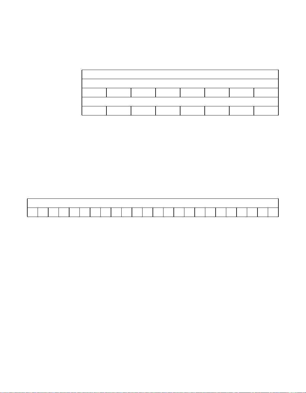
Register: 0x08
Revision ID
Read Only
7 0
RID
LSI53C875E
00100110
LSI53C875
00000100
RID Revision ID [7:0]
This register specifies device and revision identifiers. The
value of the LSI53C875E is 0x26 and 0x0 for the
LSI53C875.
Register: 0x09
Class Code
Read Only
23 0
CC
000011110000000000000000
CC Class Code [23:0]
This 24-bit register is used to identify the generic function
of the device. The upper byte of this register is a base
class code, the middle byte is a subclass code, and the
lower byte identifies a specific register level programming
interface. The value of this register is 0x010000, which
indicates a SCSI controller.
Configuration Registers 3-17
Page 82

Register: 0x0C
Cache Line Size
Read/Write
7 0
CLS
00000000
CLS Cache Line Size [7:0]
This register specifies the system cache line size in units
of 32-bit words. Cache mode is enabled and disabled by
the Cache Line Size Enable (CLSE) bit, bit 7 in the DMA
Control (DCNTL) register. Setting this bit causes the
LSI53C875 to align to cache line boundaries before
allowing any bursting, except during Memory Moves in
which the read and write addresses are not aligned to a
burst size boundary. For more information on this register,see the section Section 3.2.1, “Support for PCI Cache
Line Size Register.”
Register: 0x0D
Latency Timer
Read/Write
7 0
00000000
LT Latency Timer [7:0]
The Latency Timer register specifies, in units of PCI bus
clocks, the value of the Latency Timer for this PCI bus
master. The LSI53C875 supports this timer. All eight bits
are writable, allowing latency values of 0–255 PCI clocks.
Use the following equation to calculate an optimum
latency value for the LSI53C875:
Latency = 2 + (Burst Size x (typical wait states +1))
Values greater than optimum are also acceptable.
3-18 PCI Functional Description
LT
Page 83
Register: 0x0E
Header Type
Read Only
7 0
HT
00000000
HT Header Type [7:0]
This register identifies the layout of bytes 0x10 through
0x3F in configuration space and also whether or not the
device contains multiple functions. The value of this
register is 0x00.
Register: 0x10
Base Address Zero (I/O)
Read/Write
31 0
BAR0
xxxxxxxxxxxxxxxxxxxxxxxxxxxxxxx1
BAR0 Base Address Register Zero (I/O) [31:0]
This 32-bit register has bit zero hardwired to one. Bit 1 is
reserved and must return a zero on all reads, and the
other bits are used to map the device into I/O space.
Register: 0x14
Base Address One (Memory)
Read/Write
31 0
BAR1
xxxxxxxxxxxxxxxxxxxxxxxxxxxxxxx0
BAR1 Base Address Register One [31:0]
This register has bit 0 hardwired to zero. For detailed
information on the operation of this register, refer to the
PCI Specification.
Configuration Registers 3-19
Page 84

Register: 0x18
RAM Base Address Two (Memory) SCRIPTS RAM
Read/Write
31 0
BAR2
xxxxxxxxxxxxxxxxxxxxxxxxxxxxxxx0
BAR2 Base Address Register Two [31:0]
This register holds the memory base address of the
4 Kbyte internal RAM. Read this register through the
Scratch Register B (SCRATCHB) register in the operating
register set when bit 3 of the Chip Test Two (CTEST2)
register is set.
Register: 0x2C
Subsystem Vendor ID (SSVID)
Read Only
15 0
SSVID
LSI53C875E
1111000000000000
LSI53C875
0000000000000000
SSVID Subsystem Vendor ID [15:0]
This register supports subsystem identification, which has
a default value of 0x0000 in the LSI53C875 and 0x1000
in the LSI53C875E (see Section 4.1, “MAD Bus Program-
ming”). To write to this register, connect a 4.7 kΩ resistor
between the MAD[6] pin and Vssand leave the MAD[4]
pin unconnected. The MAD[6] and MAD[4] pins have
internal pull-up resistors and are sensed shortly after the
deassertion of chip reset. In revisions before Revision G
of the LSI53C875, the MAD[6] and MAD[4] pins do not
support the SSID and SSVID configurations, and only
values of 0x0000 can be found in the Subsystem Data
register.
3-20 PCI Functional Description
Page 85
Register: 0x2E
Subsystem ID (SSID)
Read Only
15 0
SSID
LSI53C875E
1111000000000000
LSI53C875
0000000000000000
SSID Subsystem ID [15:0]
This register supports subsystem identification, which has
a default value of 0x0000 in the LSI53C875 and 0x1000
in the LSI53C875E (see Section 4.1, “MAD Bus Program-
ming”). To write to this register, connect a 4.7 kΩ resistor
between the MAD[6] pin and Vssand leave the MAD[4]
pin unconnected. The MAD[6] and MAD[4] pins have
internal pull-up resistors and are sensed shortly after the
deassertion of chip reset. In revisions before Revision G
of the LSI53C875, the MAD[6] and MAD[4] pins do not
support the SSID and SSVID configurations, and only
values of 0x0000 can be found in the Subsystem Data
register.
Register: 0x30
Expansion ROM Base Address
Read/Write
31 0
ERBA
00000000000000000000000000000000
ERBA Expansion ROM Base Address [31:0]
This four-byte register handles the base address and size
information for expansion ROM. It functions exactly like
the Base Address Zero (I/O) and Base Address One
(Memory) registers, except that the encoding of the bits
is different. The upper 21 bits correspond to the upper
21 bits of the expansion ROM base address.
Configuration Registers 3-21
Page 86

The Expansion ROM Enable bit, bit 0, is the only bit
defined in this register. This bit is used to control whether
or not the device accepts accesses to its expansion
ROM. When the bit is set, address decoding is enabled,
and a device can be used with or without an expansion
ROM depending on the system configuration. To access
the external memory interface, also set the Memory
Space bit in the Command register.
The host system detects the size of the external memory
by first writing the Expansion ROM Base Address register
with all ones and then reading back the register. The
LSI53C875 responds with zeros in all don’t care
locations. The ones in the remaining bits represent the
binary version of the external memory size. For example,
to indicate an external memory size of 32 Kbytes, this
register, when written with ones and read back, returns
ones in the upper 17 bits.
Register: 0x34
Capabilities Pointer
Read Only
7 0
CP
01000000
CP Capabilities Pointer [7:0]
This register provides an offset into the function’s PCI
Configuration Space for the location of the first item in the
capabilities linked list. Only the LSI53C875E sets this
register to 0x40. The capability pointer replaces the
General Purpose Pin Control (GPCNTL) register in
earlier revisions of the LSI53C875.
3-22 PCI Functional Description
Page 87

Register: 0x3C
Interrupt Line
Read/Write
7 0
IL
00000000
IL Interrupt Line [7:0]
This register is used to communicate interrupt line routing
information. POST software writes the routing information
into this register as it configures the system. The value in
this register tells which input of the system interrupt
controller(s) the device’s interrupt pin is connected to.
Values in this register are specified by system
architecture.
Register: 0x3D
Interrupt Pin
Read Only
7 0
IP
00000001
IP Interrupt Pin [7:0]
This register tells which interrupt pin the device uses. Its
value is set to 0x01, for the INTA/ signal.
Configuration Registers 3-23
Page 88

Register: 0x3E
Min_Gnt
Read Only
7 0
MG
00010001
MG Min_Gnt [7:0]
This register is used to specify the desired settings for
latency timer values. Min_Gnt is used to specify how long
a burst period the device needs. The value specified in
these registers is in units of 0.25 microseconds. The
LSI53C875 sets this register to 0x11.
Register: 0x3F
Max_Lat
Read Only
7 0
ML
01000000
ML Max_Lat [7:0]
This register is used to specify the desired settings for
latency timer values. Max_Lat is used to specify how
often the device needs to gain access to the PCI bus.
The value specified in this register is in units of
0.25 microseconds. Values of zero indicate that the
device has no major requirements for the settings of
latency timers. The LSI53C875 sets this register to 0x40.
3-24 PCI Functional Description
Page 89
Register: 0x40
Capability ID
Read Only
7 0
CID
00000001
CID Cap_ID [7:0]
This register indicates the type of data structure currently
being used. It is set to 0x01, indicating the Power
Management Data Structure. Only the LSI53C875E sets
this register to 0x01.
Register: 0x41
Next Item Pointer
Read Only
7 0
NIP
00000000
NIP Next_Item_Ptr [7:0]
Bits [7:0] contain the offset location of the next item in the
controller capabilities list. The default value for this
register is 0x00, indicating that power management is the
last capability in the linked list of extended capabilities.
This register applies to the LSI53C875E only.
Register: 0x42
Power Management Capabilities
Read Only
15 11 10 9 8 6 5 4 3 2 0
PMES[4:0] D2S D1S
0 000 0 0 0 0 0 000 0 111
This register applies to the LSI53C875E only and indicates the power
management capabilities.
Configuration Registers 3-25
R DSI APS PMEC VER[2:0]
Page 90

PMES PME Support [15:11]
This field is always set to 00000b because the
LSI53C875E does not provide a PME signal.
D2S D2 Support 10
This device does not support the D2 power management
state, and this bit is set to zero.
D1S D1 Support 9
This device does not support the D1 power management
state, and this bit is set to zero.
R Reserved [8:6]
DSI Device Specific Initialization 5
This bit is set to 0 to indicate that the device requires no
special initialization before the generic class device driver
is able to use it.
APS Auxiliary Power Source 4
Because the device does not provide a PME signal, this
bit always returns a 0. This indicates that no auxiliary
power source is required to support the PME signal in the
D3cold power management state.
PMEC PME Clock 3
This bit always returns a zero value because the devices
do not provide a PME signal.
VER Version [2:0]
This field is set to 001b to indicate that the device
complies with Revision 1.0 of the PCI Power
Management Interface Specification.
Register: 0x44
Power Management Control/Status
Read/Write
15 14 13 12 9 8 7 2 1 0
PST DSCL DSLT PEN R PWS
000000000 0 0 0 0 000
This register applies to the LSI53C875E only and indicates the power
management control and status descriptions.
3-26 PCI Functional Description
Page 91

PST PME Status 15
The device always returns a zero for this bit, indicating
that PME signal generation is not supported from D3cold.
DSCL Data Scale [14:13]
This device does not support the Data register.
Therefore, this field is always set to 00b.
DSLT Data Select [12:9]
This device does not support the Data register.
Therefore, this field is always set to 0000b.
PEN PME Enable 8
This device always returns a zero for this bit to indicate
that PME assertion is disabled.
R Reserved [7:2]
PWS Power State [1:0]
This two bit field determines the current power state for
the function and is used to set the function to a new
power state. The definition of the field values are:
0b00 D0
0b01 Reserved
0b10 Reserved
0b11 D3 hot
Register: 0x46
Bridge Support Extensions (PMCSR_BSE)
Read Only
7 0
BSE
00000000
BSE Bridge Support Extensions [7:0]
This register applies to the LSI53C875E only and can
support PCI bridge specific functionality, if required. The
default value always returns 0x00.
Configuration Registers 3-27
Page 92

Register: 0x47
Data
Read Only
7 0
DATA
00000000
DATA Data [7:0]
This register applies to the LSI53C875E only and
provides an optional mechanism for the function to report
state dependent operating data. The LSI53C875E returns
0x00 as the default value.
3-28 PCI Functional Description
Page 93

Chapter 4
Signal Descriptions
This chapter presents the LSI53C875 pin configuration and signal
definitions using tables and illustrations. Figure 4.1 through Figure 4.4
are the pin diagrams for all versions of the LSI53C875 and Figure 4.5 is
the functional signal grouping. The pin definitions are presented in
Table 4.1 through Table 4.12. The LSI53C875 is a pin-for-pin
replacement for the LSI53C825.
LSI53C875/875E PCI to Ultra SCSI I/O Processor 4-1
Page 94
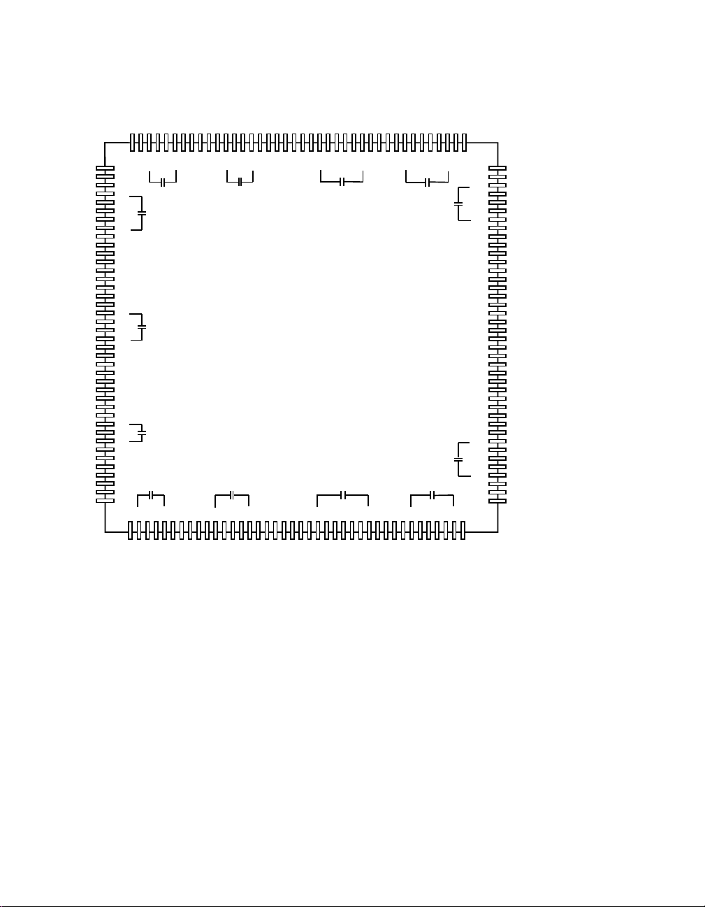
Figure 4.1 LSI53C875 Pin Diagram
SS-C
DD-C
SS
DD-I
SS
AD29
AD27
AD26
AD24
AD25
GNT/
V
AD31
AD30
AD28
V
V
V
REQ/
BIG_LIT/
CLK
V
RST/
SERR/
MCE/
MOE/
V
MWE/
DD
MAS1/
MAS0/
SDIR13
VSSSDIR12
SDIR15
SDIR14
SDIR0
SDIRP1
DD
V
SDIR1
SDIR2
SDIR4
VSSSDIR3
SDIR6
SDIR5
C_BE3/
IDSEL
AD23
V
AD22
AD21
AD20
V
DD-I
AD19
V
AD18
AD17
AD16
V
C_BE2/
FRAME/
IRDY/
V
TRDY/
DEVSEL/
V
DD-I
STOP/
V
PERR/
PAR/
C_BE1/
V
AD15
AD14
AD13
V
AD12
V
DD-I
AD11
AD10
AD9
V
AD8
C_BE0/
AD7
160
1
2
3
4
SS
5
6
7
8
9
10
SS
11
12
13
14
SS
15
16
17
18
SS
19
20
21
22
23
SS
24
25
26
27
SS
28
29
30
31
SS
32
33
34
35
36
37
SS
38
39
40
4143454749515355575961636567697173757677787980
AD6
155
157
159
4244464850525456586062646668707274
SS
V
AD5
158
AD4
154
156
DD-I
AD2
AD3
V
149
151
153
152
150
148
PCI to SCSI I/O Processor
SS
V
AD0
AD1
DD-C
IRQ/
V
GPIO0_FETCH/
GPIO1_MASTER/
142
143
144
145
146
147
LSI53C875
160-Pin
Quad Flat Pack
(Top View)
SS-C
V
SCLK
MAD7
MAD6
TESTIN
MAC/_TESTOUT
141
140
MAD5
139
MAD4
136
138
135
137
DD
V
MAD2
MAD1
MAD3
132
134
133
SS
V
MAD0
GPIO3
GPIO2_MAS2/
131
130
GPIO4
129
DIFFSENS
128
TGS
124
126
123
125
127
DD
IGS
V
SELDIR
RSTDIR
BSYDIR
Note: The decoupling capacitor arrangement shown above is recommended to maximize
the benefits of the internal split ground system. Capacitor values between 0.01 and
0.1 µF should provide adequate noise isolation. Because of the number of high
current drivers on the LSI53C875, a multilayer PC board with power and ground
planes is required.
122
SS
V
121
120
119
118
117
116
115
114
113
112
111
110
109
108
107
106
105
104
103
102
101
100
99
98
97
96
95
94
93
92
91
90
89
88
87
86
85
84
83
82
81
SDIR11
SDIR7
SDIRP0
V
DD
SD12/
SD13/
SD14/
V
SS-S
SD15/
SDP1/
SD0/
SD1/
V
SS-S
SD2/
SD3/
SD4/
SD5/
V
SS-S
SD6/
SD7/
SDP0/
SATN/
V
SS-S
SBSY/
SACK/
SRST/
SMSG/
SSEL/
V
SS-S
SC_D/
SREQ/
SI_O/
SD8/
V
SS-S
SD9/
SD10/
SD11/
V
DD
SDIR8
SDIR9
SDIR10
4-2 Signal Descriptions
Page 95

Figure 4.2 LSI53C875J Pin Diagram
SS-C
DD-C
SS
DD-I
SS
AD24
AD25
AD29
AD28
V
AD27
AD26
V
V
AD30
AD31
GNT/
V
REQ/
TDI
CLK
V
RST/
SERR/
MCE/
MWE/
VDDMOE/
MAS1/
MAS0/
VSSSDIR12
SDIR13
SDIR15
SDIR14
TCK
SDIR0
V
DD
SDIR1
SDIR2
VSSSDIR3
SDIR4
SDIR5
SDIR6
C_BE3/
IDSEL
AD23
V
AD22
AD21
AD20
V
DD-I
AD19
V
AD18
AD17
AD16
V
C_BE2/
FRAME/
IRDY/
V
TRDY/
DEVSEL/
V
DD-I
STOP/
V
PERR/
PAR/
C_BE1/
V
AD15
AD14
AD13
V
AD12
V
DD-I
AD11
AD10
AD9
V
AD8
C_BE0/
AD7
160
158
157
159
1
2
3
4
SS
5
6
7
8
9
10
SS
11
12
13
14
SS
15
16
17
18
SS
19
20
21
22
23
SS
24
25
26
27
SS
28
29
30
31
SS
32
33
34
35
36
37
SS
38
39
40
4143454749515355575961636567697173757677787980
4244464850525456586062646668707274
SS
V
AD6
AD5
AD4
152
154
156
153
155
SS
DD-I
V
AD2
AD3
AD1
V
147
148
150
149
151
LSI53C875J (JTAG)
PCI to SCSI I/O Processor
Quad Flat Pack
DD-C
IRQ/
V
GPIO0_FETCH/
SS-C
V
GPIO1_MASTER/
AD0
143
144
145
146
142
160-Pin
(Top View)
TMS
TDO
SCLK
MAD7
141
MAD5
MAD6
140
139
MAD4
135
137
134
136
138
DD
V
MAD2
MAD0
MAD1
MAD3
131
133
130
132
SS
V
GPIO4
GPIO3
DIFFSENS
GPIO2_MAS2/
129
128
TGS
123
125
127
122
124
126
IGS
SELDIR
RSTDIR
SS
V
BSYDIR
DD
V
Note: The decoupling capacitor arrangement shown above is recommended to maximize
the benefits of the internal split ground system. Capacitor values between 0.01 and
0.1 µF should provide adequate noise isolation. Because of the number of high
current drivers on the LSI53C875, a multilayer PC board with power and ground
planes is required.
121
120
119
118
117
116
115
114
113
112
111
110
109
108
107
106
105
104
103
102
101
100
99
98
97
96
95
94
93
92
91
90
89
88
87
86
85
84
83
82
81
SDIR11
SDIR7
SDIRP0
V
DD
SD12/
SD13/
SD14/
V
SS-S
SD15/
SDP1/
SD0/
SD1/
V
SS-S
SD2/
SD3/
SD4/
SD5/
V
SS-S
SD6/
SD7/
SDP0/
SATN/
V
SS-S
SBSY/
SACK/
SRST/
SMSG/
SSEL/
V
SS-S
SC_D/
SREQ/
SI_O/
SD8/
V
SS-S
SD9/
SD10/
SD11/
V
DD
SDIR8
SDIR9
SDIR10
4-3
Page 96
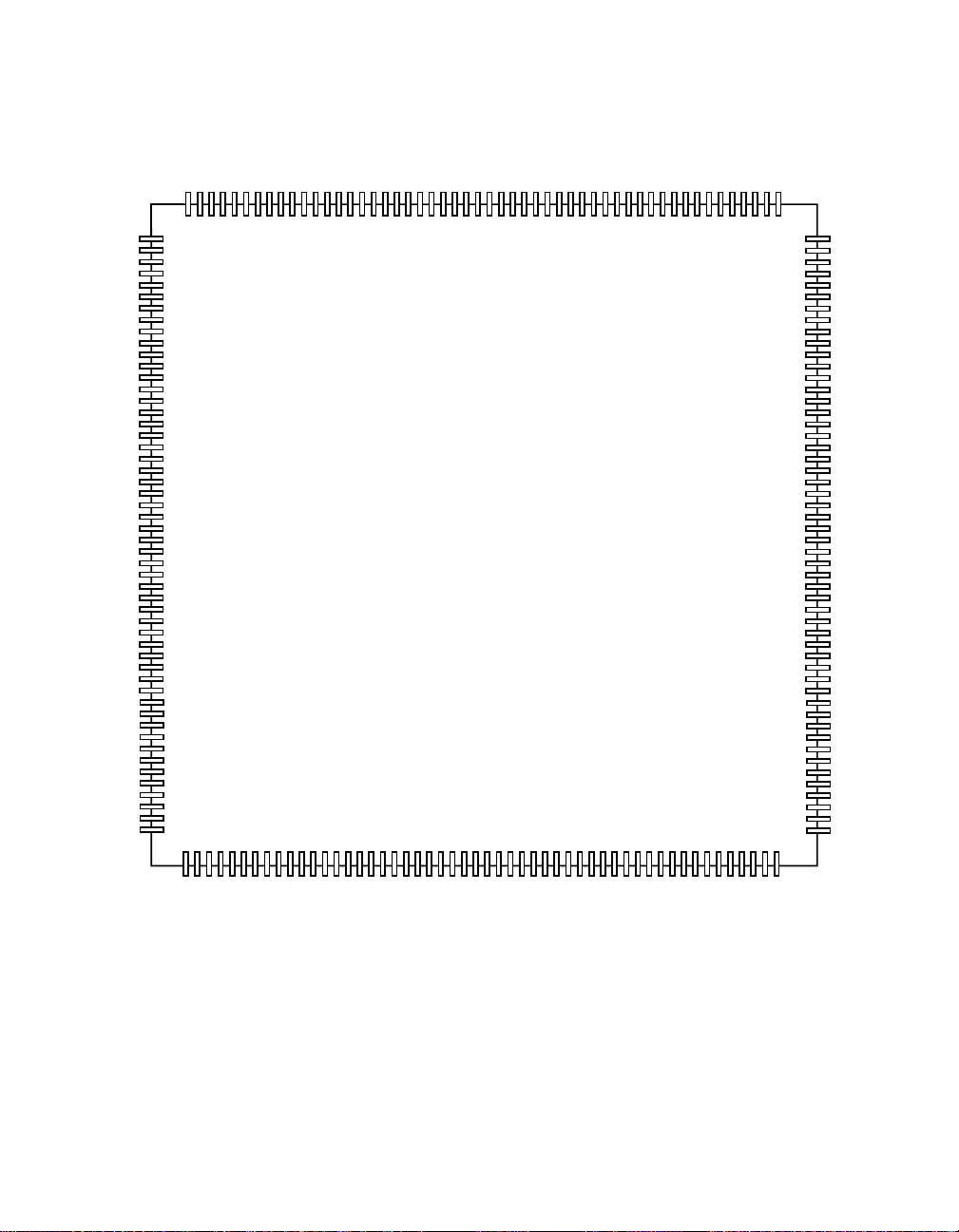
Figure 4.3 LSI53C875N Pin Diagram
DD-I
SS
AD26
V
AD24
NC
NC
NC
AD25
NC
AD27
SS
AD31
AD30
AD29
AD28
V
V
BYTEPAR3
DD-C
V
REQ/
GNT/
V
SS-C
CLK
RST/
SERR/
TDI
MCE/
BIG_LIT/
MOE/
MWE/
V
DD
MAS1
MAS0/
SDIR12
VSSSDIR13
SDIR15
SDIR14
TCK
SDIRP1
SDIR0
DD
V
SDIR2
SDIR1
SDIR3
SDIR4
V
SS
SDIR6
SDIR5
NC
NC
NC
NC
NC
C_BE3/
IDSEL
BYTEPAR2
AD23
V
AD22
AD21
AD20
V
DD-I
AD19
V
AD18
AD17
AD16
V
C_BE2/
FRAME/
IRDY/
V
TRDY/
DEVSEL/
V
DD-I
STOP/
V
PERR/
PAR
C_BE1/
V
BYTEPAR1
AD15
AD14
AD13
V
AD12
V
DD-I
AD11
AD10
AD9
V
AD8
C_BE0/
BYTEPAR0
AD7
208
204
206
203
205
207
1
NC
2
NC
NC
3
4
NC
NC
5
6
7
8
9
10
SS
11
12
13
14
15
16
SS
17
18
19
20
SS
21
22
23
24
SS
25
26
27
28
29
SS
30
31
32
33
SS
34
35
36
37
38
SS
39
40
41
42
43
44
SS
45
46
47
48
49
NC
50
NC
51
NC
52
NC
5355575961636567697173757779818385878889909192
5456586062646668707274767880828486
202
201
200
199
198
197
196
195
194
193
192
187
189
191
190
188
186
LSI53C875N
PCI to SCSI I/O Processor
208-Pin
Quad Flat Pack
185
184
183
182
181
180
179
178
177
176
175
174
173
172
171
169
170
165
167
166
168
93959799100
949698
164
163
162
161
101
160
102
159
103
158
104
157
156
156
155
155
154
154
153
153
152
152
151
151
150
150
149
149
148
148
147
147
146
146
145
145
144
144
143
143
142
142
141
141
140
140
139
139
138
138
137
137
136
136
135
135
134
134
133
133
132
132
131
131
130
130
129
129
128
128
127
127
126
126
125
125
124
124
123
123
122
122
121
121
120
120
119
119
118
118
117
117
116
115
114
113
112
111
110
109
108
107
106
105
NC
NC
NC
NC
NC
NC
SDIR7
SDIRP0
V
DD
SD12/
SD13
SD14/
V
SS-S
SD15/
SDP1/
SD0/
SD1/
V
SS-S
SD2/
SD3/
SD4/
SD5/
V
SS-S
SD6/
SD7/
SDP0/
SATN/
V
SS-S
SBSY/
SACK/
SRST/
SMSG/
SSEL/
V
SS-S
SC_D/
SREQ/
SI_0/
SD8/
V
SS-S
SD9/
SD10/
SD11/
V
DD
SDIR8
SDIR9
SDIR10
NC
NC
NC
NC
NC
NC
NCNCNC
NC
NC
AD6
SS
V
AD5
AD4
SS
DD-I
V
AD3
AD0
AD2
AD1
DD-C
V
IRQ/
V
GPIO0_FETCH
Note: The decoupling capacitor arrangement shown in Figures 4.1 and 4.2 is recom-
mended to maximize the benefits of the internal split ground system. Capacitor values between 0.01 and 0.1 µF should provide adequate noise isolation. Because of
the number of high current drivers on the LSI53C875, a multilayer PC board with
power and ground planes is required.
4-4 Signal Descriptions
SS-C
TMS
V
SCLK
TESTIN
GPIO1_MASTER/
MAC/_TESTOUT
TD0
MAD7
MAD6
MAD5
MAD4
V
DD
MAD3
MAD2
MAD1
MAD0
SS
V
GPIO3
GPIO4
DIFFSENS
GPIO2_MAS2/
TGS
IGS
SELDIR
RSTDIR
SS
V
BSYDIR
NC
SDIR11
NC
NCNCNC
DD
V
Page 97

Figure 4.4 LSI53C875JB Pin Diagram (Top View)
A1 A2 A3 A4 A5 A6 A7 A8 A9 A10 A11 A12 A13
C_BE3/ AD24 AD27 AD29 VDD-C CLK MCE/ MAS0/ VSS TCK SDIR2 SDIR5 SDIR6
B1 B2 B3 B4 B5 B6 B7 B8 B9 B10 B11 B12 B13
IDSEL NC VSS AD28 AD31 RST/ MDE/ MAS1/ SDIR14 VDD VSS NC SDIR7
C1 C2 C3 C4 C5 C6 C7 C8 C9 C10 C11 C12 C13
AD21 AD23 VSS AD26 AD30 VSS-C MWE/ SDIR12 SDIR15 SDIR1 SDIR4 VDD-S SD13/
D1 D2 D3 D4 D5 D6 D7 D8 D9 D10 D11 D12 D13
VSS VDD-1 AD20 AD25 VDD-1 GNT/ TDI SDIR13 SDIR0 SDIRP0 SD12 VSS-S SD15/
E1 E2 E3 E4 E5 E6 E7 E8 E9 E10 E11 E12 E13
AD16 AD17 AD18 AD19 AD22 REQ/ SERR/ VDD SDIR3 SD14/ SD0/ SD1/ VSS-S
F1 F2 F3 F4 F5 F6 F7 F8 F9 F10 F11 F12 F13
IRDY/ FRAME/ C_BE2/ VSS VSS VSS NC SDP1/ SD2/ SD3/ SD4/ VSS-S SD5/
G1 G2 G3 G4 G5 G6 G7 G8 G9 G10 G11 G12 G13
VDD DEVSEL/ TRDY/ STOP/ VSS NC NC NC SD6/ SD7/ VSS-S SATN/ SDP0/
H1 H2 H3 H4 H5 H5 H7 H8 H9 H10 H11 H12 H13
PAR PERR/ C-BE1/ VSS AD15 AD12 NC DIFFSENS SBSY/ SSEL/ SMSG/ SRST/ SACK/
J1 J2 J3 J4 J5 J6 J7 J8 J9 J10 J11 J12 J13
AD14 AD13 VSS AD10 VDD-1 TD0 VDD
K1 K2 K3 K4 K5 K6 K7 K8 K9 K10 K11 K12 K13
VDD-1 AD11 VSS C_BE0/ AD1
L1 L2 L3 L4 L5 L6 L7 L8 L9 L10 L11 L12 L13
GPIO1_
MASTER/ MAD4 MAD0 IGS VSS SD9/ VSS-S SI_0/
GPIO_
MAS2/ SD11/ SD8/ SREQ/ SC_D/ VSS-S
4-5
AD9 AD8 AD4 AD2 VDD-C VSS-C MAD7 MAD1 GPIO4 RSTDIR VDD-S SDIR8 SD10/
M1 M2 M3 M4 M5 M6 M7 M8 M9 M10 M11 M12 M13
AD7 NC AD5 VSS IRQ/ SCLK MAD6 MAD3 GPIO3 VDD BSYDIR NC SDIR9
N1 N2 N3 N4 N5 N6 N7 N8 N9 N10 N11 N12 N13
AD6 VSS AD3 AD0
GPIO_
FETCH/ TMS MAD5 MAD2 VSS TGS SELDIR SDIR11 SDIR10
Note: Pins F7, G6, G7, G8, and H7 are connected to the die pad.
Page 98

The PCI/SCSI pin definitions are organized into the following functional
groups: System, Address/Data, Interface Control, Arbitration, Error
Reporting, SCSI, and Optional Interface. A slash (/) at the end of the
signal name indicates that the active state occurs when the signal is at
a LOW voltage. When the slash is absent, the signal is active at a HIGH
voltage.
There are four signal type definitions:
I Input, a standard input-only signal.
O Output, a standard output driver (typically a Totem Pole Output).
T/S 3-state, a bidirectional, 3-state input/output signal.
S/T/S Sustained 3-state, an active LOW 3-state signal owned and driven by
one and only one agent at a time.
4-6 Signal Descriptions
Page 99

Table 4.1 describes the LSI53C875, LSI53C875J, LSI53C875E, and
LSI53C875JE Power and Ground Signals group.
Table 4.1 LSI53C875, LSI53C875J, LSI53C875E, and LSI53C875JE
Power and Ground Signals
Name Pin No. Description
V
SS
4, 10, 14, 18, 23, 27,
31, 37, 42, 48, 69, 79,
Ground to the PCI I/O pins.
123, 133, 152, 158
V
DD
V
DD-I
V
-S 88, 93, 99, 104, 109,
SS
V
-C 55, 146 Ground to the internal logic core.
SS
V
-C 51, 149 Power supplies to the internal logic core.
DD
63, 74, 84, 118, 128,
138
1
8, 21, 33, 45, 155 V
114
Power supplies to the Standard I/O pins.
pad for PCI I/O pins.
DD
Ground to the SCSI bus I/O pins.
1. These pins can accept a VDDsource of 3.3 V or 5 V. All other VDDpins must
be supplied 5 V.
Table 4.2 describes the LSI53C875N Power and Ground Signals group.
Table 4.2 LSI53C875N Power and Ground Signals
Name Pin No. Description
V
SS
10, 16, 20, 24, 29, 33,
38, 44, 59, 65, 88, 98,
164, 175, 196, 202
Ground to the PCI I/O pins.
V
DD
V
DD-I
V
-S 118, 123, 129, 134,
SS
V
-C 72, 189 Ground to the internal logic core.
SS
V
-C 68, 192 Power supplies to the internal logic core.
DD
82, 93, 148, 169, 180 Power supplies to the Standard I/O pins.
1
14, 27, 62, 199 V
pad for PCI I/O pins.
DD
Ground to the SCSI bus I/O pins.
139, 144
1. These pins can accept a VDDsource of 3.3 V or 5 V. All other VDDpins must
be supplied 5 V.
4-7
Page 100

Table 4.3 describes the LSI53C875JB and LSI53C875JBE Power and
Ground Signals group.
Table 4.3 LSI53C875JB and LSI53C875JBE Power and Ground
Signals
Name Pin No. Description
V
SS
A9, B3, B11, C3, D1,
F4, F5, F6, G5, H4, J3,
Ground to the PCI I/O pins.
K3, K10, M4, N2, N9
V
DD
V
DD-I
V
-S C12, L11 Ground to the SCSI bus I/O pins.
DD
V
-C L6, C6 Ground to the internal logic core.
SS
V
-C A5, L5 Power supplies to the internal logic core.
DD
B10, E8, J7, M10 Power supplies to the Standard I/O pins.
1
D2, D5, G1, J5, K1 V
pad for PCI I/O pins.
DD
1. These pins can accept a VDDsource of 3.3 V or 5 V. All other VDDpins must
be supplied 5 V.
4-8 Signal Descriptions
 Loading...