

Page 1

TECHNICAL
MANUAL
LSI53C895A
PCI to Ultra2
SCSI Controller
Version 2.2
April 2001
®
S14028.B
Page 2

This document contains proprietary information of LSI Logic Corporation. The
information contained herein is not to be used by or disclosed to third parties
without the express written permission of an officer of LSI Logic Corporation.
LSI Logic products are not intended for use in life-support appliances, devices,
or systems. Use of any LSI Logic product in such applications without written
consent of the appropriate LSI Logic officer is prohibited.
Document DB14-000089-03, Fourth Edition (April 2001)
This document describes the LSI Logic LSI53C895A PCI to Ultra2 SCSI
Controller and will remain the official reference source for all revisions/releases
of this product until rescinded by an update.
To receive product literature, visit us at http://www.lsilogic.com.
LSI Logic Corporation reserves the right to make changes to any products herein
at any time without notice. LSI Logic does not assume any responsibility or
liability arising out of the application or use of any product described herein,
except as expressly agreed to in writing by LSI Logic; nor does the purchase or
use of a product from LSI Logic convey a license under any patent rights,
copyrights, trademark rights, or any other of the intellectual property rights of
LSI Logic or third parties.
Ultra SCSI is the term used by the SCSI Trade Association (STA) to describe
Fast-20 SCSI, as documented in the SCSI-3 Fast-20 Parallel Interface standard,
X3,277-199X.
Ultra2 SCSI is the term used by the SCSI Trade Association (STA) to describe
Fast-40 SCSI, as documented in the SCSI Parallel Interface-2 standard, (SPI-2)
X3710-1142D.
Copyright © 1998–2001 by LSI Logic Corporation. All rights reserved.
TRADEMARK ACKNOWLEDGMENT
The LSI Logic logo design, TolerANT, LVDlink, and SCRIPTS are registered
trademarks or trademarks of LSI Logic Corporation. All other brand and product
names may be trademarks of their respective companies.
SR/HH
ii
Page 3

Audience
Preface
This book is the primary reference and technical manual for the
LSI53C895A PCI to Ultra2 SCSI Controller. It contains a complete
functional description for the product and also includes complete physical
and electrical specifications.
This manual provides reference information on the LSI53C895A PCI to
Ultra2 SCSI Controller. It is intended for system designers and
programmers who are using this device to design an Ultra2 SCSI port for
PCI-based personal computers, workstations, servers or embedded
applications.
Organization
This document has the following chapters and appendixes:
• Chapter 1, General Description, includes general information about
the LSI53C895A.
• Chapter 2, Functional Description, describes the main functional
areas of the chip in more detail, including interfaces to the SCSI bus
and external memory.
• Chapter 3, Signal Descript ions, contains pin diagrams and signal
descriptions.
• Chapter 4, Registers, describes each bit in the operating registers,
and is organized by register address.
• Chapter 5, SCSI SCRIPTS Instruction Set, defines all of the SCSI
SCRIPTS instructions that are supported by the LSI53C895A.
Preface iii
Page 4

• Chapter 6, Electrical Specifications, contains the electrical
• Appendix A, Register Summary , is a register summary.
• Appendix B, External Memory Interface Diagram Examples,
Related Publications
For background information, please contact:
ANSI
11 W est 42nd Street
New York, NY 10036
(212) 642-4900
Ask for document number X3.131-199X (SCSI-2)
Global Engineering Documents
15 Inverness Way East
Englewood, CO 80112
(800) 854-7179 or (303) 397-7956 (outside U.S.) FAX (303) 397-2740
Ask for document number X3.131-1994 (SCSI-2); X3.253
(SCSI-3 Parallel Interface)
characteristics and AC timing diagrams.
contains sever al example interface drawings for connecting the
LSI53C895A to external ROMs.
ENDL Publications
14426 Black Walnut Court
Saratoga, CA 95070
(408) 867-6642
Document names: SCSI Bench Reference, SCSI Encyclopedia,
SCSI Tutor
Prentice Hall
113 Sylvan Avenue
Englewood Cliffs, NJ 07632
(800) 947-7700
Ask for document number ISBN 0-13-796855-8, SCSI: Understanding
the Small Computer System Interface
iv Preface
Page 5

LSI Logic World Wide Web Home Page
www.lsilogic.com
PCI Special Interest Group
2575 N.E. Katherine
Hillsboro, OR 97214
(800) 433-5177; (503) 693-6232 (International); FAX (503) 693-8344
Conventions Used in This Manual
The word assert means to drive a signal true or active . The word
deassert means to drive a signal false or inactive.
Hexadecimal numbers are indicated by the prefix “0x” —for example,
0x32CF. Binary numbers are indicated by the prefix “0b” —for example,
0b0011.0010.1100.1111.
Revision Record
Revision Date Remarks
0.5 4/99 Advance information version of the manual.
1.0 7/99 Preliminary version of the manual.
1.1 9/99 PCI timings corrected in Chapter 6, Table 6.3, and Figure 6.41 corrected.
2.0 2/00 Final version.
2.1 7/00 Added Figure 6.43.
2.2 4/01 All product names changed from SYM to LSI. Updated DC electrical
specifications and test conditions.
Preface v
Page 6

vi Preface
Page 7

Contents
Chapter 1 General Description
1.1 New Features in the LSI53C895A 1-3
1.2 Benefits of Ultra2 SCSI 1-4
1.3 Benefits of LVDlink 1-4
1.4 TolerANT
1.5 LSI53C895A Benefits Summary 1-6
1.5.1 SCSI Performance 1-6
1.5.2 PCI Performance 1-7
1.5.3 Integration 1-8
1.5.4 Ease of Use 1-8
1.5.5 Flexibility 1-9
1.5.6 Reliability 1-9
1.5.7 Testability 1-10
®
Technology 1-5
Chapter 2 Functional Description
2.1 PCI Functional Description 2-2
2.1.1 PCI Addressing 2-2
2.1.2 PCI Bus Commands and Functions Supported 2-4
2.1.3 PCI Cache Mode 2-9
2.2 SCSI Functional Description 2-18
2.2.1 SCRIPTS Processor 2-19
2.2.2 Internal SCRIPTS RAM 2-20
2.2.3 64-Bit Addressing in SCRIPTS 2-21
2.2.4 Hardware Control of SCSI Activity LED 2-21
2.2.5 Designing an Ultra2 SCSI System 2-22
2.2.6 Prefetching SCRIPTS Instructions 2-23
2.2.7 Opcode Fetch Burst Capability 2-24
2.2.8 Load and Store Instructions 2-24
2.2.9 JTAG Boundary Scan Testing 2-25
Contents vii
Page 8

2.2.10 SCSI Loopback Mode 2-26
2.2.11 Parity Options 2-26
2.2.12 DMA FIFO 2-29
2.2.13 SCSI Bus Interface 2-34
2.2.14 Select/Reselect During Selection/Reselection 2-39
2.2.15 Synchronous Operation 2-40
2.2.16 Interrupt Handling 2-43
2.2.17 Interrupt Routing 2-50
2.2.18 Chained Block Moves 2-51
2.3 Parallel ROM Interface 2-55
2.4 Serial EEPROM Interface 2-57
2.4.1 Default Download Mode 2-57
2.4.2 No Download Mode 2-58
2.5 Alternative SSVID/SSID Loading Mechanism 2-58
2.6 Power Management 2-60
2.6.1 Power State D0 2-61
2.6.2 Power State D1 2-61
2.6.3 Power State D2 2-62
2.6.4 Power State D3 2-62
Chapter 3 Signal Descriptions
3.1 LSI53C895A Functional Signal Grouping 3-2
3.2 Signal Descriptions 3-3
3.2.1 Internal Pull-ups on LSI53C895A Signals 3-3
3.3 PCI Bus Interface Signals 3-4
3.3.1 System Signals 3-4
3.3.2 Address and Data Signals 3-5
3.3.3 Interface Control Signals 3-6
3.3.4 Arbitration Signals 3-8
3.3.5 Error Reporting Signals 3-8
3.3.6 Interrupt Signals 3-9
3.3.7 SCSI GPIO Signals 3-10
3.4 SCSI Bus Interface Signals 3-11
3.4.1 SCSI Bus Interface Signal 3-11
3.4.2 SCSI Signals 3-12
3.4.3 SCSI Control Signals 3-13
3.5 Flash ROM and Memory Interface Signals 3-14
viii Contents
Page 9

3.6 Test Interface Signals 3-16
3.7 Power and Ground Signals 3-17
3.8 MAD Bus Programming 3-19
Chapter 4 Registers
4.1 PCI Configuration Registers 4-1
4.2 SCSI Registers 4-19
4.3 64-Bit SCRIPTS Selectors 4-104
4.4 Phase Mismatch Jump Registers 4-108
Chapter 5 SCSI SCRIPTS Instruction Set
5.1 Low Level Register Interface Mode 5-1
5.2 High Level SCSI SCRIPTS Mode 5-2
5.2.1 Sample Operation 5-3
5.3 Block Move Instruction 5-5
5.3.1 First Dword 5-6
5.3.2 Second Dword 5-12
5.4 I/O Instruction 5-13
5.4.1 First Dword 5-13
5.4.2 Second Dword 5-21
5.5 Read/Write Instructions 5-22
5.5.1 First Dword 5-22
5.5.2 Second Dword 5-23
5.5.3 Read-Modify-Write Cycles 5-23
5.5.4 Move To/From SFBR Cycles 5-24
5.6 Transfer Control Instructions 5-26
5.6.1 First Dword 5-26
5.6.2 Second Dword 5-32
5.7 Memory Move Instructions 5-32
5.7.1 First Dword 5-33
5.7.2 Read/Write System Memory from SCRIPTS 5-34
5.7.3 Second Dword 5-34
5.7.4 Third Dword 5-35
5.8 Load and Store Instructions 5-35
5.8.1 First Dword 5-36
5.8.2 Second Dword 5-37
Contents ix
Page 10

Chapter 6 Electrical Specifications
6.1 DC Characteristics 6-1
6.2 TolerANT Technology Electrical Characteristics 6-8
6.3 AC Characteristics 6-12
6.4 PCI and External Memory Interface Timing Diagrams 6-14
6.4.1 Target Timing 6-15
6.4.2 Initiator Timing 6-22
6.4.3 External Memory Timing 6-39
6.5 SCSI Timing Diagrams 6-56
6.6 Package Diagrams 6-64
6.6.1 LSI53C895A vs. LSI53C895 Pin/Ball Differences 6-71
Appendix A Register Summary
Appendix B External Memory Interface Diagram Examples
Index
Customer Feedback
Figures
1.1 Typical LSI53C895A System Application 1-2
1.2 Typical LSI53C895A Board Application 1-3
2.1 LSI53C895A Block Diagram 2-2
2.2 Parity Checking/Generation 2-29
2.3 DMA FIFO Sections 2-30
2.4 LSI53C895A Host Interface SCSI Data Paths 2-31
2.5 8-Bit HVD Wiring Diagram for Ultra2 SCSI 2-37
2.6 Regulated Termination for Ultra2 SCSI 2-39
2.7 Determining the Synchronous Transfer Rate 2-41
2.8 Block Move and Chained Block Move Instructions 2-52
3.1 LSI53C895A Functional Signal Grouping 3-2
5.1 SCRIPTS Overview 5-5
6.1 LVD Driver 6-3
6.2 LVD Receiver 6-4
xContents
Page 11

6.3 Rise and Fall Time Test Condition 6-9
6.4 SCSI Input Filtering 6-9
6.5 Hysteresis of SCSI Receivers 6-10
6.6 Input Current as a Function of Input Voltage 6-10
6.7 Output Current as a Function of Output Voltage 6-11
6.8 External Clock 6-12
6.9 Reset Input 6-13
6.10 Interrupt Output 6-14
6.11 PCI Configuration Register Read 6-16
6.12 PCI Configuration Register Write 6-17
6.13 32-Bit Operating Register/SCRIPTS RAM Read 6-18
6.14 64-Bit Address Operating Register/SCRIPTS RAM Read 6-19
6.15 32-Bit Operating Register/SCRIPTS RAM Write 6-20
6.16 64-Bit Address Operating Register/SCRIPTS RAM Write 6-21
6.17 Nonburst Opcode Fetch, 32-Bit Address and Data 6-23
6.18 Burst Opcode Fetch, 32-Bit Address and Data 6-25
6.19 Back to Back Read, 32-Bit Address and Data 6-27
6.20 Back to Back Write, 32-Bit Address and Data 6-29
6.21 Burst Read, 32-Bit Address and Data 6-31
6.22 Burst Read, 64-Bit Address and Data 6-33
6.23 Burst Write, 32-Bit Address and Data 6-35
6.24 Burst Write, 64-Bit Address and 32-Bit Data 6-37
6.25 External Memory Read 6-40
6.26 External Memory Write 6-44
6.27 Normal/Fast Memory (
≥ 128 Kbytes) Single Byte
Access Read Cycle 6-46
6.28 Normal/Fast Memory (
≥ 128 Kbytes) Single Byte
Access Write Cycle 6-47
6.29 Normal/Fast Memory (
≥ 128 Kbytes) Multiple Byte
Access Read Cycle 6-48
6.30 Normal/Fast Memory (
≥ 128 Kbytes) Multiple Byte
Access Write Cycle 6-50
6.31 Slow Memory (
6.32 Slow Memory (
6.33
6.34
≤ 64 Kbytes ROM Read Cycle 6-54
≤ 64 Kbyte ROM Write Cycle 6-55
≤ 128 Kbytes) Read Cycle 6-52
≤ 128 Kbytes) Write Cycle 6-53
6.35 Initiator Asynchronous Send 6-56
6.36 Initiator Asynchronous Receive 6-57
Contents xi
Page 12

Tables
6.37 Target Asynchronous Send 6-58
6.38 Target Asynchronous Receive 6-59
6.39 Initiator and T arget Synchronous Transfer 6-63
6.40 LSI53C895A 272-Pin BGA Top View 6-65
6.41 LSI53C895A 208-Pin Plastic Quad Flat Pack 6-68
6.42 LSI53C895A 208 PQFP Mechanical Drawing
(Sheet 1 of 2) 6-74
6.43 LSI53C895A 272 PBGA Mechanical Drawing 6-76
B.1 16KbyteInterfacewith200nsMemory B-1
B.2 64KbyteInterfacewith150nsMemory B-2
B.3 128 Kbytes, 256 Kbytes, 512 Kbytes, or 1 Mbyte
Interface with 150 ns Memory B-3
B.4 512 Kbyte Interface with 150 ns Memory B-4
2.1 PCI Bus Commands and Encoding Types for the
LSI53C895A 2-4
2.2 PCI Cache Mode Alignment 2-13
2.3 Bits Used for Parity Control and Generation 2-27
2.4 SCSI Parity Control 2-28
2.5 SCSI Parity Errors and Interrupts 2-28
2.6 HVD Signals 2-35
2.7 Parallel ROM Support 2-56
2.8 Mode A Serial EEPROM Data Format 2-58
2.9 Power States 2-61
3.1 LSI53C895A Internal Pull-ups 3-3
3.2 System Signals 3-4
3.3 Address and Data Signals 3-5
3.4 Interface Control Signals 3-6
3.5 Arbitration Signals 3-8
3.6 Error Reporting Signals 3-8
3.7 Interrupt Signals 3-9
3.8 SCSI GPIO Signals 3-10
3.9 SCSI Bus Interface Signal 3-11
3.10 SCSI Signals 3-12
3.11 SCSI Control Signals 3-13
3.12 Flash ROM and Memory Interface Signals 3-14
3.13 Test Interface Signals 3-16
xii Contents
Page 13

3.14 Power and Ground Signals 3-17
3.15 Decode of MAD Pins 3-20
4.1 PCI Configuration Register Map 4-2
4.2 SCSI Register Address Map 4-20
4.3 Examples of Synchronous Transfer Periods and Rates
for SCSI-1 4-33
4.4 Example Transfer Periods and Rates for Fast SCSI-2,
Ultra, and Ultra2 4-34
4.5 Maximum Synchronous Offset 4-35
4.6 SCSI Synchronous Data FIFO Word Count 4-45
5.1 SCRIPTS Instructions 5-3
5.2 SCSI Information Transfer Phase 5-11
5.3 Read/Write Instructions 5-24
5.4 Transfer Control Instructions 5-26
5.5 SCSI Phase Comparisons 5-29
6.1 Absolute Maximum Stress Ratings 6-2
6.2 Operating Conditions 6-2
6.3 LVD Driver SCSI Signals—SD[15:0]+, SDP[1:0]/, SREQ/,
SREQ2/, SACK/, SACK2/, SMSG/, SIO/, SCD/, SATN/,
SBSY/, SSEL/, SRST/ 6-3
6.4 LVD Receiver SCSI Signals—SD[15:0]/, SDP[1:0]/,
SREQ/, SREQ2/, SACK/, SACK2/, SMSG/, SIO/, SCD/,
SATN/, SBSY/, SSEL/, SRST/ 6-3
6.5 DIFFSENS SCSI Signal 6-4
6.6 Input Capacitance 6-4
6.7 Bidirectional Signals—MAD[7:0], MAS/[1:0], MCE/,
MOE/, MWE/ 6-5
6.8 Bidirectional Signals—GPIO0_FETCH/,
GPIO1_MASTER/, GPIO[2:8] 6-5
6.9 Bidirectional Signals—AD[31:0], C_BE[3:0]/, FRAME/,
IRDY/, TRDY/, DEVSEL/, STOP/, PERR/, PAR 6-6
6.10 InputSignals—CLK,GNT/,IDSEL,RST/,SCLK,TCK,
TDI, TEST_HSC, TEST_RST, TMS, TRST/ 6-6
6.11 Output Signal—TDO 6-7
6.12 Output Signals—ALT_IRQ/, IRQ/, MAC/_TESTOUT,
REQ/ 6-7
6.13 Output Signal—SERR/ 6-7
6.14 TolerANT Technology Electrical Characteristics for SE
SCSI Signals 6-8
Contents xiii
Page 14

6.15 External Clock 6-12
6.16 Reset Input 6-13
6.17 Interrupt Output 6-14
6.18 PCI Configuration Register Read 6-16
6.19 PCI Configuration Register Write 6-17
6.20 32-Bit Operating Register/SCRIPTS RAM Read 6-18
6.21 64-Bit Address Operating Register/SCRIPTS RAM Read 6-19
6.22 32-Bit Operating Register/SCRIPTS RAM Write 6-20
6.23 64-Bit Address Operating Register/SCRIPTS RAM Write 6-21
6.24 Nonburst Opcode Fetch, 32-Bit Address and Data 6-22
6.25 Burst Opcode Fetch, 32-Bit Address and Data 6-24
6.26 Back to Back Read, 32-Bit Address and Data 6-26
6.27 Back to Back Write, 32-Bit Address and Data 6-28
6.28 Burst Read, 32-Bit Address and Data 6-30
6.29 Burst Read, 64-Bit Address and Data 6-32
6.30 Burst Write, 32-Bit Address and Data 6-34
6.31 Burst Write, 64-Bit Address and 32-Bit Data 6-36
6.32 External Memory Read 6-39
6.33 External Memory Write 6-43
6.34 Normal/Fast Memory (
≥ 128 Kbytes) Single Byte Access
Read Cycle 6-46
6.35 Normal/Fast Memory (
≥ 128 Kbytes) Single Byte Access
Write Cycle 6-47
6.36 Slow Memory (
6.37 Slow Memory (
6.38
6.39
≤= 64 Kbytes ROM Read Cycle 6-54
≤ 64 Kbyte ROM Write Cycle 6-55
≤ 128 Kbytes) Read Cycle 6-52
≤ 128 Kbytes) Write Cycle 6-53
6.40 Initiator Asynchronous Send 6-56
6.41 Initiator Asynchronous Receive 6-57
6.42 Target Asynchronous Send 6-58
6.43 Target Asynchronous Receive 6-59
6.44 SCSI-1 Transfers (SE 5.0 Mbytes) 6-59
6.45 SCSI-1 Transfers (Differential 4.17 Mbytes) 6-60
6.46 SCSI-2 Fast Transfers 10.0 Mbytes (8-Bit Transfers) or
20.0 Mbytes (16-Bit Transfers) 40 MHz Clock 6-60
6.47 SCSI-2 Fast Transfers 10.0 Mbytes (8-Bit Transfers) or
20.0 Mbytes (16-Bit Transfers) 50 MHz Clock 6-61
xiv Contents
Page 15

6.48 Ultra SCSI SE Transfers 20.0 Mbytes (8-Bit Transfers) or
40.0 Mbytes (16-Bit Transfers) Quadrupled 40 MHz Clock 6-61
6.49 Ultra SCSI High Voltage Differential Transfers 20.0 Mbytes
(8-Bit Transfers) or 40.0 Mbytes (16-Bit Transfers) 80 MHz
Clock 6-62
6.50 Ultra2 SCSI Transfers 40.0 Mbytes (8-Bit Transfers) or
80.0 Mbytes (16-Bit Transfers) Quadrupled 40 MHz Clock 6-63
6.51 272 BGA Pin List by Location 6-66
6.52 BGA Pin List Alphabetically 6-67
6.53 Signal Names vs. Pin Number: 208-Pin Plastic Quad
Flat Pack 6-69
6.54 LSI53C895A vs. LSI53C895 Pin/Ball Differences 6-72
A.1 LSI53C895A PCI Register Map A-1
A.2 LSI53C895A SCSI Register Map A-2
Contents xv
Page 16

xvi Contents
Page 17

Chapter 1
General Description
Chapter 1 is divided into the following sections:
• Section 1.1, “New Features in the LSI53C895A”
• Section 1.2, “Benefits of Ultra2 SCSI”
• Section 1.3, “Benefits of LVDlink”
• Section 1.4, “TolerANT® Technology”
• Section 1.5, “LSI53C895A Benefits Summary”
The LSI53C895A PCI to Ultra2 SCSI Controller brings Ultra2 SCSI
performance to host adapter, workstation, and general computer designs,
making it easy to add a high-performance SCSI bus to any PCI system.
It supports Ultra2 SCSI transfer rates and allows increased SCSI
connectivity and cable length with Low Voltage Differential (LVD)
signaling for SCSI devices. The LSI53C895A is packaged in a
208 Plastic Quad Flat Pack (PQFP) and a 272 Ball Grid Array (BGA).
The LSI53C895A can be used as a drop-in replacement for the
LSI53C895.
The LSI53C895A has a local memory bus for local storage of the
device’s BIOS ROM in flash memory or standard EEPROMs. The
LSI53C895A supports programming of local flash memory for updates to
BIOS. Appendix B, “External Memory Interface Diagram Examples,” has
system diagrams showing the connections of the LSI53C895A with an
external ROM or flash memory.
LVDlink™ technology is the LSI Logic implementation of LVD. LVDlink
transceivers allow the LSI53C895A to perform either Single-Ended (SE)
or LVD transfers. It also supports external High Voltage Differential (HVD)
transceivers. The LSI53C895A integrates a high-performance SCSI core,
a 64-bit PCI bus master DMA core, and the LSI Logic SCSI SCRIPTS™
processor to meet the flexibility requirements of SCSI-3 and Ultra2 SCSI
LSI53C895A PCI to Ultra2 SCSI Controller 1-1
Page 18
standards. It implements multithreaded I/O algorithms with a minimum of
processor intervention, solving the protocol overhead problems of
previous intelligent and nonintelligent adapter designs.
Figure 1.1 illustrates a typical LSI53C895A system and Figure 1.2
illustrates a typical LSI53C895A board application.
Figure 1.1 Typical LSI53C895A System Application
PCI Bus
Interface
Controller
Processor Bus
Central
Processing
Unit
(CPU)
PCI Bus
Typical PCI
Computer System
Architecture
LSI53C895A
PCItoWideUltra2
SCSI Controller
PCI Graphic Accelerator
PCI Fast Ethernet
Memory
Controller
Memory
SCSI Bus
Fixed Disk, Optical Disk
Printer, Tape, and Other
Peripherals
1-2 General Description
Page 19
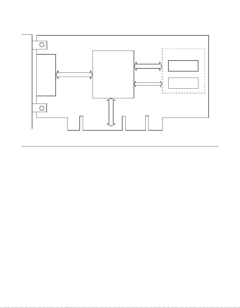
Figure 1.2 Typical LSI53C895A Board Application
SCSI Data,
Parity and
68 Pin
SCSI
Wide
Connector
Control
Signals
PCI Address, Data, Parity and Control Signals
LSI53C895A
32-Bit PCI to
SCSI Controller
PCI Interface
1.1 New Features in the LSI53C895A
The LSI53C895A is a drop-in replacement for the LSI53C895 PCI to
Ultra2 SCSI Controller, with these additional benefits:
• Supports 32-bit PCI Interface with 64-bit addressing.
Memory
Address/Data
Bus
GPIO[1:0]
Memory Control
Block
Flash EEPROM
Serial EEPROM
• Handles SCSI phase mismatches in SCRIPTS without interrupting
the CPU .
• Supports JTAG boundary scanning.
• Supports RAID ready alternative interrupt signaling.
• Supports PC99 Power Management.
– Automatically downloads Subsystem Vendor ID , Subsystem ID,
and PCI power management levels D0, D1, D2, and D3.
• Improves PCI bus efficiency through improved PCI caching design.
• Transfers Load/Store data to or from 8 Kbytes of internal SCRIPTS
RAM.
New Features in the LSI53C895A 1-3
Page 20

Additional features of the LSI53C895A include:
• Hardware control of SCSI activity LED.
• Nine GPIO Pins.
• 32-bit ISTAT registers (Interrupt Status Zero (ISTAT0), Interrupt
Status One (ISTAT1), Mailbox Zero (MBOX0), and Mailbox One
(MBOX1)).
• Optional 944 byte DMA FIFO supports large block transfers at Ultra2
SCSI speeds. The default FIFO size of 112 bytes is also supported.
1.2 Benefits of Ultra2 SCSI
Ultra2 SCSI is an extension of the SPI-2 draft standard that allows faster
synchronous SCSI transfer rates. It also defines a new physical layer,
LVD SCSI, that provides an incremental evolution from SCSI-2 and Ultra
SCSI. When enabled, Ultra2 SCSI performs 40 megatransfers per
second, resulting in approximately twice the synchronous transfer rates
of Ultra SCSI. The LSI53C895A can perform 16-bit, Ultra2 SCSI
synchronous transfers as fast as 80 Mbytes/s. This advantage is most
noticeable in heavily loaded systems or with applications with large block
requirements, such as video on-demand and image processing.
An advantage of Ultra2 SCSI is that it significantly improves SCSI
bandwidth while preserving existing hardware and software investments.
The primary software changes required enable the chip to perform
synchronous negotiations for Ultra2 SCSI rates and to enable the clock
quadrupler. Ultra2 SCSI uses the same connectors as Ultra SCSI, but
can operate with longer cables and more devices on the bus.
Chapter 2, “Functional Description,” contains more information on
migrating an Ultra SCSI design to support Ultra2 SCSI.
1.3 Benefits of LVDlink
The LSI53C895A supports LVD for SCSI. This signaling technology
increases the reliability of SCSI data transfers over longer distances than
are supported by SE SCSI. The low current output of LVD allows the I/O
transceivers to be integrated directly onto the chip. LVD provides the
reliability of HVD SCSI without the added cost of external differential
1-4 General Description
Page 21

transceivers. Ultra2 SCSI with LVD allows a longer SCSI cable and more
devices on the bus, with the same cables defined in the SCSI-3 Parallel
Interface standard for Ultra SCSI. LVD provides a long-term migration
path to even faster SCSI transfer rates without compromising signal
integrity , cable length, or connectivity.
For backward compatibility to existing SE devices, the LSI53C895A
features universal LVDlink transceivers that can support LVD SCSI, SE,
and HVD modes. The LVDlink technology also supports HVD signaling
in legacy systems when external transceivers are connected to the
LSI53C895A. This allows use of the LSI53C895A in both legacy and
Ultra2 SCSI applications.
1.4 TolerANT®Technology
The LSI53C895A features TolerANT technology, which includes active
negation on the SCSI drivers and input signal filtering on the SCSI
receivers. Active negation actively drives the SCSI Request,
Acknowledge, Data, and Parity signals HIGH rather than allowing them
to be passively pulled up by terminators. Active negation is enabled by
setting bit 7 in the SCSI Test Three (STEST3) register.
TolerANT receiver technology improves data integrity in unreliable
cabling environments where other devices would be subject to data
corruption. TolerANT receivers filter the SCSI bus signals to eliminate
unwanted transitions, without the long signal delay associated with
RC-type input filters. This improved driver and receiver technology helps
eliminate double clocking of data, the single biggest reliability issue with
SCSI operations.
The benefits of TolerANT technology include increased immunity to noise
when the signal is going HIGH, better performance due to balanced duty
cycles, and improved fast SCSI transfer rates. In addition, TolerANT SCSI
devices do not cause glitches on the SCSI bus at power-up or
power-down, so other devices on the bus are also protected from data
corruption. When used with the LVDlink transceivers, TolerANT
technology provides excellent signal quality and data reliability in real
world cabling environments.TolerANT technology is compatible with both
the Alternative One and Alternative Two termination schemes proposed
by the American National Standards Institute.
TolerANT®Technology 1-5
Page 22

1.5 LSI53C895A Benefits Summary
This section of the chapter provides an overview of the LSI53C895A
features and benefits. It contains these topics:
• SCSI Performance
• PCI Performance
• Integration
• Ease of Use
• Flexibility
• Reliability
• Testability
1.5.1 SCSI Performance
To improve SCSI performance, the LSI53C895A:
• Has integrated LVDlink universal transceivers which:
– Support SE, LVD, and HVD signals (with external transceivers).
– Allow greater device connectivity and longer cable length.
– Save the cost of external differential transceivers.
– Support a long-term performance migration path.
• Bursts up to 512 bytes across the PCI bus through its 944 byte FIFO.
• Performs wide, Ultra2 SCSI synchronous transfers as fast as
80 Mbytes/s.
• Can handle phase mismatches in SCRIPTS without interrupting the
system processor, eliminating the need for CPU intervention during
an I/O disconnect/reselect sequence.
• Achieve Ultra2 SCSI transfer rates with an input frequency of 40 MHz
with the on-chip SCSI clock quadrupler .
• Includes 8 Kbytes internal RAM for SCRIPTS instruction storage.
• Has 31 levels of SCSI synchronous offset.
• Supports variable block size and scatter/gather data transfers.
1-6 General Description
Page 23

• Performs sustained memory-to-memory DMA transfers to
approximately 100 Mbytes/s.
• Minimizes SCSI I/O start latency.
• Performs complex bus sequences without interrupts, including
restoring data pointers.
• Reduces ISR overhead through a unique interrupt status reporting
method.
• Uses Load/Store SCRIPTS instructions which increase performance
of data transfers to and from the chip registers without using PCI
cycles.
• Has SCRIPTS support for 64-bit addressing.
• Supports multithreaded I/O algorithms in SCSI SCRIPTS with fast
I/O context switching.
• Supports additional arithmetic capability with the Expanded Register
Move instruction.
1.5.2 PCI Performance
To improve PCI performance, the LSI53C895A:
• Complies with PCI 2.2 specification.
• Supports 32-bit 33 MHz PCI interface with 64-bit addressing.
• Supports dual address cycles which can be generated for all
SCRIPTS for > 4 Gbyte addressability.
• Bursts 2, 4, 8, 16, 32, 64, or 128 Dword transfers across the PCI bus.
• Supports 32-bit word data bursts with variable burst lengths.
• Prefetches up to 8 Dwords of SCRIPTS instructions.
• Bursts SCRIPTS opcode fetches across the PCI bus.
• Perf orms zero wait-state bus master data bursts faster than
110 Mbytes/s (@ 33 MHz).
• Supports PCI Cache Line Size register.
• Supports PCI Write and Invalidate, Read Line, and Read Multiple
commands.
• Complies with PCI Bus Power Management Specification
Revision 1.1.
LSI53C895A Benefits Summary 1-7
Page 24

1.5.3 Integration
Features of the LSI53C895A which ease integration include:
• High-perfor mance SCSI core.
• Integrated LVD transceivers.
• Full 32-bit PCI DMA bus master.
• Integrated SCRIPTS processor.
• Memory-to-Memory Move instructions allow use as a third-party PCI
1.5.4 Ease of Use
The LSI53C895A provides:
• Easy, drop-in replacement for the LSI53C895.
• Up to one megabyte of add-in memory support for BIOS and
• Reduced SCSI development effort.
• Compiler-compatible with existing LSI53C7XX and LSI53C8XX
bus DMA controller.
SCRIPTS storage.
family SCRIPTS.
• Direct connection to PCI and SCSI SE, LVD and HVD (needs
external transceivers).
• Development tools and sample SCSI SCRIPTS available.
• Nine GPIO pins.
• Maskable and pollable interrupts.
• Wide SCSI, A or P cable, and up to 15 devices supported.
• Three programmable SCSI timers: Select/Reselect,
Handshake-to-Handshake, and General Purpose. The time-out
period is programmable from 100
• Software for PC-based operating system support.
• Support for relative jumps.
• SCSI Selected as ID bits for responding with multiple IDs.
1-8 General Description
µs to greater than 25.6 seconds.
Page 25

1.5.5 Flexibility
The LSI53C895A provides:
• Universal LVD transceiversare backward compatible with SE or HVD
devices.
• High le vel programming interface (SCSI SCRIPTS).
• Ability to program local and bus flash memory.
• Selectable 112 or 944 byte DMA FIFO for backward compatibility.
• Tailored SCSI sequences execute from main system RAM or internal
SCRIPTS RAM.
• Flexible programming interface to tune I/O performance or to adapt
to unique SCSI devices.
• Support for changes in the logical I/O interface definition.
• Low level access to all registers and all SCSI bus signals.
• Fetch, Master, and Memory Access control pins.
• Separate SCSI and system clocks.
• SCSI clock quadrupler bits enable Ultra2 SCSI transfer rates with a
40 MHz SCSI clock input.
1.5.6 Reliability
• Selectable IRQ pin disable bit.
• Ability to route system clock to SCSI clock.
• Compatible with 3.3 V and 5 V PCI.
Enhanced reliability features of the LSI53C895A include:
• 2 kV ESD protection on SCSI signals.
• Protection against bus reflections due to impedance mismatches.
• Controlled bus assertion times (reduces RFI, improves reliability, and
eases FCC certification).
• Latch-up protection greater than 150 mA.
• Voltage feed-through protection (minimum leakage current through
SCSI pads).
• High proportion (> 25%) of device pins are power or ground.
LSI53C895A Benefits Summary 1-9
Page 26

1.5.7 Testability
• Power and ground isolation of I/O pads and internal chip logic.
• TolerANT technology, which provides:
– Active negation of SCSI Data, Parity, Request, and Acknowledge
signals for improved fast SCSI transfer rates.
– Input signal filtering on SCSI receivers improves data integrity,
even in noisy cabling environments.
The LSI53C895A provides improved testability through:
• Access to all SCSI signals through programmed I/O.
• SCSI loopback diagnostics.
• SCSI bus signal continuity checking.
• Support for single step mode operation.
• JTAG boundary scan.
1-10 General Description
Page 27

Chapter 2
Functional Description
Chapter 2 is divided into the following sections:
• Section 2.1, “PCI Functional Description”
• Section 2.2, “SCSI Functional Description”
• Section 2.3, “Parallel ROM Interface”
• Section 2.4, “Serial EEPROM Interface”
• Section 2.5, “Alternative SSVID/SSID Loading Mechanism”
• Section 2.6, “Power Management”
The LSI53C895A PCI to Ultra2 SCSI Controller is composed of the
following modules:
• 32-bit PCI Interface with 64-bit addressing
• PCI-to-Wide Ultra2 SCSI Controller
• ROM/Flash Memory Controller
• Serial EEPROM Controller
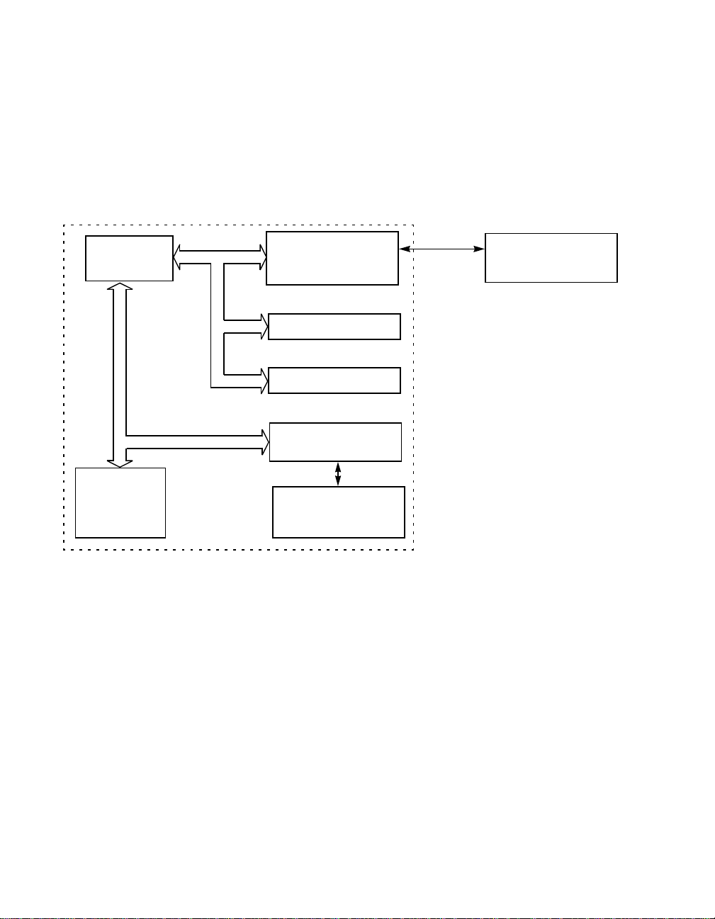
Figure 2.1 illustrates the relationship between these modules.
LSI53C895A PCI to Ultra2 SCSI Controller 2-1
Page 28
Figure 2 .1 LSI53C895A Block Diagram
PCI Bus
32-Bit PCI Interface, PCI Configuration Register
Wide Ultra2 SCSI Controller
8Kbyte
SCRIPTS RAM
8 Dword SCRIPTS
Prefetch Buffer
944 byte
DMA FIFO
SCSI FIFO and S C SI Control Block
JTAG
JTAG Bus Wide Ultra2 S CSI
Processor
SCSI SCRIPTS
Universal TolerANT
Drivers and Receivers
Bus
Operating
2.1 PCI Functional Description
The LSI53C895A implements a PCI-to-Wide Ultra2 SCSI controller.
2.1.1 PCI Addressing
There are three physical PCI-defined address spaces:
• PCI Configuration space.
Registers
ROM/Flash Memory Control
Local
Memory
Bus
ROM/Flash
Memory
Bus
and Autoconfiguration
Serial EEPROM Controller
2-Wire Serial
EEPROM
Bus
• I/O space for operating registers.
• Memory space for operating registers.
2-2 Functional Description
Page 29

2.1.1.1 Configuration Space
The host processor uses the PCI configuration space to initialize the
LSI53C895A through a defined set of configuration space registers. The
Configuration registers are accessible only by system BIOS during PCI
configuration cycles. The configuration space is a contiguous
256 X 8-bit set of addresses. Decoding C_BE[3:0]/ determines if a PCI
cycle is intended to access the configuration register space. The IDSEL
bus signal is a “chip select” that allows access to the configuration
register space only. A configuration read/write cycle without IDSEL is
ignored. The eight lower order address bits, AD[7:0], select a specific
8-bit register. AD[10:8] are decoded as well, but they must be zero or the
LSI53C895A does not respond. According to the PCI specification,
AD[10:8] are reserved for multifunction devices.
At initialization time, each PCI device is assigned a base address for I/O
and memory accesses. In the case of the LSI53C895A, the upper 24 bits
of the address are selected. On every access, the LSI53C895A
compares its assigned base addresses with the value on the
Address/Data bus during the PCI address phase. If the upper 24 bits
match, the access is for the LSI53C895A and the low-order eight bits
define the register being accessed. A decode of C_BE[3:0]/ determines
which registers and what type of access is to be performed.
2.1.1.2 I/O Space
The PCI specification defines I/O space as a contiguous
32-bit I/O address that is shared by all system resources, including the
LSI53C895A. Base Address Register Zero (I/O) determines which
256-byte I/O area this device occupies.
2.1.1.3 Memory Space
The PCI specification defines memory space as a contiguous 64-bit
memory address that is shared by all system resources, including the
LSI53C895A. Base Address Register One (MEMORY) determines which
1 Kbyte memory area this device occupies. Base Address Register Two
(SCRIPTS RAM) determines the 8 Kbyte memory area occupied by
SCRIPTS RAM.
PCI Functional Description 2-3
Page 30

2.1.2 PCI Bus Commands and Functions Supported
Bus commands indicate to the target the type of transaction the master
is requesting. Bus commands are encoded on the C_BE[3:0]/ lines
during the address phase. PCI bus commands and encoding types
appear in Table 2.1.
Table 2.1 PCI Bus Commands and Encoding Types for the LSI53C895A
C_BE[3:0]/ Command Type Supported as Master Supported as Slave
0b0000 Interrupt Acknowledge No No
0b0001 Special Cycle No No
0b0010 I/O Read Yes Yes
0b0011 I/O Write Yes Yes
0b0100 Reser ved n/a n/a
0b0101 Reser ved n/a n/a
0b0110 Memory Read Yes Yes
0b0111 Memory Write Yes Yes
0b1000 Reser ved n/a n/a
0b1001 Reser ved n/a n/a
0b1010 Configuration Read No Yes
0b1011 Configuration Write No Yes
0b1100 Memory Read Multiple Yes
0b1101 Dual Address Cycle (DAC) Yes No
0b1110 Memory Read Line Yes
0b1111 Memory Write and Invalidate Yes
1. See the DMA Mode (DMODE) register.
2. See the Chip Test Three (CTEST3) register.
1
1
2
2.1.2.1 Interrupt Acknowledge Command
The LSI53C895A does not respond to this command as a slave and it
never generates this command as a master.
2-4 Functional Description
Yes (defaults to 0b0110)
Yes (defaults to 0b0110)
Yes (defaults to 0b0111)
Page 31

2.1.2.2 Special Cycle Command
The LSI53C895A does not respond to this command as a slave and it
never generates this command as a master.
2.1.2.3 I/O Read Command
The I/O Read command reads data from an agent mapped in I/O
address space. All 32 address bits are decoded.
2.1.2.4 I/O Write Command
The I/O Write command writes data to an agent mapped in I/O address
space. All 32 address bits are decoded.
2.1.2.5 Reserved Command
The LSI53C895A does not respond to this command as a slave and it
never generates this command as a master.
2.1.2.6 Memory Read Command
The Memory Read command reads data from an agent mapped in the
Memory Address Space. The target is free to do an anticipatory read for
this command only if it can guarantee that such a read has no side
effects.
2.1.2.7 Memory Write Command
The Memory Write command writes data to an agent mapped in the
Memory Address Space. When the target returns “ready,” it assumes
responsibility for the coherency (which includes ordering) of the subject
data.
2.1.2.8 Configuration Read Command
The Configuration Read command reads the configuration space of each
agent. An agent is selected during a configuration access when its
IDSEL signal is asserted and AD[1:0] are 0b00.
PCI Functional Description 2-5
Page 32

2.1.2.9 Configuration Write Command
The Configuration Write command transfers data to the configuration
space of each agent. An agent is selected when its IDSEL signal is
asserted and AD[1:0] are 0b00.
2.1.2.10 Memory Read Multiple Command
This command is identical to the Memory Read command except that it
additionally indicates that the master may intend to fetch more than one
cache line before disconnecting. The LSI53C895A supports PCI Memory
Read Multiple functionality and issues Memory Read Multiple commands
on the PCI bus when the Read Multiple Mode is enabled. This mode is
enabled by setting bit 2 (ERMP) of the DMA Mode (DMODE) register. If
cache mode is enabled, a Memory Read Multiple command is issued on
all read cycles, except opcode fetches, when the following conditions are
met:
• The CLSE bit (Cache Line Size Enable, bit 7, DMA Control (DCNTL)
register) and the ERMP bit (Enable Read Multiple, bit 2, DMA Mode
(DMODE) register) are set.
• The CacheLineSizeregister for each function contains a legal burst
size value (2, 4, 8, 16, 32, or 64) and that value is less than or equal
to the DMODE burst size.
• The transfer will cross a cache line boundary.
When these conditions are met, the chip issues a Memory Read Multiple
command instead of a Memory Read during all PCI read cycles.
Burst Size Selection – The Read Multiple command reads in multiple
cache lines of data in a single bus ownership. The number of cache lines
to read is a multiple of the cache line size specified in Revision 2.2 of
the PCI specification. The logic selects the largest multiple of the cache
line size based on the amount of data to transfer, with the maximum
allowable burst size determined from the DMA Mode (DMODE) burst size
bits, and the Chip Test Five (CTEST5),bit2.
2-6 Functional Description
Page 33

2.1.2.11 Dual Address Cycle (DAC) Command
The LSI53C895A performs DACs when 64-bit addressing is required.
Refer to the PCI 2.2 specification. If any of the selector registers contain
a nonzero value, a DAC is generated. See 64-bit SCRIPTS Selectors in
Chapter 4, “Registers,” for additional information.
2.1.2.12 Memory Read Line Command
This command is identical to the Memory Read command, except that it
additionally indicates that the master intends to fetch a complete cache
line. This command is intended for use with bulk sequential data transfers
where the memory system and the requesting master might gain some
performance advantage by reading to a cache line boundary rather than
a single memory cycle. The Read Line function in the LSI53C895A takes
advantage of the PCI 2.2 specification regarding issuing this command.
If the cache mode is disabled, Read Line commands are not issued.
If the cache mode is enabled, a Read Line command is issued on all
read cycles, except nonprefetch opcode fetches, when the following
conditions are met:
• The CLSE (Cache Line Size Enable, bit 7, DMA Control (DCNTL)
register) and ERL (Enable Read Line, bit 3, DMA Mode (DMODE)
register) bits are set.
• The Cache Line Size register must contain a legal burst size value
in Dwords (2, 4, 8, 16, 32, 64, or 128) and that value is less than or
equal to the DMA Mode (DMODE) burst size.
• The transfer will cross a Dword boundary but not a cache line
boundary.
When these conditions are met, the chip issues a Read Line command
instead of a Memory Read during all PCI read cycles. Otherwise, it
issues a normal Memory Read command.
Read Multiple with Read Line Enabled – When both the Read
Multiple and Read Line modes are enabled, the Read Line command is
not issued if the above conditions are met. Instead, a Read Multiple
command is issued, even though the conditions for Read Line are met.
PCI Functional Description 2-7
Page 34

If the Read Multiple mode is enabled and the Read Line mode is
disabled, Read Multiple commands are issued if the Read Multiple
conditions are met.
2.1.2.13 Memory Write and Invalidate Command
The Memory Write and Invalidate command is identical to the Memory
Write command, except that it additionally guarantees a minimum
transfer of one complete cache line; that is to say, the master intends to
write all bytes within the addressed cache line in a single PCI transaction
unless interrupted by the target. This command requires implementation
of the PCI Cache Line Size register at address 0x0C in PCI configuration
space. The LSI53C895A enables Memory Write and Invalidate cycles
when bit 0 (WRIE) in the Chip Test Three (CTEST3) register and bit 4
(WIE) in the PCI Command register are set. When the following
conditions are met, Memory Write and Invalidate commands are issued:
1. The CLSE bit (Cache Line Size Enable, bit 7, DMA Control (DCNTL)
register), WRIE bit (Write and Invalidate Enable, bit 0, Chip Test
Three (CTEST3) register), and PCI configuration Command register,
bit 4 are set.
2. The Cache Line Size register contains a legal burst size value in
Dwords (2, 4, 8, 16, 32, 64, or 128) and that value is less than or
equal to the DMA Mode (DMODE) burst size.
3. The chip has enough bytes in the DMA FIFO to complete at least
one full cache line burst.
4. The chip is aligned to a cache line boundary.
When these conditions are met, the LSI53C895A issues a Memory Write
and Invalidate command instead of a Memory Write command during all
PCI write cycles.
Multiple Cache Line Transfers – The Memory Write and Invalidate
command can write multiple cache lines of data in a single bus
ownership. The chip issues a burst transfer as soon as it reaches a
cache line boundary. The size of the transfer is not automatically the
cache line size, but rather a multiple of the cache line size specified in
Revision 2.2 of the PCI specification. The logic selects the largest
multiple of the cache line size based on the amount of data to transfer,
with the maximum allowable burst size determined from the DMA Mode
2-8 Functional Description
Page 35

(DMODE) burst size bits, and Chip Test Five (CTEST5), bit2.Ifmultiple
cache line size transfers are not desired, set the DMA Mode (DMODE)
burst size to exactly the cache line size and the chip only issues single
cache line transfers.
After each data transfer, the chip re-evaluates the burst size based on
the amount of remaining data to transfer and again selects the highest
possible multiple of the cache line size, and no larger than the DMA
Mode (DMODE) burst size. The most likely scenario of this scheme is
that the chip selects the DMA Mode (DMODE) burst size after alignment,
and issues bursts of this size. The burst size is, in effect, throttled down
toward the end of a long Memory Move or Block Move transfer until only
the cache line size burst size is left. The chip finishes the transfer with
this burst size.
Latency – In accordance with the PCI specification, the latency timer is
ignored when issuing a Memory Write and Invalidate command such that
when a latency time-out occurs, the LSI53C895A continues to transfer
up to a cache line boundary. At that point, the chip relinquishes the bus,
and finishes the transfer at a later time using another bus ownership. If
the chip is transferring multiple cache lines it continues to transfer until
the next cache boundary is reached.
PCI Target Retry – During a Memory Write and Invalidate transfer, if the
target deviceissues a retry (STOP with no TRDY/, indicating that no data
was transferred), the chip relinquishes the bus and immediately tries to
finish the transfer on another bus ownership. The chip issues another
Memory Write and Invalidate command on the next ownership, in
accordance with the PCI specification.
PCI Target Disconnect – During a Memory Write and Invalidate
transfer, if the target device issues a disconnect the LSI53C895A
relinquishes the bus and immediately tries to finish the transfer on
another bus ownership. The chip does not issue another Memory Write
and Invalidate command on the next ownership unless the address is
aligned.
2.1.3 PCI Cache Mode
The LSI53C895A supports the PCI specification for an 8-bit Cache Line
Size register located in the PCI configuration space. The Cache Line
Size register provides the ability to sense and react to nonaligned
PCI Functional Description 2-9
Page 36

addresses corresponding to cache line boundaries. In conjunction with
the CacheLineSizeregister, the PCI commands Memory Read Line,
Memory Read Multiple, Memory Write and Invalidate are each software
enabled or disabled to allow the user full flexibility in using these
commands.
2.1.3.1 Enabling Cache Mode
In order to enable the cache logic to issue PCI cache commands
(Memory Read Line, Memory Read Multiple, and Memory Write and
Invalidate) on any given PCI master operation the following conditions
must be met:
• The Cache Line Size Enable bit in DMA Control (DCNTL) register
must be set.
• The PCI CacheLineSizeregister must contain a valid binary cache
size, i.e. 2, 4, 8, 16, 32, 64, or 128 Dwords. Only these values are
considered valid cache sizes.
• The programmed burst size (in Dwords) must be equal to or greater
than the CacheLineSizeregister. The DMA Mode (DMODE) register
bits [7:6] and Chip Test Five (CTEST5) bit 2 are the burst length bits.
• The part must be doing a PCI Master transfer. The following PCI
Master transactions do not utilize the PCI cache logic and thus no
PCI cache command is issued during these types of cycles: a
nonprefetch SCRIPTS fetch, a Load/Store data transfer, a data flush
operation. All other types of PCI Master transactions will utilize the
PCI cache logic.
The above four conditions must be met for the cache logic to control the
type of PCI cache command that is issued, along with any alignment that
may be necessary during write operations. If these conditions are not
met for any given PCI Master transaction, a Memory Read or Memory
Write is issued and no cache write alignment is done.
2.1.3.2 Issuing Cache Commands
In order to issue each type of PCI cache command, the corresponding
enable bit must be set (2 bits in the case of Memory Write and
Invalidate). These bits are detailed below:
2-10 Functional Description
Page 37

• To issue Memory Read Line commands, the Read Line enable bit in
the DMA Mode (DMODE) register must be set.
• To issue Memory Read Multiple commands, the Read Multiple
enable bit in the DMA Mode (DMODE) register must be set.
• To issue Memory Write and Invalidate commands, both the Write and
Invalidate enables in the Chip Test Three (CTEST3) register and the
PCI configuration command register must be set.
If the corresponding cache command being issued is not enabled then
the cache logic falls back to the next command enabled. Specifically, if
Memory Read Multiple is not enabled and Memory Read Lines are, read
lines are issued in place of read multiple. If no cache commands are
enabled, cache write alignment still occurs but no cache commands are
issued, only memory reads and memory writes.
2.1.3.3 Memory Read Caching
The type of Memory Read command issued depends on the starting
location of the transfer and the number of bytes being transferred. During
reads, no cache alignment is done (this is not required nor optimal per
PCI 2.2 specification) and reads will always be either a programmed
burst length in size, as set in the DMA Mode (DMODE) and Chip Test
Three (CTEST3) registers. In the case of a transfer which is smaller than
the burst length, all bytes for that transfer are read in one PCI burst
transaction. If the transfer will cross a Dword boundary (A[1:0] = 0b00) a
Memory Read Line command is issued. When the transfer will cross a
cache boundary (depends on cache line size programmed into the PCI
configuration register), a Memory Read Multiple command is issued. If a
transfer will not cross a Dword or cache boundary or if cache mode is
not enabled a Memory Read command is issued.
2.1.3.4 Memory Write Caching
Writes are aligned in a single burst transfer to get to a cache boundary.
At that point, Memory Write and Invalidate commands are issued and
continue at the burst length programmed into the DMA Mode (DMODE)
register. Memory Write and Invalidate commands are issued as long as
the remaining byte count is greater than the Memory Write and Invalidate
threshold. When the byte count goes below this threshold, a single
Memory Write burst is issued to complete the transfer. The general
pattern for PCI writes is:
PCI Functional Description 2-11
Page 38

• A single Memory Write to align to a cache boundary.
• Multiple Memory Write and Invalidates.
• A single data residual Memory Write to complete the transfer.
Table 2.2 describes PCI cache mode alignment.
2-12 Functional Description
Page 39

Table 2.2 PC I Cache Mode Alignment
Host Memory
A0x00
B0x04
0x08
C0x0C
D0x10
0x14
0x18
0x1C
E0x20
0x24
0x28
0x2C
F0x30
0x34
0x38
0x3C
G0x40
0x44
0x48
0x4C
H0x50
0x54
0x58
0x5C
0x60
PCI Functional Description 2-13
Page 40

2.1.3.5 Examples:
The examples in this section employ the following abbreviations:
MR = Memory Read, MRL = Memory Read Line, MRM = Memory Read
Multiple, MW = Memory Write, MWI = Memory Write and Invalidate.
Read Example 1 –
Burst=4Dwords,CacheLineSize=4Dwords:
AtoB: MRL(6bytes)
AtoC: MRL (13 bytes)
AtoD: MRL (15 bytes)
MR (2 bytes)
CtoD: MRM (5 bytes)
CtoE: MRM (15 bytes)
MRM (6 bytes)
DtoF: MRL (15 bytes)
AtoH: MRL (15 bytes)
AtoG: MRL (15 bytes)
MRL (16 bytes)
MR (1 byte)
MRL (16 bytes)
MRL (16 bytes)
MRL (16 bytes)
MRL (16 bytes)
MR (2 bytes)
MRL (16 bytes)
MRL (16 bytes)
MRL (16 bytes)
MR (3 bytes)
2-14 Functional Description
Page 41

Read Example 2 –
Burst=8Dwords,CacheLineSize=4Dwords:
AtoB: MRL(6bytes)
AtoC: MRL (13 bytes)
AtoD: MRM (17 bytes)
CtoD: MRM (5 bytes)
CtoE: MRM (21 bytes)
DtoF: MRM (31 bytes)
MR (1 byte)
AtoH: MRM (31 bytes)
AtoG: MRM (31 bytes)
MRM (32 bytes)
MRM (18 bytes)
MRM (32 bytes)
MR (3 bytes)
Read Example 3 –
Burst = 16 Dwords, Cache Line Size = 8 Dwords:
AtoB: MRL(6bytes)
AtoC: MRL (13 bytes)
AtoD: MRL (17 bytes)
CtoD: MRL(5bytes)
CtoE: MRM (21 bytes)
DtoF: MRM (32 bytes)
AtoH: MRM (63 bytes)
MRL (16 bytes)
MRM (2 bytes)
AtoG: 2 transfers, MRM (63 bytes), MR (3 bytes)
PCI Functional Description 2-15
Page 42

Write Example 1 –
Burst=4Dwords,CacheLineSize=4Dwords:
AtoB: MW (6 bytes)
AtoC: MW (13 bytes)
AtoD: MW (17 bytes)
CtoD: MW (5 bytes)
CtoE: MW (3 bytes)
DtoF: MW (15 bytes)
AtoH: MW (15 bytes)
AtoG: MW (15 bytes)
MWI (16 bytes)
MW (2 bytes)
MWI (16 bytes)
MW (1 byte)
MWI (16 bytes)
MWI (16 bytes)
MWI (16 bytes)
MWI (16 bytes)
MW (2 bytes)
MWI (16 bytes)
MWI (16 bytes)
MWI (16 bytes)
MW (3 bytes)
2-16 Functional Description
Page 43

Write Example 2 –
Burst=8Dwords,CacheLineSize=4Dwords:
AtoB: MW (6 bytes)
AtoC: MW (13 bytes)
AtoD: MW (17 bytes)
CtoD: MW (5 bytes)
CtoE: MW (3 bytes)
DtoF: MW (15 bytes)
AtoH: MW (15 bytes)
AtoG: MW (15 bytes)
MWI (16 bytes)
MW (2 bytes)
MWI (16 bytes)
MW (1 byte)
MWI (32 bytes)
MWI (32 bytes)
MW (2 bytes)
MWI (32 bytes)
MWI (16 bytes)
MW (3 bytes)
PCI Functional Description 2-17
Page 44

Write Example 3 –
Burst = 16 Dwords, Cache Line Size = 8 Dwords:
AtoB: MW (6 bytes)
AtoC: MW (13 bytes)
AtoD: MW (17 bytes)
CtoD: MW (5 bytes)
CtoE: MW (21 bytes)
DtoF: MW (32 bytes)
AtoH: MW (15 bytes)
AtoG: MW (15 bytes)
MWI (64 bytes)
MW (2 bytes)
MWI (32 bytes)
MW (18 bytes)
2.1.3.6 Memory-to-Memory Moves
Memory-to-Memory Moves also support PCI cache commands, as
described above, with one limitation. Memory Write and Invalidate on
Memory-to-Memory Move writes are only supported if the source and
destination address are quad word aligned. If the source and destination
are not quad word aligned (that is, Source address [2:0] == Destination
Address [2:0]), write aligning is not performed and Memory Write and
Invalidate commands are not issued. The LSI53C895A is little endian
only.
2.2 SCSI Functional Description
The LSI53C895A provides an Ultra2 SCSI controller that supports an
8-bit or 16-bit bus. The controller supports Wide Ultra2 SCSI
synchronous transfer rates up to 80 Mbytes/s on a LVD SCSI bus. The
SCSIcorecanbeprogrammedwithSCSISCRIPTS,makingiteasyto
“fine tune” the system for specific mass storage devices or Ultra2 SCSI
requirements.
2-18 Functional Description
Page 45

The LSI53C895A offers low level register access or a high-level control
interface. Like first generation SCSI devices, the LSI53C895A is
accessed as a register-oriented device. Error recovery and/or diagnostic
procedures use the ability to sample and/or assert any signal on the
SCSI bus. In support of SCSI loopback diagnostics, the SCSI core may
perform a self-selection and operate as both an initiator and a target.
The LSI53C895A is controlled by the integrated SCRIPTS processor
through a high-level logical interface. Commands controlling the SCSI
core are fetched out of the main host memory or local memory. These
commands instruct the SCSI core to Select, Reselect, Disconnect, Wait
for a Disconnect, Transfer Information, Change Bus Phases and, in
general, implement all aspects of the SCSI protocol. The SCRIPTS
processor is a special high-speed processor optimized for SCSI protocol.
2.2.1 SCRIPTS Processor
The SCSI SCRIPTS processor allows both DMA and SCSI commands
to be fetched from host memory or internal SCRIPTS RAM. Algorithms
written in SCSI SCRIPTS control the actions of the SCSI and DMA
cores. The SCRIPTS processor executes complex SCSI bus sequences
independently of the host
Algorithms may be designed to tune SCSI bus performance, to adjust to
new bus device types (such as scanners, communication gateways, etc.),
or to incorporate changes in the SCSI-2 or SCSI-3 logical bus definitions
without sacrificing I/O performance. SCSI SCRIPTS are hardware
independent, so they can be used interchangeably on any host or CPU
system bus. SCSI SCRIPTS handle conditions like Phase Mismatch.
= CPU.
2.2.1.1 Phase Mismatch Handling in SCRIPTS
The LSI53C895A can handle phase mismatches due to drive
disconnects without needing to interrupt the processor. The primary goal
of this logic is to completely eliminate the need for CPU intervention
during an I/O disconnect/reselect sequence.
Storing the appropriate information to later restart the I/O can be done
through SCRIPTS, eliminating the need for processor intervention during
an I/O disconnect/reselect sequence. Calculations are performed such
that the appropriate information is av ailable to SCRIPTS so that an I/O
state can be properly stored for restart later.
SCSI Functional Description 2-19
Page 46

The Phase Mismatch Jump logic powers up disabled and must be
enabled by setting the Phase Mismatch Jump Enable bit (ENPMJ, bit 7
in the Chip Control 0 (CCNTL0) register).
Utilizing the information supplied in the PhaseMismatchJumpAddress
1(PMJAD1)and Phase Mismatch Jump Address 2 (PMJAD2) registers,
described in Chapter 4, “Registers,” SCRIPTS handles all overhead
involved in a disconnect/reselect sequence with a modest number of
instructions.
2.2.2 Internal SCRIPTS RAM
The LSI53C895A has 8 Kbyte (2048 x 32 bits) of internal, general
purpose RAM. The RAM is designed for SCRIPTS program storage, but
is not limited to this type of information. When the chip fetches SCRIPTS
instructions or Table Indirect information from the internal RAM, these
fetches remain internal to the chip and do not use the PCI bus. Other
types of access to the RAM by the chip, except Load/Store, use the PCI
bus, as if they were external accesses. The SCRIPTS RAM
powers up enabled by default.
The RAM can be relocated by the PCI system BIOS anywhere in the
32-bit address space. The Base Address Register Two (SCRIPTS RAM)
in the PCI configuration space contains the base address of the internal
RAM. To simplify loading of the SCRIPTS instructions, the base address
of the RAM appears in the Scratch Register B (SCRATCHB) register
when bit 3 of the Chip Test Two (CTEST2) register is set. The RAM is
byte accessible from the PCI bus and is visible to any bus mastering
device on the bus. External accesses to the RAM (by the CPU) follow
the same timing sequence as a standard slave register access, except
that the required target wait-states drop from 5 to 3.
A complete set of development tools is available for writing custom
drivers with SCSI SCRIPTS. For more information on the SCSI SCRIPTS
instructions supported by the LSI53C895A, see Chapter 5, “SCSI
SCRIPTS Instruction Set.”
2-20 Functional Description
Page 47

2.2.3 64-Bit Addressing in SCRIPTS
The LSI53C895A has a 32-bit PCI interface which provides 64-bit
address capability in the initiator mode.
DACs can be generated for all SCRIPTS operations. There are six
selector registers which hold the upper Dword of a 64-bit address. All but
one of these is static and requires manual loading using a CPU access,
a Load/Store instruction, or a Memory Mov e instruction. One of the
selector registers is dynamic and is used during 64-bit direct block moves
only. All selectors default to zero, meaning the LSI53C895A powers-up
in a state where only Single Address Cycles (SACs) are generated.
When any of the selector registers are written to a nonzero value, DACs
are generated.
Direct, Table Indirect and Indirect Block moves, Memory-to-Memory
Moves, Load and Store instructions, and jumps are all instructions with
64-bit address capability.
Crossing the 4 Gbyte boundary on any one SCRIPTS operation is not
permitted and software needs to take care that any given SCRIPTS
operation will not cross the 4 Gbyte boundary.
2.2.4 Hardware Control of SCSI Activity LED
The LSI53C895A has the ability to control a LED through the GPIO_0
pin to indicate that it is connected to the SCSI bus. Formerly this function
was done by a software driver.
When bit 5 (LED_CNTL) in the General Purpose Pin Control Zero
(GPCNTL0) register is set and bit 6 (Fetch Enable) in the General
Purpose Pin Control Zero (GPCNTL0) register is cleared and the
LSI53C895A is not performing an EEPROM autodownload, then bit 3
(CON) in the Interrupt Status Zero (ISTAT0) register is presented at the
GPIO_0 pin.
The CON (Connected) bit in Interrupt Status Zero (ISTAT0) is set anytime
the LSI53C895A is connected to the SCSI bus either as an initiator or a
target. This will happen after the LSI53C895A has successfully
completed a selection or when it has successfully responded to a
selection or reselection. It will also be set when the LSI53C895A wins
arbitration in low level mode.
SCSI Functional Description 2-21
Page 48

2.2.5 Designing an Ultra2 SCSI System
Since Ultra2 SCSI is based on existing SCSI standards, it can use
existing driver programs as long as the software is able to negotiate for
Ultra2 SCSI synchronous transfer rates. Additional software
modifications are needed to take advantage of the new features in the
LSI53C895A.
In the area of hardware, LVD SCSI is required to achieve Ultra2 SCSI
transfer rates and to support the longer cable and additional devices on
the bus. All devices on the bus must have LVD SCSI capabilities to
guarantee Ultra2 SCSI transfer rates.For additional information on Ultra2
SCSI, refer to the SPI-2 working document which is available from the
SCSI BBS referenced at the beginning of this manual.
Chapter 6, “Electrical Specifications,” contains Ultra2 SCSI timing
information. In addition to the guidelines in the draft standard, make the
following software and hardware adjustments to accommodate Ultra2
SCSI transfers:
• Set the Ultra Enable bit to enable Ultra2 SCSI transfers.
• Set the TolerANT Enable bit, bit 7 in the SCSI Test Three (STEST3)
register, whenever the Ultra Enable bit is set.
• Do not extend the SREQ/SACK filtering period with SCSI Test Two
(STEST2) bit 1. When the Ultra Enable bit is set, the filtering period
isfixedat8nsforUltra2SCSIor15nsforUltraSCSI,regardlessof
the value of the SREQ/SACK Filtering bit.
• Use the SCSI clock quadrupler.
A 40 MHz input must be supplied if using the SCSI clock quadrupler
for an Ultra2 design.
2.2.5.1 Using the SCSI Clock Quadrupler
The LSI53C895A can quadruple the frequency of a 40 MHz SCSI clock,
allowing the system to perform Ultra2 SCSI transfers. This option is user
selectable with bit settings in the SCSI Test One (STEST1), SCSI Te st
Three (STEST3),andSCSI Control Three (SCNTL3) registers. At
power-on or reset, the quadrupler is disabled and powered down. Follow
these steps to use the clock quadrupler:
2-22 Functional Description
Page 49

Step 1. Set the SCLK Quadrupler Enable bit (SCSI Test One
(STEST1),bit3).
Step 2. Poll bit 5 of the SCSI Test Four (STEST4) register. The
LSI53C895A sets this bit as soon as it locks in the 160 MHz
frequency. The frequency lockup takes approximately
100 microseconds.
Step3. HalttheSCSIclockbysettingtheHaltSCSIClockbit(SCSI
Test Three (STEST3),bit5).
Step 4. Set the clock conversion factor using the SCF and CCF fields
in the SCSI Control Three (SCNTL3) register.
Step 5. Set the SCLK Quadrupler Select bit (SCSI Test One (STEST1),
bit 2).
Step 6. Clear the Halt SCSI Clock bit.
2.2.6 Prefetching SCRIPTS Instructions
When enabled by setting the Prefetch Enable bit (bit 5) in the DMA
Control (DCNTL) register, the prefetch logic in the LSI53C895A fetches
8 Dwords of instructions. The prefetch logic automatically determines the
maximum burst size that it can perform, based on the burst length as
determined by the values in the DMA Mode (DMODE) register. If the unit
cannot perform bursts of at least four Dwords, it disables itself. While the
chip is prefetching SCRIPTS instructions, it will use PCI cache
commands Memory Read Line, and Memory Read Multiple, if PCI
caching is enabled.
Note:
The LSI53C895A may flush the contents of the prefetch unit under
certain conditions, listed below, to ensure that the chip always operates
from the most current version of the SCRIPTS instruction. When one of
these conditions apply, the contents of the prefetch unit are automatically
flushed.
This feature is only useful if fetching SCRIPTS instructions
from main memory. Due to the short access time of
SCRIPTS RAM, prefetching is not necessary when fetching
instructions from this memory.
• On every Memory Move instruction. The Memory Move instruction is
often used to place modified code directly into memory. To make
sure that the chip executes all recent modifications, the prefetch unit
SCSI Functional Description 2-23
Page 50

flushes its contents and loads the modified code every time an
instruction is issued. To avoid inadvertently flushing the prefetch unit
contents, use the No Flush option for all Memory Move operations
that do not modify code within the ne xt 8 Dwords. For more
information on this instruction refer to Chapter 5, “SCSI SCRIPTS
Instruction Set.”
• On every Store instruction. The Store instruction may also be used
to place modified code directly into memory. To avoid inadvertently
flushing the prefetch unit contents use the No Flush option for all
Store operations that do not modify code within the next 8 Dwords.
• On every write to the DMA SCRIPTS Pointer (DSP) register.
• On all Transfer Control instructions when the transfer conditions are
met. This is necessary because the next instruction to execute is not
the sequential next instruction in the prefetch unit.
• WhenthePrefetchFlushbit(DMA Control (DCNTL) register, bit 6)
is set. The unit flushes whenever this bit is set. The bit is
self-clearing.
2.2.7 Opcode Fetch Burst Capability
Setting the Burst Opcode Fetch Enable bit (bit 1) in the DMA Mode
(DMODE) register (0x38) causes the LSI53C895A to burst in the first two
Dwords of all instruction fetches. If the instruction is a Memory-toMemory Move, the third Dword is accessed in a separate ownership. If
the instruction is an indirect type, the additional Dword is accessed in a
subsequent bus ownership. If the instruction is a Tabl e Indirect Block
Move, the chip uses two accesses to obtain the four Dwords required, in
two bursts of two Dwords each.
Note:
This feature is only useful if Prefetching is disabled and
SCRIPTS instructions are fetched from main memory. Due
to the short SCRIPTS RAM access time, burst opcode
fetching is not necessary when fetching instructions from
this memory.
2.2.8 Load and Store Instructions
The LSI53C895A supports the Load and Store instruction type, which
simplifies the movement of data between memory and the internal chip
registers. It also enables the chip to transfer bytes to addresses relative
2-24 Functional Description
Page 51

to the Data Structure Address (DSA) register. Load and Store data
transfers to or from the SCRIPTS RAM will remain internal to the chip
and will not generate PCI bus cycles. While a Load/Store to or from
SCRIPTS RAM is occurring, any external PCI slave cycles that occur are
retried on the PCI bus. This feature can be disabled by setting the DILS
bit in the Chip C ontrol 0 (CCNTL0) register. For more information on the
Load and Store instructions, refer to Chapter 5, “SCSI SCRIPTS
Instruction Set.”
2.2.9 JTAG Boundary Scan Testing
The LSI53C895A includes support for JTAG boundary scan testing in
accordance with the IEEE 1149.1 specification with one exception, which
is explained in this section. This device accepts all required boundary
scan instructions including the optional CLAMP, HIGH-Z, and IDCODE
instructions.
The LSI53C895A uses an 8-bit instruction register to support all
boundary scan instructions. The data registers included in the device are
the Boundary Data register, the IDCODE register, and the Bypass
register. This device can handle a 10 MHz TCK frequency for TDO and
TDI.
Due to design constraints, the RST/ pin (system reset) always 3-states
the SCSI pins when it is asserted. Boundary scan logic does not control
this action, and this is not compliant with the specification. There are two
solutions that resolve this issue:
1. Use the RST/ pin as a boundary scan compliance pin. When the pin
is deasserted, the device is boundary scan compliant and when
asserted, the device is noncompliant. To maintain compliance the
RST/pinmustbedrivenHIGH.
2. When RST/ is asserted during boundary scan testing the expected
output on the SCSI pins must be the HIGH-Z condition, and not what
is contained in the boundary scan data registers for the SCSI pin
output cells.
SCSI Functional Description 2-25
Page 52

2.2.10 SCSI Loopback Mode
The LSI53C895A loopback mode allows testing of both initiator and
target functions and, in effect, lets the chip communicate with itself.
When the Loopback Enable bit is set in the SCSI Test Two (STEST2)
register, bit 4, the LSI53C895A allows control of all SCSI signals whether
the chip is operating in the initiator or target mode. For more information
on this mode of operation refer to the LSI Logic SCSI SCRIPTS
Processors Programming Guide.
2.2.11 Parity Options
The LSI53C895A implements a flexible parity scheme that allows control
of the parity sense, allows parity checking to be turned on or off, and has
the ability to deliberately send a byte with bad parity over the SCSI bus
to test parity error recovery procedures. Table 2.3 defines the bits that
are involved in parity control and observation. Table 2.4 describes the
parity control function of the Enable Parity Checking and Assert SCSI
Even Parity bits in the SCSI Control One (SCNTL1) register, bit 2.
Table 2.5 describes the options available when a parity error occurs.
Figure 2.2 shows where parity checking is done in the LSI53C895A.
2-26 Functional Description
Page 53

Table 2.3 Bits Used for Parity Control and Generation
Bit Name Location Description
Assert SATN/ on
Parity Errors
Enable Parity
Checking
Assert Even SCSI
Parity
Disable Halt on
SATN/ or a Parity
Error (Target Mode
Only)
Enable Parity Error
Interrupt
Parity Error SCSI Interrupt
Status of SCSI
Parity Signal
SCSI SDP1 Signal SCSI Status Two
Latched SCSI Parity SSTAT 2, Bit 3 and
SCSI Control Zero
(SCNTL0),Bit1
SCSI Control Zero
(SCNTL0),Bit3
SCSI Control One
(SCNTL1),Bit2
SCSI Control One
(SCNTL1),Bit5
SCSI Interrupt
Enable Zero
(SIEN0),Bit0
Status Zero
(SIST0),Bit0
SCSI Status Zero
(SSTAT0),Bit0
(SSTAT2),Bit0
SCSI Status One
(SSTAT1),Bit3
Causes the LSI53C895A to automatically assert SATN/
when it detects a SCSI parity error while operating as an
initiator.
Enables the LSI53C895A to check for parity errors. The
LSI53C895A checks for odd parity.
Determines the SCSI parity sense generated by the
LSI53C895A to the SCSI bus.
Causes the LSI53C895A not to halt operations when a
parity error is detected in target mode.
Determines whether the LSI53C895A generates an
interrupt when it detects a SCSI parity error.
This status bit is set whenever the LSI53C895A detects a
parity error on the SCSI bus.
This status bit represents the active HIGH current state of
the SCSI SDP0 parity signal.
This bit represents the active HIGH current state of the
SCSI SDP1 parity signal.
These bits reflect the SCSI odd parity signal
corresponding to the data latched into the SCSI Input
Data Latch (SIDL) register.
Master Parity Error
Enable
Master Data Parity
Error
Master Data Parity
Error Interrupt
Enable
Chip Test Four
(CTEST4),Bit3
DMA Status
(DSTAT),Bit6
DMA Interrupt
Enable (DIEN),
Bit 6
SCSI Functional Description 2-27
Enables parity checking during PCI master data phases.
Set when the LSI53C895A
target device signaling a parity error during a data phase.
By clearing this bit, a Master Data Parity Error does not
cause assertion of INTA/ (or INTB/), but the status bit is
set in the DMA Status (DSTAT) register.
, as a PCI master, detects a
Page 54

Table 2.4 SCSI Parity Control
EPC
1
ASEP
2
Description
0 0 Does not check for parity errors. Parity is generated when sending
SCSI data. Asserts odd parity when sending SCSI data.
0 1 Does not check for parity errors. Parity is generated when sending
SCSI data. Asserts even parity when sending SCSI data.
1 0 Checks for odd parity on SCSI data received. Parity is generated when
sending SCSI data. Asserts odd parity when sending SCSI data.
1 1 Checks for odd parity on SCSI data received. Parity is generated when
sending SCSI data. Asserts even parity when sending SCSI data.
1. EPC = Enable Parity Checking (bit 3 SCSI Control Zero (SCNTL0)).
2. ASEP = Assert SCSI Even Parity (bit 2 SCSI Control One (SCNTL1)).
Table 2.5 SCSI Parity Errors and Interrupts
1
DHP
0 0 Halts when a parity error occurs in the target or initiator mode and does
0 1 Halts when a parity error occurs in the target mode and generates an
PAR
2
Description
NOT generate an interrupt.
interrupt in the target or initiator mode.
1 0 Does not halt in target mode when a parity error occurs until the end
of the transfer. An interrupt is not generated.
1 1 Does not halt in target mode when a parity error occurs until the end
of the transfer. An interrupt is generated.
1. DHP = Disable Halt on SATN/ or Parity Error (bit 5 SCSI Control One (SCNTL1)).
2. PAR = Parity Error (bit 0 SCSI Interrupt Enable Zero (SIEN0)).
2-28 Functional Description
Page 55
Figure 2.2 Parity Checking/Generation
Asynchronous
SCSI Send
PCI Interface**
X
DMA FIFO*
(64 bits X 118)
SODL Register*
S
SCSI Interface**
X = Check parity
G = Generate 32 bit even PCI parity
S = Generate 8 bit odd SCSI parity
Asynchronous
SCSI Receive
PCI Interface**
DMA FIFO*
(64 bits X 118)
SIDL Register*
SCSI Interface**
2.2.12 DMA FIFO
Synchronous
SCSI Send
PCI Interface**
G
(64 bits X 118)
SODL Register*
X
SODR Register* SCSI Interface**
SCSI Interface**
X
DMA FIFO*
S
*
**
Synchronous
SCSI Receive
PCI Interface**
G
DMA FIFO*
(64 bits X 118)
X
SCSI FIFO**
(8 or 16 bits x 31)
X
= No parity protection
= Parity protected
The DMA FIFO is 8 bytes wide by 118 transfers deep. The DMA FIFO is
illustrated in Figure 2.3. The default DMA FIFO size is 112 bytes to
assure compatibility with older products in the LSI53C8XX family.
The DMA FIFO size may be set to 944 bytes by setting the DMA FIFO
Size bit, bit 5, in the Chip Test Five (CTEST5) register.
SCSI Functional Description 2-29
Page 56
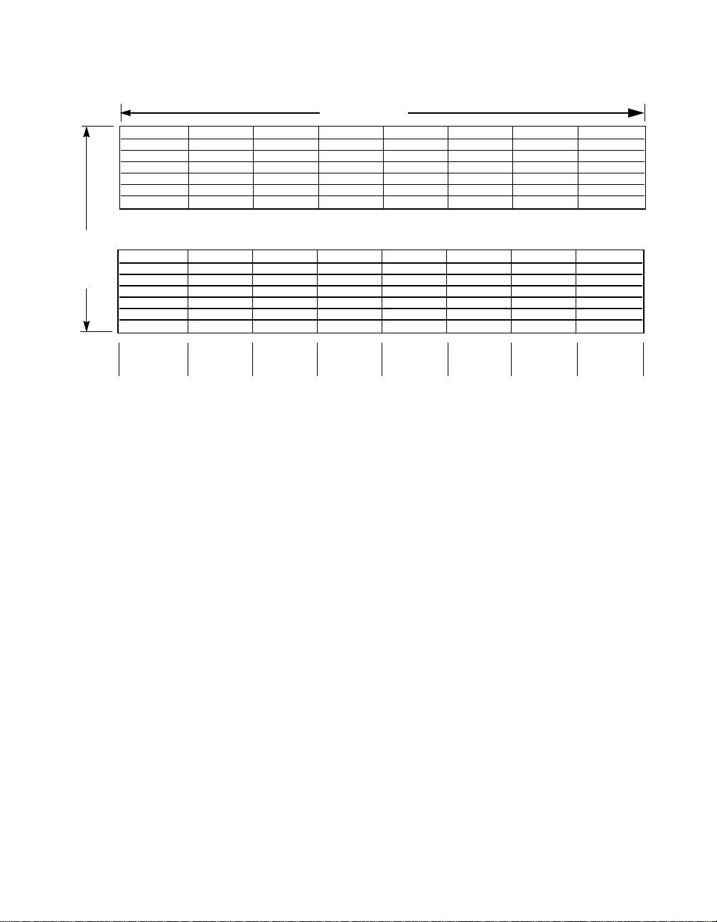
Figure 2.3 DMA FIFO Sections
8 Bytes Wide
.
.
.
118
Transfers
Deep
8Bits
Byte Lane 7
2.2.12.1 Data Paths
8Bits
Byte Lane 6
8Bits
Byte Lane 5
8Bits
Byte Lane 4
8Bits
Byte Lane 3
8Bits
Byte Lane 2
8Bits
Byte Lane 1
8Bits
Byte Lane 0
The LSI53C895A automatically supports misaligned DMA transfers. A
944-byte FIFO allows the LSI53C895A to support 2, 4, 8, 16, 32, 64, or
128 Dword bursts across the PCI bus interface.
The data path through the LSI53C895A is dependent on whether data is
being moved into or out of the chip, and whether SCSI data is being
transferred asynchronously or synchronously.
Figure 2.4 shows how data is moved to/from the SCSI bus in each of the
different modes.
.
.
.
2-30 Functional Description
Page 57
Figure 2.4 LSI53C895A Host Interface SCSI Data Paths
Asynchronous
SCSI Send
PCI Interface**
DMA FIFO*
(8 Bytes x 118)
SODL Register*
SCSI Interface**
Asynchronous
SCSI Receive
PCI Interface**
DMA FIFO*
(8 Bytes x 118)
SWIDE Register
SIDL Register*
SCSI Interface**
Synchronous
SCSI Send
PCI Interface**
DMA FIFO*
(8 Bytes x 118)
SODL Register*
SODR Register* SCSI Interface**
SCSI Interface**
Synchronous
SCSI Receive
PCI Interface**
DMA FIFO*
(8 Bytes x 118)
SCSI FIFO**
(1 or 2 Bytes x 31)
* = No parity protection
** = Parity protected
SWIDE Register
The following steps determine if any bytes remain in the data path when
the chip halts an operation:
Asynchronous SCSI Send –
Step 1. If the DMA FIFO size is set to 112 bytes (bit 5 of the Chip Test
Five (CTEST5) register cleared), look at the DMA FIFO
(DFIFO) and DMA Byte Counter (DBC) registers and calculate
if there are bytes left in the DMA FIFO. To make this calculation,
subtract the seven least significant bits of the DBC register from
the 7-bit value of the DFIFO register. AND the result with 0x7F
for a byte count between zero and 112.
If the DMA FIFO size is set to 944 bytes (bit 5 of the Chip Test
Five (CTEST5) register is set), subtract the 10 least significant
bits of the DBC register from the 10-bit value of the DMA FIFO
SCSI Functional Description 2-31
Page 58

Byte Offset Counter, which consists of bits [1:0] in the CTEST5
register and bits [7:0] of the DMA FIFO register. AND the result
with 0x3FF for a byte count between zero and 944.
Step 2. Read bit 5 in the SCSI Status Zero (SSTAT0) and SCSI Status
Two (SSTAT2) registers to determine if any bytes are left in the
SCSI Output Data Latch (SODL) register.Ifbit5issetinthe
SSTAT0 or SST AT2 register, then the least significant byte or
the most significant byte in the SODL register is full,
respectively. Checking this bit also reveals bytes left in the
SODL register from a Chained Move operation with an odd byte
count.
Synchronous SCSI Send –
Step 1. If the DMA FIFO size is set to 112 bytes (bit 5 of the Chip Test
Five (CTEST5) register cleared), look at the DFIFO and DBC
registers and calculate if there are bytes left in the DMA FIFO.
To make this calculation, subtract the seven least significant bits
of the DMA Byte Counter (DBC) register from the 7-bit value of
the DMA FIFO (DFIFO) register. AND the result with 0x7F for
a byte count between zero and 112.
If the DMA FIFO size is set to 944 bytes (bit 5 of the CTEST5
register is set), subtract the 10 least significant bits of the DBC
register from the 10-bit value of the DMA FIFO Byte Offset
Counter, which consists of bits [1:0] in the CTEST5 register and
bits [7:0] of the DMA FIFO register. AND the result with 0x3FF
for a byte count between zero and 944.
Step 2. Read bit 5 in the SCSI Status Zero (SSTAT0) and SCSI Status
Two (SSTAT2) registers to determine if any bytes are left in the
SCSI Output Data Latch (SODL) register.Ifbit5issetinthe
SSTAT0 or SST AT2 register, then the least significant byte or
the most significant byte in the SODL register is full,
respectively. Checking this bit also reveals bytes left in the
SODL register from a Chained Move operation with an odd byte
count.
Step 3. Read bit 6 in the SCSI Status Zero (SSTAT0) and SCSI Status
Two (SSTAT2) registers to determine if any bytes are left in the
SODR register (a hidden buffer register which is not
2-32 Functional Description
Page 59

accessible). If bit 6 is set in the SSTAT0 or SSTAT2 register,
then the least significant byte or the most significant byte in the
SODR register is full, respectively.
Asynchronous SCSI Receive –
Step 1. If the DMA FIFO size is set to 112 bytes (bit 5 of the Chip Test
Five (CTEST5) register cleared), look at the DMA FIFO
(DFIFO) and DMA Byte Counter (DBC) registers and calculate
if there are bytes left in the DMA FIFO. To make this calculation,
subtract the seven least significant bits of the DBC register from
the 7-bit value of the DFIFO register. AND the result with 0x7F
for a byte count between zero and 88.
If the DMA FIFO size is set to 944 bytes (bit 5 of the Chip Test
Five (CTEST5) register is set), subtract the 10 least significant
bits of the DMA Byte Counter (DBC) register from the 10-bit
value of the DMA FIFO Byte Offset Counter, which consists of
bits [1:0] in the CTEST5 register and bits [7:0] of the DMA FIFO
register. AND the result with 0x3FF for a byte count between
zero and 944.
Step 2. Read bit 7 in the SCSI Status Zero (SSTAT0) and SCSI Status
Two (SSTAT2) registers to determine if any bytes are left in the
SCSI Input Data Latch (SIDL) register.Ifbit7issetinthe
SSTAT0 or SST AT2 register, then the least significant byte or
the most significant byte is full, respectively.
Step 3. If any wide transfers have been performed using the Chained
Move instruction, read the Wide SCSI Receive bit (SCSI Status
Two (SSTAT2), bit 0) to determine whether a byte is left in the
SCSI Wide Residue (SWIDE) register.
Synchronous SCSI Receive –
Step 1. If the DMA FIFO size is set to 112 bytes, subtract the seven
least significant bits of the DMA Byte Counter (DBC) register
from the 7-bit value of the DMA FIFO (DFIFO) register. AND the
result with 0x7F for a byte count between zero and 112.
If the DMA FIFO size is set to 944 bytes (bit 5 of the Chip Test
Five (CTEST5) register is set), subtract the 10 least significant
bits of the DBC register from the 10-bit value of the DMA FIFO
Byte Offset Counter, which consists of bits [1:0] in the Chip Test
SCSI Functional Description 2-33
Page 60

Five (CTEST5) register and bits [7:0] of the DMA FIFO register.
AND the result with 0x3FF for a byte count between zero and
944.
Step 2. Read the SCSI Status One (SSTAT1) register and examine bits
[7:4], the binary representation of the number of valid bytes in
the SCSI FIFO, to determine if any bytes are left in the SCSI
FIFO.
Step 3. If any wide transfers have been performed using the Chained
Move instruction, read the Wide SCSI Receive bit (SCSI
Control Two (SCNTL2), bit 0) to determine whether a byte is left
in the SCSI Wide Residue (SWIDE) register.
2.2.13 SCSI Bus Interface
The LSI53C895A performs SE and LVD transfers, and supports
traditional HVD operation when the chip is connected to external HVD
transceivers.
To support LVD SCSI, all SCSI data and control signals have both
negative and positive signal lines. The negative signals perform the SCSI
data and control function. In the SE mode the positive signals become
virtual ground drivers. In the HVD mode, the positive signals provide
directional control to the external transceivers. TolerANT technology
provides signal filtering at the inputs of SREQ/ and SACK/ to increase
immunity to signal reflections.
2.2.13.1 LVDlink Technology
To support greater device connectivity and a longer SCSI cable, the
LSI53C895A features LVDlink technology, the LSI Logic implementation
of LVD SCSI. LVDlink transceivers provide the inherent reliability of
differential SCSI, and a long-term migration path of faster SCSI transfer
rates.
LVDlink technology is based on current drive. Its low output current
reduces the power needed to drive the SCSI bus, so that the I/O drivers
can be integrated directly onto the chip. This reduces the cost and
complexity compared to traditional HVD designs. LVDlink lowers the
amplitude of noise reflections and allows higher transmission
frequencies.
2-34 Functional Description
Page 61

The LSI Logic LVDlink transceivers operate in LVD or SE modes. They
allow the chip to detect a HVD signal when the chip is connected to
external HVD transceivers.The LSI53C895A automatically detects which
type of signal is connected, based on the voltage detected by the
DIFFSENS pin. Bits 7 and 6 of the SCSI Test Four (STEST4) register
contain the encoded value for the type of signal that is detected (LVD,
SE, or HVD). Please see the SCSI Test Four (STEST4) register
description for encoding and other bit information.
2.2.13.2 HVD Mode
To maintain backward compatibility with legacy systems, the
LSI53C895A can operate in the HVD mode (when the chip is connected
to external differential transceivers). In the HVD mode, the SD[15:0]+,
SDP[1:0]+, REQ+, ACK+, SRST+, SBSY+, and SSEL+ signals control
the direction of external differential pair transceivers. The LSI53C895A is
placed in the HVD mode by setting the DIF bit, bit 5, of the SCSI T est
Two (STEST2) register (0x4E). Setting this bit 3-states the BSY
−,andRST− pads so they can be used as pure input pins. In
SEL
addition to the standard SCSI lines, the signals shown in Table 2.6 are
used by the LSI53C895A during HVD operation.
Table 2.6 HVD Signals
−,
Signal Function
BSY+, SEL+,
RST+
SD[15:0]+,
SDP[1:0]+
ACK+ Active HIGH signal used to control the direction of the differential drivers for the
REQ+ Active HIGH signal used to control the direction of the differential drivers for target
DIFFSENS Input to the LSI53C895A used to detect the voltage level of a SCSI signal to
Active HIGH signals used to enable the differential drivers as outputs for SCSI
signals BSY−, SEL−,andRST−, respectively.
Active HIGH signals used to control the direction of the differential drivers for
SCSI data and parity lines, respectively.
initiator group signals ATN− and ACK−.
group signals MSG−,C_D−,I/O− and REQ−.
determine whether it is a SE, LVD, or high-power differential signal. The encoded
result is displayed in SCSI Test Four (STEST4) bits 7 and 6.
In the example differential wiring diagram in Figure 2.5, the LSI53C895A
is connected to TI SN75976 differential transceivers for Ultra SCSI
operation. The recommended value of the pull-up resistor on the REQ
SCSI Functional Description 2-35
−,
Page 62

ACK−,MSG−,C_D−, I/O−,ATN−,SD[7:0]−, and SDP0− lines is 680 Ω
when the Active Negation portion of LSI Logic TolerANT technology is
not enabled. When TolerANT is enabled, the recommended resistor
value on the REQ
−,ACK−, SD[7:0]−,andSDP0− signals is 1.5 kΩ.The
electrical characteristics of these pins change when TolerANT is enabled,
permitting a higher resistor value.
To interface the LSI53C895A to the SN75976A, connect the positive pins
in the SCSI LVD pair of the LSI53C895A directly to the transceiver
enables (xDE/RE/). These signals control the direction of the channels
on the SN75976A.
The SCSI bidirectional control and data pins (SD[7:0]
− SDP0−,SREQ−,=
SACK−,SMSG−,SI_O−,SC_D,andATN−) of the LSI53C895A connect
to the bidirectional data pins (nA) of the SN75976A with a pull-up
resistor. The pull-up value should be no lower than the transceiver I
OL
can tolerate, but not so high as to cause RC timing problems. The three
remaining pins, SSEL
−,SBSY− and SRST−, are connected to the
SN75976A with a pull-down resistor. The pull-down resistors are required
when the pins (nA) of the SN75976A are configured as inputs. When the
data pins are inputs, the resistors provide a bias voltage to both the
LSI53C895A pins (SSEL
pins. Because the SSEL
are inputs only, this configuration allows for the SSEL
− SCSI signals to be asserted on the SCSI bus.
SRST
Note:
The differential pairs on the SCSI bus are reversed when
−, SBSY−, and SRST−) and the SN75976A data
−,SBSY−,andSRST− pins on the LSI53C895A
−, SBSY−,and
connected to the SN75976A, due to the active low nature
of the SCSI bus.
8-Bit/16-Bit SCSI and the HVD Interface – In an 8-bit SCSI bus, the
SD[15:8] pins on the LSI53C895A should be pulled up with a 1.5 k
Ω
resistor or terminated like the rest of the SCSI bus lines. This is very
important, as errors may occur during reselection if these lines are left
floating.
2-36 Functional Description
Page 63

Figure 2.5 8-Bit HVD Wiring Diagram for Ultra2 SCSI
LSI53C8XX
SEL+
BSY+
RST+
SEL
BSY−
RST−
REQ−
ACK−
MSG−
ATN−
REQ−
ACK+
SD[8:15]+
SDP1+
SD[8:15]
SDP1−
SDP0+
SD7+
SD6+
SD5+
SD4+
SD3+
SD2+
SD1+
SD0+
SDP0
SD7−
SD6−
SD5−
SD4−
SD3−
SD2−
SD1−
SD0−
DIFFSENS
C/D−
I/O−
DIFFSENS
VDD
1.5 K
1.5 K
−
VDD
1.5 K
Float
VDD
Float
−
−
DIFFSENS
1.5 K
VDD
VDD
1.5 K
1.5 K
1.5 K
VDD
1.5 K
1.5 K
1.5 K
1.5 K
SELBSY RST-
SD0−
SD1−
SD2
SD3
SD4−
SD5−
SD6
SD7
SDP0
DIFFSENS
−
−
−
−
−
SEL+
BSY+
RST+
REQ/
ACK
MSG−
C_D
I_O
−
ATN-
SD0+
SD1+
SD2+
SD3+
SD4+
SD5+
SD6+
SD7+
SDP0+
−
−
Schottky
Diode
SN75976A2
CDE0
CDE1
CDE2
BSR
CRE
1A
1DE/RE
2A
2DE/RE
3A
3DE/RE
4A
4DE/RE
5A
5DE/RE
6A
6DE/RE
7A
7DE/RE
8A
8DE/RE
9A
9DE/RE
SN75976A2
CDE0
CDE1
CDE2
BSR
CRE
1A
1DE/RE
2A
2DE/RE
3A
3DE/RE
4A
4DE/RE
5A
5DE/RE
6A
6DE/RE
7A
7DE/RE
8A
8DE/RE
9A
9DE/RE
DIFFSENS (pin 21)
−SEL
+SEL
−BSY
+BSY
−RST
+RST
−REQ
+REQ
−ACK
+ACK
−MSG
+MSG
−C/D
+C/D
−I/O
+I/O
−ATN
+ATN
−DB0
+DB0
−DB1
+DB1
−DB2
+DB2
−DB3
+DB3
−DB4
+DB4
−DB5
+DB5
−DB6
+DB6
−DB7
+DB7
−DBP
+DBP
(42)
(41)
(34)
(33)
(38)
(37)
(46)
(45)
(36)
(35)
(40)
(39)
(44)
(43)
(48)
(47)
(30)
(29)
(4)
(3)
(6)
(5)
(8)
(7)
(10)
(9)
(12)
(11)
(14)
(13)
(16)
(15)
(18)
(17)
(20)
(19)
1B+
1B
2B+
2B
3B+
3B
4B+
4B
5B+
5B
6B+
6B
7B+
7B
8B+
8B
9B+
9B
1B+
1B
2B+
2B
3B+
3B
4B+
4B
5B+
5B
6B+
6B
7B+
7B
8B+
8B
9B+
9B
−
−
−
−
−
−
−
−
−
−
−
−
−
−
−
−
−
−
SCSI
Bus
SCSI Functional Description 2-37
Page 64

2.2.13.3 SCSI Termination
The terminator networks provide the biasing needed to pull signals to an
inactive voltage level, and to match the impedance seen at the end of
the cable with the characteristic impedance of the cable. Terminators
must be installed at the extreme ends of the SCSI chain, and only at the
ends. No system should ever have more or less than two terminators
installed and active. SCSI host adapters should provide a means of
accommodating terminators. There should be a means of disabling the
termination.
SE cables can use a 220
supply (Term Power) line and a 330
Ω pull-up resistor to the terminator power
Ω pull-down resistor to ground.
Because of the high-performance nature of the LSI53C895A, regulated
(or active) termination is recommended. Figure 2.6 shows a Unitrode
active terminator. TolerANT technology active negation can be used with
either termination network.
For information on terminators that support LVD, refer to the SPI-3 draft
standard.
Note:
If the LSI53C895A is to be used in a design that has only
an 8-bit SCSI bus, all 16 data lines must still be terminated.
2-38 Functional Description
Page 65
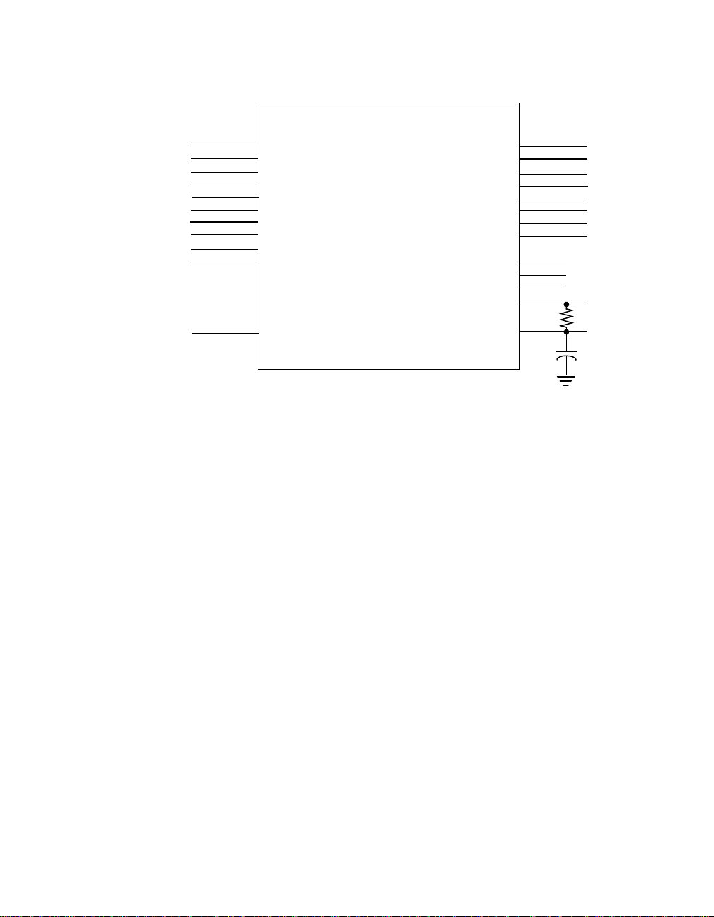
Figure 2.6 Regulated Termination for Ultra2 SC SI
UCC5630
SD0+
SD0
SD1+
SD1
SD2+
SD2
SD3+
SD3
SD4+
SD4
DIFFSENSE connects to the SCSI bus Diffsense line to detect what type of devices (SE,
LVD, or HVD) are connected to the SCSI bus. DISCNCT shuts down the terminator when
it is not at the end of the bus. The disconnect pin low en ables the terminator. Use
additional UCC5630 terminators to terminate the SCSI control signals and wide SCSI
data byte as needed.
4
−
−
−
−
−
LINE1+
5
LINE1
LINE2+
6
LINE2
7
11
LINE3+
12
LINE3
13
LINE4+
14
LINE4
15
LINE5+
16
LINE5
17
DISCNCT
−
−
−
−
−
DIFFSENSE
LINE9
LINE9+
LINE8
LINE8+
LINE7
LINE7+
LINE6
LINE6+
SE
LVD
HVD
DIFF B
−
−
−
−
32
31
30
29
25
24
23
22
33
34
35
20
21
SDP0
SDP0+
−
SD7
SD7+
SD6
−
SD6+
−
SD5
SD5+
−
To LED
Drivers
22 K
0.1
µf
2.2.14 Select/Reselect During Selection/Reselection
In multithreaded SCSI I/O environments, it is not uncommon to be
selected or reselected while trying to perform selection/reselection. This
situation may occur when a SCSI controller (operating in the initiator
mode) tries to select a target and is reselected by another. The Select
SCRIPTS instruction has an alternate address to which the SCRIPTS will
jump when this situation occurs. The analogous situation for target
devices is being selected while trying to perform a reselection.
Once a change in operating mode occurs, the initiator SCRIPTS should
start with a Set Initiator instruction or the target SCRIPTS should start
with a Set Target instruction. The Selection and Reselection Enable bits
(SCSI Chip ID (SCID) bits 5 and 6, respectively) should both be asserted
so that the LSI53C895A may respond as an initiator or as a target. If only
selection is enabled, the LSI53C895A cannot be reselected as an
initiator. There are also status and interrupt bits in the SCSI Interrupt
SCSI Functional Description 2-39
Page 66

Status Zero (SIST0) and SCSI Interrupt Enable Zero (SIEN0) registers,
respectively, indicating that the LSI53C895A has been selected (bit 5)
and reselected (bit 4).
2.2.15 Synchronous Operation
The LSI53C895A can transfer synchronous SCSI data in both the
initiator and target modes. The SCSI Transfer (SXFER) register controls
both the synchronous offset and the transfer period. It may be loaded by
the CPU before SCRIPTS execution begins, from within SCRIPTS using
a Table Indirect I/O instruction, or with a Read-Modify-Write instruction.
The LSI53C895A can receive data from the SCSI bus at a synchronous
transfer period as short as 25 ns, regardless of the transfer period used
to send data. The LSI53C895A can receive data at one-four th of the
divided SCLK frequency. Depending on the SCLK frequency, the
negotiated transfer period, and the synchronous clock divider, the
LSI53C895A can send synchronous data at intervals as short as 25 ns
for Ultra2 SCSI, 50 ns for Ultra SCSI, 100 ns for fast SCSI and 200 ns
for SCSI-1.
2.2.15.1 Determining the Data Transfer Rate
Synchronous data transfer rates are controlled by bits in two different
registers of the LSI53C895A. Following is a brief description of the bits.
Figure 2.7 illustrates the clock division factors used in each register, and
the role of the register bits in determining the transfer rate.
2-40 Functional Description
Page 67
Figure 2.7 Determining the Synchronous Transfer Rate
SCF2 SCF1 SCF0 SCF
0011
0101.5
0112
1003
0003
1014
1106
1118
SCLK
CCF2 CCF1 CCF0 Divisor QCLK (MHz)
0 0 1 1 50.1–66.00
0 1 0 1.5 16.67–25.00
0 1 1 2 25.1–37.50
1 0 0 3 37.51–50.00
0 0 0 3 50.01–66.00
1 0 1 4 75.01–80.00
1 1 0 6 120
1 1 1 8 160
Clock
Quadrupler
QCLK
Divisor
SCF
Divider
CCF
Divider
TP2 TP1 TP0 XFERP
0004
0015
0106
0117
1008
1019
11010
11111
This point
must not
exceed
160 MHz
Example:
QCLK (Quadrupled SCSI Clock) = 160 MHz
SCF = 1 (/1), XFERP = 0 (/4), CCF = 7 (/8)
Synchronous send rate = (QCLK/SCF)/XFERP =
(160/1) /4 = 40 Mbytes/s
Synchronous receive rate = (QCLK /S C F) /4 =
(160/1) /4 = 40 Mbytes/s
Divide by 4
Synchronous
Divider
Asynchronous
SCSI Logic
Divisor
Receive
Clock
Send Clock
(to SCSI Bus)
2.2.15.2 SCSI Control Three (SCNTL3) Register, Bits [6:4] (SCF[2:0])
The SCF[2:0] bits select the factor by which the frequency of SCLK is
divided before being presented to the synchronous SCSI control logic.
The output from this divider controls the rate at which data can be
received; this rate must not exceed 160 MHz. The receive rate of
synchronous SCSI data is one-fourth of the SCF divider output. For
example, if SCLK is 160 MHz and the SCF value is set to divide by one,
then the maximum rate at which data can be received is 40 MHz
(160/(1*4) = 40).
SCSI Functional Description 2-41
Page 68

2.2.15.3 SCSI Control Three (SCNTL3) Register, Bits [2:0] (CCF[2:0])
The CCF[2:0] bits select the factor by which the frequency of SCLK is
divided before being presented to the asynchronous SCSI core logic.
This divider must be set according to the input clock frequency in the
table.
2.2.15.4 SCSI Transfer (SXFER) Register, Bits [7:5] (TP[2:0])
The TP[2:0] divider bits determine the SCSI synchronous transfer period
when sending synchronous SCSI data in either the initiator or target
mode. This value further divides the output from the SCF divider.
2.2.15.5 Ultra2 SCSI Synchronous Data Transfers
Ultra2 SCSI is an extension of the current Ultra SCSI synchronous
transfer specifications. It allows synchronous transfer periods to be
negotiated down as low as 25 ns, which is half the 50 ns period allowed
under Ultra SCSI. This will allow a maximum transfer rate of 80 Mbytes/s
on a 16-bit, LVD SCSI bus. The LSI53C895A has a SCSI clock
quadrupler that must be enabled for the chip to perform Ultra2 SCSI
transfers with a 40 MHz oscillator. In addition, the following bit values
affect the chip’s ability to support Ultra2 SCSI synchronous transfer rates:
• Clock Conversion Factor bits, SCSI Control Three (SCNTL3) register
bits [2:0] and Synchronous Clock Conversion Factor bits, SCNTL3
register bits [6:4]. These fields support a value of 111 (binary),
allowing the 160 MHz SCLK frequency to be divided by 8 for the
asynchronous logic.
• Ultra2 SCSI Enable bit, SCSI Control Three (SCNTL3) register bit 7.
Setting this bit enables Ultra2 SCSI synchronous transfers in
systems that use the internal SCSI clock quadrupler.
• TolerANT Enable bit, SCSI Test Three (STEST3) register bit 7. Active
negation must be enabled for the LSI53C895A to perform Ultra2
SCSI transfers.
Note:
2-42 Functional Description
The clock quadrupler requires a 40 MHz external clock.
LSI Logic software assumes that the LSI53C895A is
connected to a 40 MHz external clock, which is quadrupled
to achieve Ultra2 SCSI transfer rates.
Page 69

2.2.16 Interrupt Handling
The SCRIPTS processors in the LSI53C895A perform most functions
independently of the host microprocessor. However, certain interrupt
situations must be handled by the external microprocessor. This section
explains all aspects of interrupts as they apply to the LSI53C895A.
2.2.16.1 Polling and Hardware Interrupts
The external microprocessor is informed of an interrupt condition by
polling or hardware interrupts. Polling means that the microprocessor
must continually loop and read a register until it detects a bit that is set
indicating an interrupt. This method is the fastest, but it wastes CPU time
that could be used for other system tasks. The preferred method of
detecting interrupts in most systems is hardware interrupts. In this case,
the LSI53C895A asserts the Interrupt Request (IRQ/) line that interrupts
the microprocessor, causing the microprocessor to execute an interrupt
service routine. A hybrid approach would use hardware interrupts for
long waits, and use polling for short waits.
2.2.16.2 Registers
The registers in the LSI53C895A that are used for detecting or defining
interrupts are Interrupt Status Zero (ISTAT0), Interrupt Status One
(ISTAT1), Mailbox Zero (MBOX0), Mailbox One (MBOX1), SCSI Interrupt
Status Zero (SIST0), SCSI Interrupt Status One (SIST1), DMA Status
(DSTAT), SCSI Interrupt Enable Zero (SIEN0), SCSI Interrupt Enable
One (SIEN1), DMA Control (DCNTL),andDMA Interrupt Enable (DIEN).
ISTAT – The ISTAT register includes the Interrupt Status Zero (ISTAT0),
Interrupt Status One (ISTAT1), Chip Test Zero (CTEST0),andMailbox
One (MBOX1) registers. It is the only register that can be accessed as a
slave during the SCRIPTS operation. Therefore, it is the register that is
polled when polled interrupts are used. It is also the first register that
should be read after the IRQ/ pin is asserted in association with a
hardware interrupt. The INTF (Interrupt-on-the-Fly) bit should be the first
interrupt serviced. It must be written to one to be cleared. This interrupt
must be cleared before servicing any other interrupts.
See Register 0x14, Interrupt Status Zero (ISTAT0) register, Bit 5 Signal
process in Chapter 4, “Registers,” for additional information.
SCSI Functional Description 2-43
Page 70

The host (C Code) or the SCRIPTS code could potentially try to access
the mailbox bits at the same time.
If the SIP bit in the Interrupt Status Zero (ISTAT0) register is set, then a
SCSI-type interrupt has occurred and the SCSI Interrupt Status Zero
(SIST0) and SCSI Interrupt Status One (SIST1) registers should be read.
If the DIP bit in the Interrupt Status Zero (ISTAT0) register is set, then a
DMA-type interrupt has occurred and the DMA Status (DSTAT) register
should be read.
SCSI-type and DMA-type interrupts may occur simultaneously, so in
some cases both SIP and DIP may be set.
SIST0 and SIST1 – The SCSI Interrupt Status Zero (SIST0) and SCSI
Interrupt Status One (SIST1) registers contain SCSI-type interrupt bits.
Reading these registers determines which condition orconditions caused
the SCSI-type interrupt, and clears that SCSI interrupt condition.
If the LSI53C895A is receiving data from the SCSI bus and a fatal
interrupt condition occurs, the chip attempts to send the contents of the
DMA FIFO to memory before generating the interrupt.
If the LSI53C895A is sending data to the SCSI bus and a fatal SCSI
interrupt condition occurs, data could be left in the DMA FIFO. Because
of this the DMA FIFO Empty (DFE) bit in DMA Status (DSTAT) should be
checked.
If this bit is cleared, set the CLF (Clear DMA FIFO) and CSF (Clear SCSI
FIFO) bits before continuing. The CLF bit is bit 2 in Chip Test Three
(CTEST3). The CSF bit is bit 1 in SCSI Test Three (STEST3).
DSTAT – The DMA Status (DSTAT) register contains the DMA-type
interrupt bits. Reading this register determines which condition or
conditions caused the DMA-type interrupt, and clears that DMA interrupt
condition. Bit 7 in DSTAT, DFE, is purely a status bit; it will not generate
an interrupt under any circumstances and will not be cleared when read.
DMA interrupts flush neither the DMA nor SCSI FIFOs before generating
the interrupt, so the DFE bit in the DMA Status (DSTAT) register should
be checked after any DMA interrupt.
2-44 Functional Description
Page 71

If the DFE bit is cleared, then the FIFOs must be cleared by setting the
CLF (Clear DMA FIFO) and CSF (Clear SCSI FIFO) bits, or flushed by
setting the FLF (Flush DMA FIFO) bit.
SIEN0 and SIEN1 – The SCSI Interrupt Enable Zero (SIEN0) and SCSI
Interrupt Enable One (SIEN1) registers are the interrupt enable registers
for the SCSI interrupts in SCSI Interrupt Status Zero (SIST0) and SCSI
Interrupt Status One (SIST1).
DIEN – The DMA Interrupt Enable (DIEN) register is the interrupt enable
register for DMA interrupts in DMA Status (DSTAT).
DCNTL – When bit 1 in the DMA Control (DCNTL) register is set, the
IRQ/ pin is not asserted when an interrupt condition occurs. The interrupt
is not lost or ignored, but is merely masked at the pin. Clearing this bit
when an interrupt is pending immediately causes the IRQ/ pin to assert.
As with any register other than ISTAT , this register cannot be accessed
except by a SCRIPTS instruction during SCRIPTS execution.
2.2.16.3 Fatal vs. Nonfatal Interrupts
A fatal interrupt, as the name implies, always causes the SCRIPTS to
stop running. All nonfatal interrupts become fatal when they are enabled
by setting the appropriate interrupt enable bit. Interrupt masking is
discussed in Section 2.2.16.4, “Masking.” All DMA interrupts (indicated
by the DIP bit in ISTAT and one or more bits in DMA Status (DSTAT)
being set) are fatal.
Some SCSI interrupts (indicated by the SIP bit in the Interrupt Status
Zero (ISTAT0) and one or more bits in SCSI Interrupt Status Zero
(SIST0) or SCSI Interrupt Status One (SIST1) being set) are nonfatal.
When the LSI53C895A is operating in the Initiator mode, only the
Function Complete (CMP), Selected (SEL), Reselected (RSL), General
Purpose Timer Expired (GEN), and Handshake-to-Handshake Timer
Expired (HTH) interrupts are nonfatal.
When operating in the Target mode, CMP, SEL, RSL, Target mode:
SATN/ active (M/A), GEN, and HTH are nonfatal. Refer to the description
for the Disable Halt on a Parity Error or SATN/ active (Target Mode Only)
(DHP) bit in the SCSI Control One (SCNTL1) register to configure the
SCSI Functional Description 2-45
Page 72

2.2.16.4 Masking
chip’s behavior when the SATN/ interrupt is enabled during Target mode
operation. The Interrupt-on-the-Fly interrupt is also nonfatal, since
SCRIPTS can continue when it occurs.
The reason for nonfatal interrupts is to prevent the SCRIPTS from
stopping when an interrupt occurs that does not require service from the
CPU. This prevents an interrupt when arbitration is complete (CMP set),
when the LSI53C895A is selected or reselected (SEL or RSL set), when
the initiator asserts A TN (target mode: SATN/ active), or when the
General Purpose or Handshake-to-Handshake timers expire. These
interrupts are not needed for events that occur during high-level
SCRIPTS operation.
Masking an interrupt means disabling or ignoring that interrupt. Interrupts
canbemaskedbyclearingbitsintheSCSI Interrupt Enable Zero
(SIEN0) and SCSI Interrupt Enable One (SIEN1) (for SCSI interrupts)
registers or DMA Interrupt Enable (DIEN) (for DMA interrupts) register.
How the chip responds to masked interrupts depends on: whether polling
or hardware interrupts are being used; whether the interrupt is fatal or
nonfatal; and whether the chip is operating in the Initiator or Target mode.
If a nonfatal interrupt is masked and that condition occurs, the SCRIPTS
do not stop, the appropriate bit in the SCSI Interrupt Status Zero (SIST0)
or SCSI Interrupt Status One (SIST1) is still set, the SIP bit in the
Interrupt Status Zero (ISTAT0) is not set, and the IRQ/ pin is not
asserted.
If a fatal interrupt is masked and that condition occurs, then the SCRIPTS
still stop, the appropriate bit in the DMA Status (DSTAT), SCSI Interrupt
Status Zero (SIST0),orSCSI Interrupt Status One (SIST1) register is
set, and the SIP or DIP bit in the Interrupt Status Zero (ISTAT0) register
is set, but the IRQ/ pin is not asserted.
Interrupts can be disabled by setting SYNC_IRQD bit 0 in the Interrupt
Status One (ISTAT1) register. If an interrupt is already asserted and
SYNC_IRQD is then set, the interrupt will remain asserted until serviced.
At this point, the IRQ/ pin is blocked for future interrupts until this bit is
cleared. When the LSI53C895A is initialized, enable all fatal interrupts if
you are using hardware interrupts. If a fatal interrupt is disabled and that
2-46 Functional Description
Page 73

interrupt condition occurs, the SCRIPTS halt and the system never
knows it unless it times out and checks the ISTAT register after a certain
period of inactivity.
If you are polling the ISTAT instead of using hardware interrupts, then
masking a fatal interrupt makes no difference since the SIP and DIP bits
in the Interrupt Status Zero (ISTAT0) inform the system of interrupts, not
the IRQ/ pin.
Masking an interrupt after IRQ/ is asserted does not cause deassertion
of IRQ/.
2.2.16.5 Stacked Interrupts
The LSI53C895A will stack interrupts if they occur one after the other. If
the SIP or DIP bits in the ISTAT register are set (first level), then there is
already at least one pending interrupt, and any future interrupts are
stacked in extra registers behind the SCSI Interrupt Status Zero (SIST0),
SCSI Interrupt Status One (SIST1), and DMA Status (DSTAT) registers
(second level). When two interrupts have occurred and the two levels of
the stack are full, any further interrupts set additional bits in the extra
registers behind SCSI Interrupt Status Zero (SIST0), SCSI Interrupt
Status One (SIST1), and DMA Status (DSTAT). When the first level of
interrupts are cleared, all the interrupts that came in afterward move into
SIST0, SIST1, and DSTAT. After the first interrupt is cleared by reading
the appropriate register, the IRQ/ pin is deasserted for a minimum of
three CLKs; the stacked interrupts move into SIST0, SIST1, or DSTAT;
and the IRQ/ pin is asserted once again.
Since a masked nonfatal interrupt does not set the SIP or DIP bits,
interrupt stacking does not occur. A masked, nonfatal interrupt still posts
the interrupt in SIST0, but does not assert the IRQ/ pin. Since no
interrupt is generated, future interrupts move into SCSI Interrupt Status
Zero (SIST0) or SCSI Interrupt Status One (SIST1) instead of being
stacked behind another interrupt. When another condition occurs that
generates an interrupt, the bit corresponding to the earlier masked
nonfatal interrupt is still set.
A related situation to interrupt stacking is when two interrupts occur
simultaneously. Since stacking does not occur until the SIP or DIP bits
are set, there is a small timing window in which multiple interrupts can
SCSI Functional Description 2-47
Page 74

occur but are not stacked. These could be multiple SCSI interrupts (SIP
set), multiple DMA interrupts (DIP set), or multiple SCSI and multiple
DMA interrupts (both SIP and DIP set).
As previously mentioned, DMA interrupts do not attempt to flush the
FIFOs before generating the interrupt. It is important to set either the
Clear DMA FIFO (CLF) and Clear SCSI FIFO (CSF) bits if a DMA
interrupt occurs and the DMA FIFO Empty (DFE) bit is not set. This is
because any future SCSI interrupts are not posted until the DMA FIFO
is cleared of data. These ‘locked out’ SCSI interrupts are posted as soon
as the DMA FIFO is empty.
2.2.16.6 Halting in an Orderly Fashion
When an interrupt occurs, the LSI53C895A attempts to halt in an orderly
fashion.
• If the interrupt occurs in the middle of an instruction fetch, the fetch
is completed, except in the case of a Bus Fault. Execution does not
begin, but the DMA SCRIPTS Pointer (DSP) points to the next
instruction since it is updated when the current instruction is fetched.
• If the DMA direction is a write to memory and a SCSI interrupt
occurs, the LSI53C895A attempts to flush the DMA FIFO to memory
before halting. Under any other circumstances only the current cycle
is completed before halting, so the DFE bit in DMA Status (DSTAT)
register should be checked to see if any data remains in the DMA
FIFO.
• SCSI SREQ/SACK handshakes that have begun are completed
before halting.
• The LSI53C895A attempts to clean up any outstanding synchronous
offset before halting.
• In the case of Transfer Control Instructions, once instruction
execution begins it continues to completion before halting.
• If the instruction is a JUMP/CALL WHEN/IF <phase>, the DMA
SCRIPTS Pointer (DSP) is updated to the transfer address before
halting.
• All other instructions may halt before completion.
2-48 Functional Description
Page 75

2.2.16.7 Sample Interrupt Service Routine
The following is a sample of an interrupt service routine for the
LSI53C895A. It can be repeated during polling or should be called when
the IRQ/ pin is asserted during hardware interrupts.
1. Read Interrupt Status Zero (ISTAT0).
2. If the INTF bit is set, it must be written to a one to clear this status.
3. If only the SIP bit is set, read SCSI Interrupt Status Zero (SIST0) and
SCSI Interrupt Status One (SIST1) to clear the SCSI interrupt
condition and get the SCSI interrupt status. The bits in the SIST0
and SIST1 tell which SCSI interrupts occurred and determine what
action is required to service the interrupts.
4. If only the DIP bit is set, read DMA Status (DSTAT) to clear the
interrupt condition and get the DMA interrupt status. The bits in
DSTAT tells which DMA interrupts occurred and determine what
action is required to service the interrupts.
5. If both the SIP and DIP bits are set, read SCSI Interrupt Status Zero
(SIST0), SCSI Interrupt Status One (SIST1),andDMA Status
(DSTAT) to clear the SCSI and DMA interrupt condition and get the
interrupt status. If using 8-bit reads of the SIST0, SIST1, and DSTAT
registers to clear interrupts, insert a 12 CLK delay between the
consecutive reads to ensure that the interrupts clear properly. Both
the SCSI and DMA interrupt conditions should be handled before
leaving the interrupt service routine. It is recommended that the DMA
interrupt is serviced before the SCSI interrupt, because a serious
DMA interrupt condition could influence how the SCSI interrupt is
acted upon.
6. When using polled interrupts, go back to Step 1 before leaving the
interrupt service routine, in case any stacked interrupts moved in
when the first interrupt was cleared. When using hardware interrupts,
the IRQ/ pin is asserted again if there are any stacked interrupts.
This should cause the system to re-enter the interrupt service
routine.
SCSI Functional Description 2-49
Page 76

2.2.17 Interrupt Routing
This section documents the recommended approach to RAID ready
interrupt routing for the LSI53C895A. In order to be compatible with AMI
RAID upgrade products and the LSI53C895A, the following requirements
must be met:
• When a RAID upgrade card is installedin the upgrade slot, interrupts
from the mainboard SCSI controller(s) assigned to the RAID upgrade
card must be routed to INTB/, INTC/ and INTD/ of the upgrade slot
and isolated from the mainboard interrupt controller. The system
processor must not see interrupts from the SCSI controllers that are
to be serviced by the RAID upgrade card. An upgradeslot is one that
is connected to the interrupt routing logic for mainboard SCSI
device(s). When a PCI RAID upgrade board is installed into the
system, it would be plugged into this slot if it is to control mainboard
SCSI device(s).
• When a RAID upgrade card is not installed, interrupts from a SCSI
core must not be presented to the system’s interrupt controller using
multiple interrupt inputs.
The LSI53C895A supports four different interrupt routing modes.
Additional information for these modes may be found in the
Register 0x4D SCSI Test One (STEST1) description in Chapter 4,
“Registers.” The interrupt routing mode is selected using bits [1:0] in the
STEST1 register. Mode 0 is the default mode and is compatible with AMI
RAID upgrade products. In this mode, interrupts are presented on IRQ/
and ALR_IRQ/.
If INTB/, INTC/ or INTD/ of the PCI RAID upgrade slot is used in the
interrupt routing scheme, it cannot be used when a non-RAID upgrade
card is installed in the slot. If this restriction is not acceptable, additional
buffer logic must be implemented on the mainboard. As long as the
interrupt routing requirements stated above are satisfied, a mainboard
designer could implement this design with external logic.
There can only be one entity controlling a mainboard LSI53C895A or
conflicts will occur. Typically, SCSI BIOS and an operating system driver
control the LSI53C895A. When allocated to a RAID adapter, however, a
mechanism is implemented to prevent the SCSI BIOS and operating
system driver from trying to access the chip. The mainboard designer
has several options, listed below.
2-50 Functional Description
Page 77

The first option is to have the LSI53C895A load its PCI Subsystem ID
using a serial EPROM on power-up. If bit 15 in this ID is set, the
LSI Logic BIOS and operating system drivers (not all versions support
this capability) will ignore the chip. This makes it possible to control the
assignment of the mainboard SCSI controller using a configuration utility.
The second option is to provide mainboard and system BIOS support for
NVS. You can then enable or disable the LSI53C895A using the SCSI
BIOS configuration utility. Not all versions of the LSI Logic drivers support
this capability.
The third option is to have the system BIOS not report the existence of
the SCSI controller when the SCSI BIOS and operating systems make
PCI BIOS calls. This approach requires modifications to the system BIOS
and assumes the operating system uses PCI BIOS calls when searching
for PCI devices.
2.2.18 Chained Block Moves
Since the LSI53C895A has the capability to transfer 16-bit wide SCSI
data, a unique situation occurs when dealing with odd bytes. The
Chained Move (CHMOV) SCRIPTS instruction along with the Wide SCSI
Send (WSS) and Wide SCSI Receive (WSR) bits in the SCSI Control
Two (SCNTL2) register are used to facilitate these situations. The
Chained Block Move instruction is illustrated in Figure 2.8.
SCSI Functional Description 2-51
Page 78

Figure 2.8 Block Move and Chained Block Move Instructions
Host Memory
0x03
0x07 0x06 0x05 0x04
0x0B 0x0A 0x09 0x08
0x0F 0x0E 0x0D 0x0C
0x13 0x12 0x11 0x10
0x02 0x01 0x00
SCSI Bus
0x04 0x03
0x06 0x05
0x09
0x0B 0x0A
0x0D 0x0C
0x07
32 Bits 16 Bits
CHMOV 5, 3 when Data_Out
Moves five bytes from address 0x03 in the host memory to the SCSI bus.
Bytes 0x03, 0x04, 0x05, and 0x06 are moved and byte 0x07 remains in
the low-order byte of the SCSI Output Data Latch (SODL) register and
ismarriedwiththefirstbyteofthefollowingMOVEinstruction.
MOVE 5, 9 when Data_Out
Moves five bytes from address 0x09 in the host memory to the SCSI bus.
2.2.18.1 Wide SCSI Send Bit
The WSS bit is set whenever the SCSI controller is sending data
(Data-Out for initiator or Data-In for target) and the controller detects a
partial transfer at the end of a chained Block Move SCRIPTS instruction
2-52 Functional Description
Page 79

(this flag is not set if a normal Block Move instruction is used). Under this
condition, the SCSI controller does not send the low-order byte of the last
partial memory transfer across the SCSI bus. Instead, the low-order byte
is temporarily stored in the lower byte of the SCSI Output Data Latch
(SODL) register and the WSS flag is set. The hardware uses the WSS
flag to determine what behavior must occur at the start of the next data
send transfer. When the WSS flag is set at the start of the next transfer,
the first byte (the high-order byte) of the next data send transfer is
“married” with the stored low-order byte in the SODL register; and the
two bytes are sent out across the bus, regardless of the type of Block
Move instruction (normal or chained). The flag is automatically cleared
when the “married” word is sent. The flag is alternately cleared through
SCRIPTS or by the microprocessor. Also, the microprocessor or
SCRIPTS can use this bit for error detection and recovery purposes.
2.2.18.2 Wide SCSI Receive Bit
The WSR bit is set whenever the SCSI controller is receiving data
(Data-In for initiator or Data-Out for target) and the controller detects a
partial transfer at the end of a block move or chained block move
SCRIPTS instruction. When WSR is set, the high-order byte of the last
SCSI bus transfer is not transferred to memory . Instead, the byte is
temporarily stored in the SCSI Wide Residue (SWIDE) register. The
hardware uses the WSR bit to determine what behavior must occur at
the start of the next data receive transfer. The bit is automatically cleared
at the start of the next data receive transfer. The bit can alternatively be
cleared by the microprocessor or through SCRIPTS. Also, the
microprocessor or SCRIPTS can use this bit for error detection and
recovery purposes.
2.2.18.3 SWIDE Register
This register stores data for partial byte data transfers. For receive data,
the SCSI Wide Residue (SWIDE) register holds the high-order byte of a
partial SCSI transfer which has not yet been transferred to memory. This
stored data may be a residue byte (and therefore ignored) or it may be
valid data that is transferred to memory at the beginning of the next Block
Move instruction.
SCSI Functional Description 2-53
Page 80

2.2.18.4 SODL Register
For send data, the low-order byte of the SCSI Output Data Latch (SODL)
register holds the low-order byte of a partial memory transfer which has
not yet been transferred across the SCSI bus. This stored data is usually
“married” with the first byte of the next data send transfer , and both bytes
are sent across the SCSI bus at the start of the next data send block
move command.
2.2.18.5 Chained Block Move SCRIPTS Instruction
A chained Block Move SCRIPTS instruction is primarily used to transfer
consecutive data send or data receive blocks. Using the chained Block
Move instruction facilitates partial receive transfers and allows correct
partial send behavior without additional opcode overhead. Behavior of
the chained Block Move instruction varies slightly for sending and
receiving data.
For receive data (Data-In for initiator or Data-Out for target), a chained
Block Move instruction indicates that if a partial transfer occurred at the
end of the instruction, the WSR flag is set. The high-order byte of the
last SCSI transfer is stored in the SCSI Wide Residue (SWIDE) register
rather than transferred to memory. The contents of the SWIDE register
should be the first byte transferred to memory at the start of the chained
Block Move data stream. Since the byte count always represents data
transfers to/from memory (as opposed to the SCSI bus), the byte
transferred out of the SCSI Wide Residue (SWIDE) register is one of the
bytes in the byte count. If the WSR bit is cleared when a receive data
chained Block Move instruction is executed, the data transfer occurs
similar to that of the regular Block Mov e instruction. Whether the WSR
bit is set or cleared, when a normal block move instruction is e xecuted,
the contents of the SCSI Wide Residue (SWIDE) register are ignored
and the transfer takes place normally. For “N” consecutive wide data
receive Block Move instructions, the 2nd through the Nth Block Move
instructions should be chained block moves.
For send data (Data-Out for initiator or Data-In for target), a chained
Block Move instruction indicates that if a partial transfer terminates the
chained block move instruction, the last low-order byte (the partial
memorytransfer)shouldbestoredinthelowerbyteoftheSCSI Output
Data Latch (SODL) register and not sent across the SCSI bus. Without
the chained Block Move instruction, the last low-order byte would be sent
across the SCSI bus. The starting byte count represents data bytes
2-54 Functional Description
Page 81

transferred from memory but not to the SCSI bus when a partial transfer
exists. For example, if the instruction is an Initiator chained Block Move
Data Out of five bytes (and WSS is not previously set), five bytes are
transferred out of memory to the SCSI controller, four bytes are
transferred from the SCSI controller across the SCSI bus, and one byte
is temporarily stored in the lower byte of the SCSI Output Data Latch
(SODL) register waiting to be married with the first byte of the next Block
Move instruction. Regardless of whether a chained Block Move or normal
Block Move instruction is used, if the WSS bit is set at the start of a data
send command, the first byte of the data send command is assumed to
be the high-order byte and is “married” with the low-order byte stored in
the lower byte of the SCSI Output Data Latch (SODL) register before the
two bytes are sent across the SCSI bus. For “N” consecutive wide data
send Block Move commands, the first through the (N
instructions should be Chained Block Moves.
2.3 Parallel ROM Interface
The LSI53C895A supports up to one megabyte of external memory in
binary increments from 16 Kbytes, to allow the use of expansion ROM
for add-in PCI cards. This interface is designed for low speed operations
such as downloading instruction code from ROM; it is not intended for
dynamic activities such as executing instructions.
th
– 1) Block Move
System requirements include the LSI53C895A, two or three external
8-bit address holding registers (HCT273 or HCT374), and the
appropriate memory device. The 4.7 k
require HC or HCT external components to be used. If in-system Flash
ROM updates are required, a 7406 (high voltage open collector inverter),
a MTD4P05, and several passive components are also needed. The
memory size and speed is determined by pull-up resistors on the
8-bit bidirectional memory bus at power-up. The LSI53C895A senses this
bus shortly after the release of the Reset signal and configures the
Expansion ROM Base Address register and the memory cycle state
machines for the appropriate conditions.
The external memory interface works with a variety of ROM sizes and
speeds. An example set of interface drawings is in Appendix B, “External
Memory Interface Diagram Examples.”
Parallel ROM Interface 2-55
Ω pull-up resistors on the MAD bus
Page 82

The LSI53C895A supports a variety of sizes and speeds of expansion
ROM, using pull-down resistors on the MAD[3:0] pins. The encoding of
pins MAD[3:1] allows the user to define how much external memory is
available to the LSI53C895A. Table 2.7 shows the memory space
associated with the possible values of MAD[3:1]. The MAD[3:1] pins are
fully described in Chapter 3, “Signal Descriptions.”
Table 2.7 Parallel ROM Support
MAD[3:1] Av ailable Memory Space
000 16 Kbytes
001 32 Kbytes
010 64 Kbytes
011 128 Kbytes
100 256 Kbytes
101 512 Kbytes
110 1024 Kbytes
111 no external memory present
To use one of the configurations mentioned above in a host adapter
board design, put 4.7 k
corresponding to the available memory space. For example, to connect
to a 64 Kbyte external ROM, use a pull-up on MAD2. If the external
memory interface is not used, MAD[3:1] should be pulled HIGH.
Note:
There are internal pull-downs on all of the MAD bus
signals.
The LSI53C895A allows the system to determine the size of the available
external memory using the Expansion ROM Base Address register in the
PCI configuration space. For more information on how this works, refer
to the PCI specification or the Expansion ROM Base Address register
description in Chapter 4, “Registers.”
MAD0 is the slow ROM pin. When pulled up, it enables two extra clock
cycles of data access time to allow use of slower memory devices. The
external memory interface also supports updates to flash memory.
2-56 Functional Description
Ω pull-up resistors on the MAD pins
Page 83

2.4 Serial EEPROM Interface
The LSI53C895A implements an interface that allows attachment of a
serial EEPROM device to the GPIO0 and GPIO1 pins. There are two
modes of operation relating to the serial EEPROM and the Subsystem
ID and Subsystem Vendor ID registers. These modes are programmable
through the MAD7 pin which is sampled at power-up.
Also, the LSI53C895A implements a method for programming the
Subsystem ID and Subsystem Vendor ID registers without a serial
EEPROM download. Please see Section 2.5, “Alternative SSVID/SSID
Loading Mechanism,” for additional information.
2.4.1 Default Download Mode
In this mode, MAD7 is pulled down internally, GPIO0 is the serial data
signal (SDA) and GPIO1 is the serial clock signal (SCL). Certain data in
the serial EEPROM is automatically loaded into chip registers at
power-up.
The format of the serial EEPROM data is defined in Table 2.8.Ifthe
download is enabled and an EEPROM is not present, or the checksum
fails, the Subsystem ID and Subsystem Vendor ID registers read back all
zeros. At power-up, only five bytes are loaded into the chip from locations
0xFB through 0xFF.
The Subsystem ID and Subsystem Vendor ID registers are read only, in
accordance with the PCI specification, with a default value of all zeros if
the download fails.
Serial EEPROM Interface 2-57
Page 84

Table 2.8 Mode A Serial EEPROM Data Format
Byte Name Description
0xFB SVID(0) Subsystem Vendor ID, LSB. This byte is loaded into the least significant
0xFC SVID(1) Subsystem Vendor ID, MSB. This byte is loaded into the most significant
0xFD SID(0) Subsystem ID, LSB. This byte is loaded into the least significant byte of
0xFE SID(1) Subsystem ID, MSB. This byte is loaded into the most significant byte of
0xFF CKSUM Checksum. This 8 bit checksum is formed by adding, bytewise, each byte
0x100–0xEOM UD User Data.
byte of the Subsystem Vendor ID register in the appropriate PCI
configuration space at chip power-up.
byte of the Subsystem Vendor ID register in the appropriate PCI
configuration space at chip power-up.
the Subsystem ID register in the appropriate PCI configuration space at
chip power-up.
the Subsystem ID register in the appropriate PCI configuration space at
chip power-up.
contained in locations 0x00–0x03 to the seed value 0x55, and then taking
the 2’s complement of the result.
2.4.2 No Download Mode
When MAD7 is pulled up through an external resistor, the automatic
download is disabled and no data is automatically loaded into chip
registers at power-up. The Subsystem ID and Subsystem Vendor ID
registers are read only, per the PCI specification, with a default value of
0x1000 and 0x1000 respectively.
2.5 Alternative SSVID/SSID Loading Mechanism
Programming the PCI Subsystem ID and Subsystem Vendor ID registers
can be accomplished in the LSI53C895A without the use of a serial
EEPROM. This alternative loading mechanism is the only way to set the
SSVID/SSID registers to something other than the default value, except
through Serial EEPROM download.
Please see Section 2.4, “Serial EEPROM Interface,” for additional
information.
2-58 Functional Description
Page 85

An additional register, the Subsystem ID Access, is located in the PCI
configuration space at offset 0x48–0x4B. This is a 32-bit write only
register that always reads back a value of 0x00000000. Once enabled
and unlocked using a write of three specific byte values to offset 0x48, a
write to this register is shadowed into the PCI Subsystem register at
offset 0x2C. Any data written to the register cannot be read back through
the register, it always reads back 0x00000000.
To disable the Subsystem ID Access, the MAD4 pin must be pulled
HIGH. (Note: There is an internal pull-down on the MAD4 pin.) A logical
zero (0) on this pin will enable the Subsystem ID Access register,
allowing it to be unlocked by writing the proper three byte sequence to
offset 0x48. A logical one (1) on this pin will disable the Subsystem ID
Access register.
Once the Subsystem ID Access register is enabled, a sequence of three
byte writes to offset 0x48 will allow a 32-bitsubsystem value to be written
to offset 0x48–0x4B which will then be shadowed into the PCI
Subsystem register at offset 0x2C–0x2F. The three byte values that must
be written are 0x53, 0x59, 0x4D (ASCII) in this order. Once this
sequence is written, the next write to offset 0x48–0x4B is shadowed into
the Subsystem register. At no time can any of the data written to the
Subsystem ID register be read back. The register alwa ys reads back
zeros. In addition, any reads to offset 0x48 between writes of the unlock
code or the actual subsystem value will reset the internal state machine
requiring the sequence be restarted from the beginning. Byte, word, or
Dword writes are allowed during the unlock sequence with the other byte
lanes (0x49, 0x4A, and 0x4B) being don’t cares. Once the subsystem
valueiswrittenintotheSubsystem ID Access register, the register will
again lock itself and the three byte sequence must be repeated to allow
further writes to this register to be shadowed into the Subsystem register
at offset 0x2C–0x2F.
If the Subsystem ID Access register writes a new value to the Subsystem
register (0x2C), the Subsystem register retains that value until the
Alternative SSVID/SSID Loading Mechanism is used again to change the
value. Prior to the first unlock of the Subsystem ID Access register after
a power-on, the Subsystem register presents the value determined by
the Subsystem ID and Subsystem Vendor ID described in the section
above. This allows an autodownload from a serial EEPROM to change
the v alue of the Subsystem register. Additionally, that value may be
overridden by writing to the Subsystem ID Access register. The serial
Alternative SSVID/SSID Loading Mechanism 2-59
Page 86

EEPROM value is always the first value loaded (if that mechanism is
enabled). The system would then have the opportunity to override the
value loaded from the serial EEPROM.
Below is an example of how the enabling sequence occurs:
1. Ensure that the MAD4 pin is at a logical zero during power-up of the
LSI53C895A. This enables the Subsystem ID Access register.
2. Write value 0x53 to PCI offset 0x48 using a PCI Configuration Write.
3. Write value 0x59 to PCI offset 0x48 using a PCI Configuration Write.
4. Write value 0x4D to PCI offset 0x48 using a PCI Configuration Write.
The Subsystem ID Access register is now unlocked for a single write.
5. Write the desired subsystem value to offset 0x48–0x4B using a PCI
Configuration Write.
6. Read back the Subsystem register at PCI offset 0x2C–0x2F to verify
the new value written in Step 5.
7. Return to Step 2 to change the subsystem value at offset 0x2C.
Note:
The following events will reset the lock mechanism:
During the unlock sequence byte, word, or Dword writes
are allowed, but with the other byte lanes being don’t cares.
• APCIReset.
• Any reads to offset 0x48–0x4B between Steps 2 through 5.
• Any writes other than the specified data values between Steps 2
through 4.
• The write of the subsystem value in Step 5.
2.6 Power Management
The LSI53C895A complies with the PCI Bus Pow er Management
Interface Specification, Revision 1.1. The PCI Function Power States D0,
D1, D2, and D3 are defined in that specification.
D0 is the maximum powered state, and D3 is the minimum powered
state. Power state D3 is further categorized as D3hot or D3cold. A
function that is powered off is said to be in the D3cold power state.
2-60 Functional Description
Page 87

The LSI53C895A power states shown in Table 2.9 are independently
controlled through two power state bits that are located in the PCI Power
Management Control/Status (PMCSR) register 0x44.
Table 2.9 Power S tates
Configuration Register 0x44
Although the PCI Bus Power Management Interface Specification does
not allow power state transitions D2 to D1, D3 to D2, or D3 to D1, the
LSI53C895A hardware places no restriction on transitions between
power states.
As the device transitions from one power level to a lower one, the
attributes that occur from the higher power state level are carried over
into the lower power state level. For example, D1 disables the SCSI CLK.
Therefore, D2 will include this attribute as well as the attributes defined
in the Power State D2 section. The PCI Function Power States D0, D1,
D2, and D3 are described below. Power state actions are separate for
each function.
2.6.1 Power State D0
Bits [1:0] Power State Function
00 D0 Maximum Power
01 D1 Disables SCSI Clock
10 D2 Coma Mode
11 D3 Minimum Power
Power state D0 is the maximum power state and is the power-up default
state. The LSI53C895A is fully functional in this state.
2.6.2 Power State D1
Power state D1 is a lower power state than D0. In this state, the
LSI53C895A core is placed in the snooze mode and the SCSI CLK is
disabled. In the snooze mode, a SCSI reset does not generate an IRQ/
signal. However, the SCSI CLK is still disabled.
Power Management 2-61
Page 88

2.6.3 Power State D2
Power state D2 is a lower power state than D1. In this state the
LSI53C895A core is placed in the coma mode. The following PCI
Configuration Space command register enable bits are suppressed:
• I/O Space Enable
• Memory Space Enable
• Bus Mastering Enable
• SERR/Enable
• Enable Parity Error Response
Thus, the memory and I/O spaces cannot be accessed, and the
LSI53C895A cannot be a PCI bus master. Furthermore, all interrupts are
disabled when in power state D2. If changed from power state D2 to
power state D0, the previous values of the PCI command register are
restored. Also, any pending interrupts before the function entered power
state D2 are asserted.
2.6.4 Power State D3
Power state D3 is the minimum power state, which includes settings
called D3hot and D3cold. D3hot allows the device to transition to D0
using software. The LSI53C895A is considered to be in power state
D3cold when power is removed from the device. D3cold can transition to
D0 by applying V
soft reset is continually asserted while in power state D3, which clears
all pending interrupts and 3-states the SCSI bus. In addition, the device's
PCI command register is cleared and the Clock Quadrupler is disabled,
which results in additional power savings.
and resetting the device. Furthermore, the device's
CC
2-62 Functional Description
Page 89

Chapter 3
Signal Descriptions
This chapter presents the LSI53C895A pin configuration and signal
definitions using tables and illustrations. The LSI53C895A comes in a
208 PQFP and a 272 BGA package. Definitions in the signal description
tables are for both the 208 PQFP and the 272 BGA. This chapter
contains the following sections:
• Section 3.1, “LSI53C895A Functional Signal Grouping”
• Section 3.2, “Signal Descriptions”
• Section 3.3, “PCI Bus Interface Signals”
• Section 3.4, “SCSI Bus Interface Signals”
• Section 3.5, “Flash ROM and Memory Interface Signals”
• Section 3.6, “T est Interface Signals”
• Section 3.7, “Power and Ground Signals”
• Section 3.8, “MAD Bus Programming”
A slash (/) at the end of a signal name indicates that the active state
occurs when the signal is at a LOW voltage. When the slash is absent,
the signal is active at a HIGH voltage.
LSI53C895A PCI to Ultra2 SCSI Controller 3-1
Page 90

3.1 LSI53C895A Functional Signal Grouping
Figure 3.1 presents the LSI53C895A signals by functional group.
Figure 3.1 LSI53C895A Functional Signal Grouping
LSI53C895A
System
CLK
RST/
SCLK
PCI
Bus
Interface
Address
and
Data
Interface
Control
Arbitration
Error
Reporting
Interrupt
SCSI
Function
GPIO
Flash ROM
and Memory
Interface
AD[31:0]
C_BE[3:0]
PAR
FRAME/
TRDY/
IRDY/
STOP/
DEVSEL/
IDSEL
REQ/
GNT/
PERR/
SERR/
IRQ/
ALT_IRQ/
GPIO0_FETCH/
GPIO1_MASTER
GPIO2
GPIO3
GPIO4
GPIO5
GPIO6
GPIO7
GPIO8
MWE/
MCE/
MOE/
MAC/_TESTOUT
MAS0/
MAS1/
MAD[7:0]
SD[15:0]
SDP[1:0]
DIFFSENS
SCD/
SIO/
SMSG/
SREQ/
SREQ2/
SACK/
SACK2/
SBSY/
SATN/
SRST/
SSEL/
TEST_HSC/
TCK
TMS
TDI
TEST_RST
TDO
TRST/
SCSI
Test
Interface
SCSI
Bus
Interface
3-2 Signal Descriptions
Page 91

3.2 Signal Descriptions
The Signal Descriptions are divided into PCI Bus Interface Signals, SCSI
Bus Interface Signals, Flash ROM and Memory Interface Signals, Test
Interface Signals, and Power and Ground Signals.
The PCI Bus Interface Signals are subdivided into System Signals,
Address and Data Signals, Interface Control Signals, Arbitration Signals,
Error Reporting Signals, Interrupt Signals, and SCSI GPIO Signals.
The SCSI Bus Interface Signals are subdivided into SCSI Bus Interface
Signals, SCSI Signals,andSCSI Control Signals.
Signals are assigned a Type. There are five signal types:
I Input, a standard input only signal.
O Output, a standard output driver (typically a Totem Pole Output).
I/O Input and output (bidirectional).
T/S 3-state, a bidirectional, 3-state input/output signal.
S/T/S Sustained 3-state, an active LOW 3-state signal owned and driven by
one and only one agent at a time.
3.2.1 Internal Pull-ups on LSI53C895A Signals
Several signals in the LSI53C895A have internal pull-up resistors.
Table 3.1 describes the conditions that enable these pull-ups.
Table 3.1 LSI53C895A Internal Pull-ups
Signal Name Pull-up Current Conditions for Pull-up
IRQ/, ALT_IRQ/ 25 µA Pull-up enabled when the IRQ mode bit (bit 3 of DMA
GPIO[1:0] 25 µA Pull-up enabled when bits [1:0] of General Purpose Pin
TEST_HSC/ 25 µA Pull-up enabled all the time.
TEST_RST/ 25 µA Pull-up enabled all the time.
TRST,TCK,TMS,TDI 25µA Pull-up enabled all the time.
Control (DCNTL) (0x3B)) is c leared.
Control Zero (GPCNTL0) are not set.
Signal Descriptions 3-3
Page 92

3.3 PCI Bus Interface Signals
The PCI Bus Interface Signals section contains tables describing the
signals for the following signal groups: System Signals, Address and
Data Signals, Interface Control Signals, Arbitration Signals, Error
Reporting Signals, Interrupt Signals, and SCSI GPIO Signals.
3.3.1 System Signals
Table 3.2 describes the System signals.
Table 3.2 System Signals
Name PQFP BGA Pos Type Strength Description
CLK 195 T1 I N/A Clock provides timing for all transactions on
RST/ 194 R2 I N/A Reset forces the PCI sequencer of each
the PCI bus and is an input to every PCI
device. All other PCI signals are sampled on
the rising edge of CLK, and other timing
parameters are defined with respect to this
edge.Clockcan optionally serve as the SCSI
core clock, but this mayeffect fast SCSI-2 (or
faster) transfer rates.
device to a known state. All T/S and S/T/S
signals are forced to a high impedance state,
and all internal logic is reset. The RST/ input
is synchronized internally to the rising edge
of CLK. The CLK input must be active while
RST/ is active to properly reset the device.
3-4 Signal Descriptions
Page 93

3.3.2 Address and Data Signals
Table 3.3 describes Address and Data signals.
Table 3.3 Address and Data Signals
Name PQFP BGA Pos Type Strength Description
AD[31:0] 199, 201–204,
3, 5, 6, 10–12,
14–17, 19,
33–35, 37–40,
42, 44, 45, 47,
48, 50, 51, 57,
58
C_BE[3:0]/ 7, 20, 32, 43 Y5, U9, W12,
U2, V1, V2,
W1, V3, Y3, V5,
W5, W6, Y6,
V7,W7,Y7, V8,
W8, Y8, V12,
Y13,W13,V13,
Y14,W14,Y15,
W15, Y17,
W17,Y18,V17,
Y19, V18, U18,
V20
Y16
T/S 8 mA PCI Physical Dword Address
and Data are multiplexed on
the same PCI pins. A bus
transaction consists of an
address phase followed by
one or more data phases.
During the first clock of a
transaction,AD[31:0]contain
a 32-bit physical byte
address. If the command is a
DAC, implying a 64-bit
address, a second address
phase is required. During the
first phase, AD[31:0] will
contain the lower 32 bits of
the address followed by a
second phase with AD[31:0]
containing the upper 32 bits
of the address. During
subsequent clocks, AD[31:0]
contain data. PCI supports
both read and write bursts.
AD[7:0] define the least
significant byte, and
AD[31:24] define the most
significant byte.
T/S 8 mA PCI Bus Command and Byte
Enables are multiplexed on
the same PCI pins. During
the address phase of a
transaction, C_BE[3:0]/
define the bus command.
During the data phase,
C_BE[3:0]/ are used as byte
enables. The byte enables
determine which byte lanes
carry meaningful data.
C_BE[0]/ applies to byte 0,
andC_BE[3]/tobyte3.
PCI Bus Interface Signals 3-5
Page 94

Table 3.3 Address and Data Signals (Cont.)
Name PQFP BGA Pos Type Strength Description
PAR 30 Y12 T/S 8 mA PCI Parity is the even parity bit
that protects the AD[31:0]
and C_BE[3:0]/ lines. During
the address phase, both the
address and command bits
are covered. During data
phase, both data and byte
enables are covered.
3.3.3 Interface Control Signals
Table 3.4 describes the Interface Control signals.
Table 3.4 Interface Control Signals
Name PQFP BGA Pos Type Strength Description
FRAME/ 21 V9 S/T/S 8 mA PCI Cycle Frame is driven by the
current master to indicate the
beginning and duration of an
access. FRAME/ is asserted to
indicate that a bus transaction is
beginning. While FRAME/ is
deasserted, either the transaction is
in the final data phase or the bus is
idle.
TRDY/ 24 W10 S/T/S 8 mA PCI Target Ready indicates the target
agent’s (selected device’s) ability to
complete the current data phase of
the transaction. TRDY/ is used with
IRDY/. A data phase is completed
on any clock when used with IRDY/.
A data phase is completed on any
clock when both TRDY/ and IRDY/
are sampled asserted. During a
read, TRDY/ indicates that validdata
is present on AD[31:0]. During a
write, it indicates that the target is
prepared toacceptdata. Wait cycles
are inserted until both IRDY/ and
TRDY/ are asserted together .
3-6 Signal Descriptions
Page 95

Table 3.4 Interface Control Signals (Cont.)
Name PQFP BGA Pos Type Strength Description
IRDY/ 22 W9 S/T/S 8 mA PCI Initiator Ready indicates the
STOP/ 27 W11 S/T/S 8 mA PCI Stop indicates that the selected
DEVSEL/ 25 Y10 S/T/S 8 mA PCI Device Select indicates that the
IDSEL 9 V6 I N/A Initialization Device Select is used
initiating agent’s (bus master’s)
ability to complete the current data
phase of the transaction. IRDY/ is
used with TRDY/. A data phase is
completed on any clock when both
IRDY/ and TRDY/ are sampled
asserted. During a write, IRDY/
indicates that valid data is present
on AD[31:0]. During a read, it
indicates that the master is
prepared toacceptdata. Wait cycles
are inserted until both IRDY/ and
TRDY/ are asserted together .
target is requesting the master to
stop the current transaction.
driving device has decoded its
address as the target of the current
access. As an input, it indicates to a
master whether any device on the
bus has been selected.
as a chip select in place of the
upper 24 address lines during
configuration read and w rite
transactions.
PCI Bus Interface Signals 3-7
Page 96

3.3.4 Arbitration Signals
Table 3.5 describes Arbitration signals.
Table 3.5 Arbitration Signals
Name PQFP BGA Pos Type Strength Description
REQ/ 198 U1 O 8 mA PCI Request indicates to the system
GNT/ 196 T2 I N/A Grant indicates to the agent that
arbiter that this agent desires use of
the PCI bus. This is a point-to-point
signal. Every master has its own
REQ/ signal.
access to the PCI bus has been
granted. This is a point-to-point
signal. Every master has its own
GNT/ signal.
3.3.5 Error Reporting Signals
Table 3.6 describes the Error Reporting signals.
Table 3.6 Error Reporting Signals
Name PQFP BGA Pos Type Strength Description
PERR/ 28 V11 S/T/S 8 mA PCI Parity Error maybepulsedactiveby
an agent that detects a data parity
error.PERR/canbeusedbyany
agent to signal data corruption.
However, on detection of a PERR/
pulse, the central resource m ay
generate a nonmaskable interrupt to
the host CPU, which often implies the
system is unable to continue
operation once error processing is
complete.
SERR/ 29 U11 O 8 mA PCI SystemError is an open drain output
used to report address parity errors
as well as critical errors other than
parity.
3-8 Signal Descriptions
Page 97

3.3.6 Interrupt Signals
Table 3.7 describes the Interrupt signals.
Table 3.7 Interrupt Signals
Name PQFP BGA Pos Type Strength Description
IRQ/ 59 U20 O 8 mA PCI Interrupt Request. This signal,
ALT_IRQ/ 1 Y2 O 8 mA PCI Alt Interrupt Request. When
1. See Register 0x4D, SCSI Test One (STEST1) in Chapter 4 for additional information on these
signals.
when asserted LOW, indicates that
an interrupting condition has
occurred and that service is required
from the host CPU. The output drive
of this pin is open drain.
asserted LOW, it indicates that an
interrupting condition has occurred
and that service is required from the
host CPU. The output drive of this
pin is open drain.
PCI Bus Interface Signals 3-9
Page 98

3.3.7 SCSIGPIOSignals
Table 3.8 describes the SCSI GPIO signals.
Table 3.8 SCSI GPIO Signals
Name PQFP BGA Pos Type Strength Description
GPIO0_
FETCH/
GPIO1_
MASTER/
GPIO2 65 R20 I/O 8 mA SCSI General Purpose I/O pin. This
GPIO3 66 P18 I/O 8 mA SCSI General Purpose I/O pin. This
GPIO4 67 P19 I/O 8 mA SCSI General Purpose I/O pin.
61 T19 I/O 8 mA SCSI General Purpose I/O pin.
Optionally, when driven LOW, indicates
that the next bus request will be for an
opcode fetch. This pin is
programmable at power-upthrough the
MAD7 pin to serve as the data signal
for the serial EEPROM interface. This
signal can also be programmed to be
driven LOW when the LSI53C895A is
active on the SCSI bus.
63 R18 I/O 8 mA SCSI General Purpose I/O pin.
Optionally, when driven LOW, indicates
that the LSI53C895A is bus master.
This pin is programmable at power-up
throughtheMAD7pintoserveasthe
clock signal for the s erial EEPROM
interface.
pinpowersupasaninput.
pinpowersupasaninput.
GPIO4powersupasanoutput.(This
pin may be used as the enable line for
VPP, the 12 V power supply to the
external flash memory interface.)
GPIO5 52 W19 I/O 8 mA SCSI General Purpose I/O pin. This
GPIO6 54 W20 I/O 8 mA SCSI General Purpose I/O pin. This
GPIO7 55 V19 I/O 8 mA SCSI General Purpose I/O pin. This
GPIO8 205 W2 I/O 8 mA SCSI General Purpose I/O pin. This
3-10 Signal Descriptions
pinpowersupasaninput.
pinpowersupasaninput.
pinpowersupasaninput.
pinpowersupasaninput.
Page 99

3.4 SCSI Bus Interface Signals
The SCSI Bus Interface signals section contains tables describing the
signals for the following signal groups: SCSI Bus Interface Signals, SCSI
Signals, SCSI Control Signals.
3.4.1 SCSI Bus Interface Signal
Table 3.9 describes the SCSI Bus Interface signal.
Table 3.9 SCSI Bus Interface Signal
Name PQFP BGA Pos Type Strength Description
SCLK 80 J20 I N/A SCSI Clock is used to derive all
SCSI-related timings.The speed of this
clock is determined by the application’s
requirements. In some applications,
SCLK may be sourced internally from
the PCI bus clock (CLK). If SCLK is
internally sourced, then the SCLK pin
should be tied LOW. For Ultra2 SCSI
operations, the clock supplied to SCLK
must be 40 MHz. The clock frequency
will be quadrupled to create the
160 MHz clock required by the SCSI
core.
SCSI Bus Interface Signals 3-11
Page 100

3.4.2 SCSI Signals
Table 3.10 describes the SCSI signals.
Table 3.10 SCSI Signals
Name PQFP BGA Pos Type Strength Description
SD[15:0]−
SDP[1:0]−
LVD Mode: Negative half of LVDlink pair for SCSI data and parity lines. SD[15:0]− are the 16-bit SCSI
data bus, and SDP[1:0]− are the SCSI data parity lines.
SE Mode: SD[15:0]− are the 16-bit SCSI data bus, and SDP[1:0]− are the SCSI data parity lines.
HVD Mode: SD[15:0]− and SDP1:0]− are the SCSI data bus and parity l ines.
SD[15:0]+
SDP[1:0]+
LVD Mode: Positive half of LVDlink pair for SCSI data lines. SD[15:0]+ are the 16-bit data bus, and
SDP[1:0]+ are the SCSI data parity lines.
SE Mode: SD[15:0]+ and SDP[1:0]+ are at 0 Volts.
HVD Mode: SD[15:0]+ and SDP[1:0]+ are driver directional control for SCSI data bus and parity lines.
DIFFSENS 84 H20 I N/A SCSI Differential Sense
167, 170, 172,
175, 87, 89, 92,
94, 135, 137,
140, 142, 145,
147, 149, 162
165, 132
168, 171, 173,
176, 88, 90, 93,
95, 136, 138,
141, 143, 146,
148, 150, 163
166, 133
F2, G2, H2, J3,
G20, F20, E20,
D20, A9, A8,
A7, B6, B5, B4,
B3, C1
E1, B10
F1, G1, H1, J2,
G19, F19, E19,
D19, B9, B8,
B7, A5, A4, A3,
B2, D1
F3, C10
I/O 48 mA
SCSI
I/O 48 mA
SCSI
SCSI Data.
SCSI Parity.
SCSI Data.
SCSI Parity.
pin detects the present
mode of the SCSI bus
when connected to the
DIFFSENS signal on the
physical SCSI bus.
LVD Mode: When a voltage between 0.7 V and 1.9 V is present on this pin, the LSI53C895A will
operate in the LVD m ode.
SE Mode: When this pin is driven LOW (below 0.5 V) indicating SE bus operation, the LSI53C895A
will operate in the SE mode.
HVD Mode: When this pin is detected HIGH (above 2.4 V) indicating a HVD bus, the LSI53C895A will
3-state its SCSI drivers. Set the DIF bit in SCSI Test Two (STEST2) to enable HVD drivers.
3-12 Signal Descriptions
 Loading...