

Page 1
Addendum to the SYM53C810A
Data Manual Version 2.0
December, 1997
This addendum contains new and changed information for the SYM53C810A Data Manual
Version 2.0, published in August 1996. The information will be added to the next version of the
manual. The changes are listed in the order in which their appropriate chapters appear in the data
manual. The Power Management features of the SYM53C810AE enable it to comply with
Microsoft’s PC 97 Hardware Design Guide. This addendum applies to both devices,
SYM53C810A and SYM53C810AE, except where noted.
Chapter 2, Functional Description
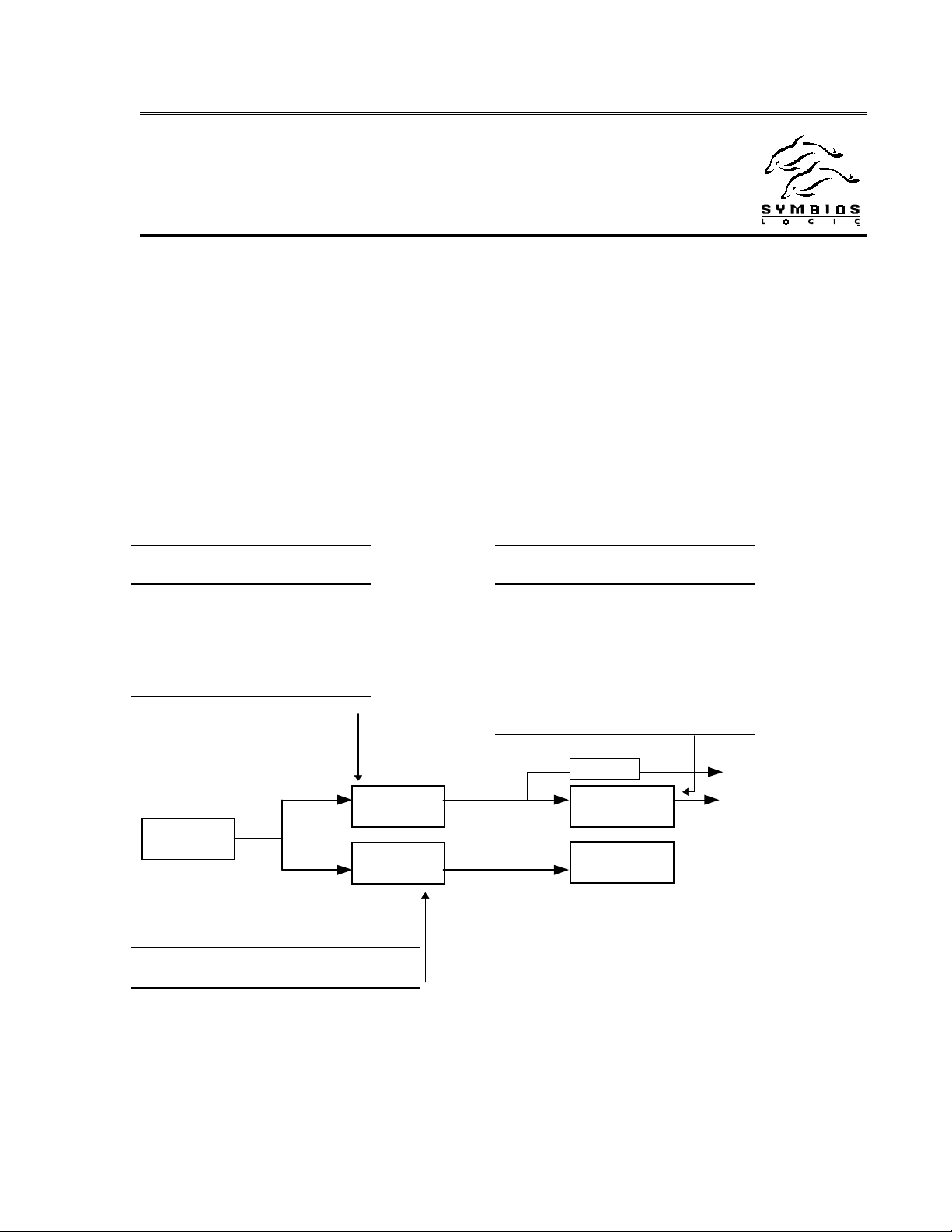
Figure 2-4, “Determining the Synchronous Transfer Rate,” was inadvertently omitted. See the
reference to this figure under the main heading “Synchronous Operation.” The
below.
drawing appears
SCF2 SCF1 SCF0 SCF
Divisor
001 1
0 1 0 1.5
011 2
100 3
000 3
SCF
Divider
SCLK
CCF
Divider
CF2 CCF1 CCF0 SCSI Clock
(MHz)
0 0 0 50.1-66.00
0 0 1 16.67-25.00
0 1 0 25.01-37.50
0 1 1 37.51-50.00
1 0 0 50.01-66.00
This point
must not
exceed 50
MHz
TP2 TP1 TP0 XFERP
Divisor
000 4
001 5
010 6
011 7
100 8
101 9
11010
11111
Divide by 4
Synchronous
Divider
Asynchronous
SCSI Logic
Receive
Clock
Send Clock
(to SCSI bus)
Example:
SCLK= 40 MHz, SCF = 1(/1), XFERP = 0(/4),
CCF = 3(37.51-50.00MHz)
Synchronous send rate = (SCLK/SCF)/XFERP =
(40/1)/4=10MB/s
Synchronous receive rate = (SCLK/SCF)/4 =
(40/1)/4=10MB/s
Figure 2-4: Determining the Synchronous Transfer
Rate
1
Page 2

Achieving Optimal SCSI Send Rates
In this section on page 2-11, the example at the end of the paragraph is incomplete. The TP and
SCF bit settings given in the example will achieve a synchronous send rate of 5 MB/s.
Power Management
The SYM53C810AE complies with the PCI Bus Power Management Interface Specification,
Revision 1.0. The PCI Function Power States are defined in that specification: D0, D1, D2, and
D3. D0 and D3 are required by specification and D1 and D2 are optional. D0 is the maximum
powered state, and D3 is the minimum powered state. Power state D3 is further categorized as
D3hot or D3cold. A function that is powered off is said to be in the D3cold power state.
The power states for the SCSI function are independently controlled through two power state bits
that are located in the PCI Configuration Space Register 44h. The bits are encoded as: 00b –
power state D0, 01b - reserved, 10b - reserved, and 11b - power state D3.
The power states--D0 and D3--are described below. Power states D1 and D2 are not implemented
for this device.
Power State D0
Power state D0 is the maximum power state and is the power-up default state for each function.
Power State D3
Power state D3 is the minimum power state, which includes subsettings called D3hot and
D3cold. The devices are considered to be in power state D3cold when power is removed from
them. D3cold can transition to D0 by applying Vcc and resetting the device. D3hot allows the
device to transition to D0 via software. To obtain power reduction in D3hot, the SCSI clock and
the SCSI clock doubler Phase Lock Loop (PLL) are disabled. Furthermore, soft reset is
continually asserted while in power state D3hot, which clears all pending interrupts and tristates
the SCSI bus. In addition, the function’s PCI command register is cleared.
2
Page 3

Chapter 3, PCI Functional Description
Configuration Registers
Figure 3-1
31 16 15 0
Note:
: PCI Configuration Register Map
Device ID Vendor ID = 1000h 00h
Status Command 04h
Class Code Rev ID 08h
Not Supported Header Type Latency Timer Cache Line Size 0Ch
Base Address Zero (I/O), SCSI Operating Registers 10h
Base Address One (Memory), SCSI Operating Registers 14h
Base Address Two (Memory) SCRIPTS RAM 18h
Not Supported 1Ch
Not Supported 20h
Not Supported 24h
Reserved 28h
Subsystem ID Subsystem Vendor ID 2Ch
Expansion ROM Base Address 30h
Reserved Capabilities Pointer 34h
Reserved 38h
Max_Lat Min_Gnt Interrupt Pin Interrupt Line 3Ch
Power Management Capabilities Next Item Pointer Capability ID 40h
Data Bridge Support Ext Pwr. Mgmt. Control/Status Register 44h
Shaded areas are reserved or represent the SYM53C810AE capabilities.
3
Page 4

Configuration Register Changes
for
SYM53C810AE
Register 2Ch
Subsystem Vendor ID (SSVID)
Read Only
SVID SVID SVID SVID
15-12 11-8 7-4 3-0
Default>>>
1 0 0 0
This register supports subsystem identification, which has a default value of 1000h in the
SYM53C810AE.
Register 2Eh
Subsystem ID (SSID)
Read Only
SID SID SID SID
15-12 11-8 7-4 3-0
Default>>>
1 0 0 0
This register supports subsystem identification, which has a default value of 1000h in the
SYM53C810AE.
Register 06h
Status
Read/Write
DPE SSE RMA RTA RES DT DPR RES NC RES
15 14 13 12 11 10-9 8 7-5 4 3-0
Default >>>
00
00000010
Reads to this register behave normally. Writes are slightly different in that bits can be cleared,
but not set. A bit is reset whenever the register is written and the data in the corresponding bit
location is a one. For instance, to clear bit 15 and not affect any other bits, write the value 8000h
to the register.
Please note the following changes to Register 06h bits 7-0.
Bits 7-5 Reserved
Bit 4 New Capabilities (NC)
This bit is set to indicate the presence of a list of extended capabilities such as PCI Power
Management. This bit is Read Only.
Bits 3-0 Reserved
4
Page 5

Register 08h
Revision ID
Read Only
RID RID RID RID RID RID RID RID
76543210
Default >>>
00
100011
This field specifies device and revision identifiers. The value of this register is
23h.
Register 34h
Capability Pointer
Read Only
CP CP CP CP CP CP CP CP
76543210
Default >>>
01
000000
This register provides an offset into the function’s PCI Configuration Space for the location of
the first item in the capabilities linked list. This register is set by the device to 40h.
Register 40h
Capability ID
Read Only
CID CID CID CID CID CID CID CID
76543210
Default >>>
00
000001
This register indicates the type of the current data structure (linked list item). This register is set
by the device to a value of 01h, indicating the Power Management Data Structure.
Register 41h
Next Item Pointer
Read Only
NP NP NP NP NP NP NP NP
76543210
Default >>>
00
000000
This register describes the location of the next item in the function’s capability list. This register
is set by the device to a value of 00h, indicating that power management is the last capability in
the linked list of extended capabilities.
5
Page 6

Register 42h
Power Management Capabilities
Read Only
PMES D2S D1S RES DSI APS PMEC VER
15-11 10 9 8-6 5 4 3 2-0
Default >>>
00
000001
This register indicates the power management capabilities.
Bits 15-11 PME Support (PMES)
This field always returns a zero value because the devices do not provide a PME signal.
Bit 10 D2 Support (D2S)
This device does not support the D2 power management state.
Bit 9 D1 Support (D1S)
This device does not support the D1 power management state.
Bits 8-6 Reserved
Bit 5 Device Specific Initialization (DSI)
This bit is set to 0 to indicate that the device requires no special initialization before the generic
class device driver is able to use it.
Bit 4 Auxiliary Power Source (APS)
Because the device does not provide a PME signal, this bit always returns a 0. This indicates that
no auxiliary power source is required to support the PME signal in the D3cold power
management state.
Bit 3 PME Clock (PMEC)
This bit always returns a 0b value because the SYM53C810AE does not provide a PME signal.
Bits 2-0 Version (VER)
This field is set to 001b to indicate that the device complies with Revision 1.0 of the PCI Power
Management Interface Specification.
Register 44h
Power Management Control/Status
Read/Write
PST DSCL DSLT PEN RES PWS
15 14-13 12-9 8 7-2 1-0
Default >>>
00
0000
This register indicates the power management control and status descriptions.
6
Page 7

Bit 15 PME Status (PST)
The device always returns a 0 for this bit, indicating that PME signal generation is not supported from D3cold.
Bits 14-13 Data Scale (DSCL)
The device does not support the Data register, therefore this field is always set to 00b.
Bits 12-9 Data Select (DSLT)
The device does not support the Data register, therefore this field is always set to 0000b
.
Bit 8 PME Enable (PEN)
The device always returns a 0 for this bit to indicate that PME assertion is disabled.
Bits 7-2 Reserved
Bits 1-0 Power State (PWS)
This two bit field determines the current power state for the function and is used to set the
function to a new power state. The definitions of the field values are:
00b - D0
01b - Reserved
10b - Reserved
11b - D3hot
Register 46h
PMCSR BSE
Read Only
BSE BSE BSE BSE BSE BSE BSE BSE
76543210
Default >>>
00
000000
This register can support PCI bridge specific functionality if required. The default value always
returns 00h.
Register 47h
Data
Read Only
This register provides an optional mechanism for the function to report state-dependent operating
data. The default value is 00h.
This is currently not implemented for these devices.
7
Page 8

Chapter 5, Operating Registers
On page 5-12, the formula given to calculate the synchronous send and receive rates is incorrect.
The correct formula is:
Synchronous Send Rate = (SCLK/SCF)/XFERP
Synchronous Receive Rate = (SCLK/SCF)/4
Key:
SCLK = SCSI Clock
SCF = Synchronous Clock Conversion Factor, SCNTL3 bits 6-4
XFERP = Transfer period, SXFER register bits 7-5
8
 Loading...