

Page 1

TECHNICAL
MANUAL
LSI53C320
Ultra320 SCSI
Bus Expander
Version 2.2
September 2003
®
DB14-000163-05
Page 2

LSI Logic products are not intended for use in life-support appliances, devices,
or systems. Use of any LSI Logic product in such applications without written
consent of the appropriate LSI Logic officer is prohibited.
Document DB14-000163-05, September 2003
This document describes the LSI Logic LSI53C320 Ultra320 SCSI Bus Expander
and will remain the official reference source for all revisions/releases of this
product until rescinded by an update.
LSI Logic Corporation reserves the right to make changes to any products herein
at any time without notice. LSI Logic does not assume any responsibility or
liability arising out of the application or use of any product described herein,
except as expressly agreed to in writing by LSI Logic; nor does the purchase or
use of a product from LSI Logic convey a license under any patent rights,
copyrights, trademark rights, or any other of the intellectual property rights of
LSI Logic or third parties.
Copyright © 2003 by LSI Logic Corporation. All rights reserved.
TRADEMARK ACKNOWLEDGMENT
LSI Logic, the LSI Logic logo design, LVDlink, SureLINK, and TolerANT are
trademarks or registered trademarks of LSI Logic Corporation. All other brand
and product names may be trademarks of their respective companies.
To receive product literature, visit us at http://www.lsilogic.com.
For a current list of our distributors, sales offices, and design resource
centers, view our web page located at
http://www.lsilogic.com/contacts/index.html
KL
ii
Version 2.2 Copyright © 2003 by LSI Logic Corporation. All rights reserved.
Page 3

Audience
Preface
This manual provides a description of the LSI53C320 Ultra320 SCSI Bus
Expander chip that supports all combinations of Single-Ended (SE) and
Low Voltage Differential (LVD) SCSI bus conversions.
This manual assumes prior knowledge of the current and proposed SCSI
standards. This manual also assumes that you are familiar with
microprocessors and related support devices. The people who benefit
from this book are
• engineers and/or managers who are evaluating the LSI53C320 for
use in a system
• engineers who are designing the LSI53C320 into a system.
Related Publications
For background information, please contact:
LSI Logic World Wide Web Home Page
ANSI
www.ansi.org
Global Engineering Documents
www.global.ihs.com
Ask for document number X3.131-1994 (SCSI-2) or X3.253
(SCSI-3 Parallel Interface)
LSI53C320 Ultra320 SCSI Bus Expander Technical Manual iii
Version 2.2 Copyright © 2003 by LSI Logic Corporation. All rights reserved.
www.lsilogic.com
Page 4
Organization
ENDL Publications
www.rahul.net/endl/
(408) 867-6630
Document names: SCSI Bench Reference, SCSI Encyclopedia, SCSI
Tutor
This document has the following chapters and appendixes:
• Chapter 1, Introduction, contains the general information about the
LSI53C320 product.
• Chapter 2, Functional Descriptions, describes the block diagram
and operation of the LSI53C320.
• Chapter 3, Signal Description, provides signal descriptions for the
LSI53C320.
• Chapter 4, Specifications, contains the electrical characteristics,
timing diagrams, 272-PBGA diagram, and mechanical drawings for
the LSI53C320.
• Appendix A, Wiring Diagrams, contains wiring diagrams for a typical
LSI53C320 usage.
• Appendix B, Glossary, defines commonly used terms.
Revision Record
Date Version Remarks
2/2001 1.0 Advance/Confidential - includes 272 PBGA mechanical drawing
9/2002 1.1 Rearranged Chapters 2-3 into Chapters 2-4.
5/2003 2.0 Final Version for GCA.
5/2003 2.1 Added disclaimer on the EPBGA mechanical drawing.
9/2003 2.2 Added ground to address lines in Figure 2.5 and Figure A.1.
iv Preface
Updated the Specifications chapter for G12 processes.
Rewrote in active voice.
Added the serial EEPROM interface information.
Added the maximum cable length information.
Noted that QAS is not supported in the Ultra160 SCSI mode.
Version 2.2 Copyright © 2003 by LSI Logic Corporation. All rights reserved.
Page 5

Contents
Chapter 1 Introduction
1.1 General Description 1-1
1.2 Applications 1-3
1.3 Benefits of Ultra320 SCSI 1-5
1.4 Benefits of SureLINK™ (Ultra320 SCSI Domain Validation) 1-6
1.5 Benefits of LVDlink™ Technology 1-6
1.6 Benefits of TolerANT®Technology 1-7
1.7 Features 1-7
Chapter 2 Functional Descriptions
2.1 LSI53C320 Block Diagram Description 2-1
2.1.1 SCSI Control Blocks 2-2
2.1.2 Retiming Logic Block 2-2
2.1.3 Precision Delay Control Block 2-3
2.1.4 State Machine Control Block 2-3
2.1.5 DIFFSENS Receiver Block 2-3
2.2 Ultra320 SCSI Functional Description 2-3
2.2.1 Ultra320 SCSI Features 2-3
2.2.2 SCSI Bus Interface 2-7
2.2.3 Maximum Cable Lengths 2-8
2.3 SCSI Signal Processing 2-11
2.3.1 Data and Data Parity Signals 2-11
2.3.2 Select Signal 2-11
2.3.3 Busy Signal 2-12
2.3.4 Reset Signal 2-12
2.3.5 Request and Acknowledge Signals 2-13
2.3.6 Control/Data, Input/Output, Message, and Attention
Signals 2-14
2.4 Internal Control Descriptions 2-14
Contents v
Version 2.2 Copyright © 2003 by LSI Logic Corporation. All rights reserved.
Page 6

2.4.1 Self-Calibration 2-14
2.4.2 Delay Line Structures 2-14
2.4.3 Busy Filters 2-15
2.5 Serial EEPROM Connection 2-15
Chapter 3 Signal Description
3.1 Signal Grouping 3-1
3.2 SCSI Interface Signals 3-3
3.3 Interface Control Signals 3-5
3.4 Serial EEPROM Signals 3-6
3.5 Power and Ground Signals 3-6
3.6 Test Signals 3-7
3.7 Signal Layout Considerations 3-8
Chapter 4 Specifications
4.1 Electrical Characteristics 4-1
4.1.1 DC Characteristics 4-1
4.1.2 TolerANT Technology Electrical Characteristics 4-6
4.1.3 AC Characteristics 4-7
4.2 Chip Drawings 4-8
4.2.1 Mechanical Drawing 4-8
4.2.2 BGA Drawing 4-11
Appendix A Wiring Diagrams
A.1 LSI53C320 Wiring Diagrams A-1
Appendix B Glossary
Index
Customer Feedback
vi Contents
Version 2.2 Copyright © 2003 by LSI Logic Corporation. All rights reserved.
Page 7

Figures
1.1 LSI53C320 SCSI Bus Modes 1-2
1.2 LSI53C320 Server Clustering 1-3
1.3 LSI53C320 SCSI Bus Device 1-4
2.1 LSI53C320 Block Diagram 2-2
2.2 Paced Transfer Example 2-5
2.3 Example of Precompensation 2-6
2.4 Electrical Cable Lengths at Ultra320 SCSI Speeds 2-10
2.5 Serial EEPROM Connection 2-16
3.1 LSI53C320 Functional Signal Grouping 3-2
4.1 LVD Driver 4-3
4.2 LVD Receiver 4-3
4.3 Rise and Fall Time Test Conditions 4-7
4.4 Clock Timing 4-8
4.5 272-Ball-Count PBGA (VG) Mechanical Drawing 4-9
4.6 LSI53C320 272-Ball BGA Top View 4-12
A.1 LSI53C320 Wiring Diagram 1 of 4 A-2
A.2 LSI53C320 Wiring Diagram 2 of 4 A-3
A.3 LSI53C320 Wiring Diagram 3 of 4 A-4
A.4 LSI53C320 Wiring Diagram 4 of 4 A-5
Contents vii
Version 2.2 Copyright © 2003 by LSI Logic Corporation. All rights reserved.
Page 8

viii Contents
Version 2.2 Copyright © 2003 by LSI Logic Corporation. All rights reserved.
Page 9

Tables
1.1 Types of Operation 1-2
1.2 SCSI Bus Length Limits in a Clustering Configuration 1-4
1.3 SCSI Bus Length Limits 1-5
2.1 DIFFSENS Voltage Levels 2-8
2.2 Total Cable Length for Ultra320 SCSI Using the
LSI53C320 2-10
3.1 SCSI A Side Interface Signals 3-3
3.2 SCSI B Side Interface Signals 3-4
3.3 Chip Interface Control Signals 3-5
3.4 Serial EEPROM Signals 3-6
3.5 Power and Ground Pins 3-6
3.6 Test Signals for LSI Logic Only 3-7
4.1 Absolute Maximum Stress Ratings 4-1
4.2 Operating Conditions 4-2
4.3 LVD Driver SCSI Signals—SD[15:0]±, SDP[1:0]±,
SCD±, SIO±, SMSG±, SREQ±,SACK±, SBSY±,
SATN±, SSEL±, SRST± 4-2
4.4 LVD Receiver SCSI Signals—SD[15:0]±, SDP[1:0]±,
SCD±, SIO±, SMSG±, SREQ±,SACK±, SBSY±,
SATN±, SSEL±, SRST± 4-3
4.5 Bidirectional SCSI Signals—SD[15:0]/, SDP[1:0]/, SREQ/,
SACK/, SD[15:0]±, SDP[1:0]±, SREQ±,SACK± 4-4
4.6 Bidirectional SCSI Control Signals—SCD/, SIO/, SMSG/,
SBSY/, SATN/, SSEL/, SRST/, SCD±, SIO±, SMSG±,
SBSY±,SATN±, SSEL±, SRST± 4-4
4.7 DIFFSENS SCSI Signal 4-4
4.8 Input Capacitance 4-5
4.9 Input Control Signals—CLOCK, CHIP_RESET/,
WS_ENABLE/ 4-5
4.10 Output Control Signals—BSY_LED, XFER_ACTIVE 4-5
4.11 TolerANT Technology Electrical Characteristics 4-6
4.12 Clock Timing 4-8
Contents ix
Version 2.2 Copyright © 2003 by LSI Logic Corporation. All rights reserved.
Page 10

x Contents
Version 2.2 Copyright © 2003 by LSI Logic Corporation. All rights reserved.
Page 11

Chapter 1
Introduction
This chapter describes the LSI53C320 Ultra320 SCSI Bus Expander and
includes these sections:
• Section 1.1, “General Description,” page 1-1
• Section 1.2, “Applications,” page 1-3
• Section 1.3, “Benefits of Ultra320 SCSI,” page 1-5
• Section 1.4, “Benefits of SureLINK™ (Ultra320 SCSI Domain
Validation),” page 1-6
• Section 1.5, “Benefits of LVDlink™ Technology,” page 1-6
• Section 1.6, “Benefits of TolerANT
• Section 1.7, “Features,” page 1-7
®
Technology,” page 1-7
1.1 General Description
The LSI53C320 Ultra320 SCSI Bus Expander is a single-chip solution
allowing the extension of SCSI device connectivity and/or cable length
limits. A SCSI bus expander couples bus segments without impact to the
software, firmware, or SCSI protocol implementation. The LSI53C320
Ultra320 SCSI Bus Expander connects Single-Ended (SE) Ultra SCSI
and Low Voltage Differential (LVD) Ultra320 SCSI peripherals together in
any combination. The LSI53C320 does not support High Voltage
Differential (HVD) mode.
The LSI53C320 supports any combination of the SE or LVD bus modes
on either the A Side or B Side port. This provides the system designer
with maximum flexibility in designing SCSI backplanes to accommodate
any SCSI bus mode. Each bus side on the LSI53C320 has an
independent RBIAS pin to allow for margining of each bus.
LSI53C320 Ultra320 SCSI Bus Expander Technical Manual 1-1
Version 2.2 Copyright © 2003 by LSI Logic Corporation. All rights reserved.
Page 12

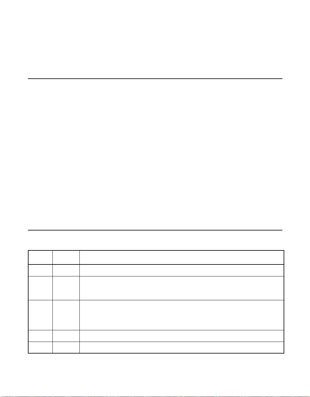
Figure 1.1 shows the two SCSI bus modes available on the A or B Side.
LVDlink transceivers provide the multimode LVD or SE capability. The
LSI53C320 operates as both an expander and a converter. In both SCSI
Bus Expander and Converter modes, the LSI53C320 isolates the cable
segments on the A Side and the B Side. This feature maintains the signal
integrity of each cable segment.
Figure 1.1 LSI53C320 SCSI Bus Modes
A Side B Side
LVD
SE
LSI53C320
SCSI Expander
LVD
SE
Table 1.1 shows the types of operational modes for the LSI53C320.
Table 1.1 Types of Operation
Signal Type Speed
LVD to LVD Up to Ultra320 SCSI
SE to SE Up to Ultra SCSI
LVD to SE Up to Ultra SCSI
SE to LVD Up to Ultra SCSI
The LSI53C320 provides additional control capability through the pinlevel isolation mode (Warm Swap Enable). This feature permits logical
disconnection of the A Side bus or the B Side bus without disrupting
SCSI transfers currently in progress. For example, users can logically
disconnect the B Side bus while the A Side bus remains active.
The LSI53C320 is based on proven LSI Logic bus expander technology,
which includes signal filtering along with retiming to maintain skew
budgets. The LSI53C320 is independent of software. However, Domain
Validation technology does require software control.
Note: The LSI53C320 does not support Quick Arbitration and
1-2 Introduction
Version 2.2 Copyright © 2003 by LSI Logic Corporation. All rights reserved.
Selection (QAS) while operating at Ultra160 SCSI rates.
Page 13
1.2 Applications
The LSI53C320 supports
• server clustering environments
• expanders creating distinct SCSI cable segments that are isolated
Configurations that use the LSI53C320 SCSI Bus Expander in the LVD
to LVD mode allow the system designer to take advantage of the inherent
cable distance, device connectivity, data reliability, and increased transfer
rate benefits of LVD signaling with Ultra320 SCSI peripherals. Section
2.2.3, “Maximum Cable Lengths,” discusses additional limits on the total
SCSI cable length for systems operating at Ultra320 SCSI transfer rates.
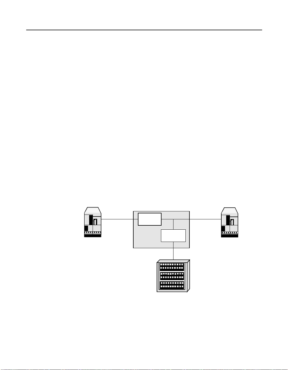
Figure 1.2 shows how SCSI bus expanders couple bus segments with no
impact on the SCSI protocol or software. Two LSI53C320 expanders
configure three bus segments. Segment A is a point-to-point segment.
Segments B and C are load segments and have at least 8 inches
between every node. Table 1.2 shows the various distance requirements
for each SCSI bus segment.
Figure 1.2 LSI53C320 Server Clustering
from each other
Segment A
Primary Server
Applications 1-3
Version 2.2 Copyright © 2003 by LSI Logic Corporation. All rights reserved.
SCSI Bus
Expander
SCSI Bus
Expander
Segment C
Shared Disk Subsystem
Segment B
Secondary Server
Page 14
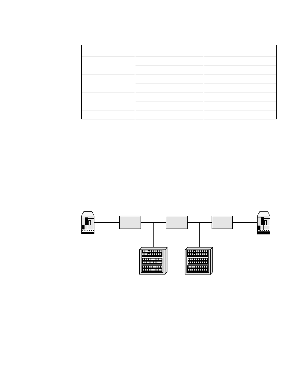
Table 1.2 SCSI Bus Length Limits in a Clustering Configuration
Segment Mode Length Limit
A LVD (Ultra320 SCSI) Up to 12 meters
SE (Ultra SCSI) Up to 3 meters
1
B LVD (Ultra320 SCSI) Up to 12 meters
SE (Ultra SCSI) Up to 1.5 meters
C LVD (Ultra320 SCSI) Up to 12 meters
SE (Ultra SCSI) Up to 1.5 meters
A + B + C + D Ultra320 SCSI (only) Less than 29 meters
2
1. The cable length can be more than 1.5 meters, since this is a point-to-point
connection.
2. Refer to Section 2.2.3, “Maximum Cable Lengths,” for more information on
cable length limits in an Ultra320 SCSI environment.
Figure 1.3 shows cascading of the LSI53C320 to achieve four distinct
SCSI segments. Segments A and D are point-to-point segments.
Segments B and C are load segments and have at least 8-inch spacing
between every node. Table 1.3 shows the distance requirements for each
SCSI bus segment.
Figure 1.3 LSI53C320 SCSI Bus Device
Segment A Segment B Segment C
Primary
Server
1-4 Introduction
Version 2.2 Copyright © 2003 by LSI Logic Corporation. All rights reserved.
SCSI Bus
Expander
Shared Disk
Subsystem
SCSI Bus
Expander
Shared Disk
Subsystem
SCSI Bus
Expander
Segment D
Secondary
Server
Page 15
Table 1.3 SCSI Bus Length Limits
Segment Mode Length Limit
A, D LVD (Ultra320 SCSI) Up to 12 meters
SE (Ultra SCSI) Up to 1.5 meters
B, C LVD (Ultra320 SCSI) Up to 12 meters
SE (Ultra SCSI) Up to 1.5 meters
A + B + C + D Ultra320 SCSI (only) Less than 25 meters
1. Refer to Section 2.2.3, “Maximum Cable Lengths,” for more information on
cable length limits in an Ultra320 SCSI environment.
1.3 Benefits of Ultra320 SCSI
The LSI53C320 SCSI Bus Expander supports Ultra320 SCSI. This
interface expands the bandwidth of the SCSI bus to allow faster
synchronous data transfers of up to 320 Mbytes/s. Ultra320 SCSI
provides double the data transfer rate of the Ultra160 SCSI interface.
The LSI53C320 performs 16-bit, Ultra320 SCSI synchronous data
transfers as fast as 320 Mbytes/s on the side of the device. This
advantage is most noticeable in heavily loaded systems or large block
size applications, such as video on-demand and image processing.
1
Ultra320 SCSI doubles both the data and clock frequencies from
Ultra160 SCSI. Due to the increased data and clock speeds, Ultra320
SCSI introduces skew compensation and intersymbol interference (ISI)
compensation. These new features simplify system design by resolving
timing issues at the chip level. Skew compensation adjusts for timing
differences between data and clock signals caused by cabling, board
traces, and so on. ISI compensation enhances the first pulse after a
change in state to ensure data integrity. The LSI53C320 performs skew
compensation on the receiver side of the device and ISI compensation
on the driver side of the device.
Ultra320 SCSI supports Cyclic Redundancy Check (CRC), which
provides error checking code to detect the validity of data. CRC
increases the reliability of data transfers by transferring four bytes of
code along with data. CRC detects all single bit errors, two bits in error,
or other error types within a single 32-bit range.
Benefits of Ultra320 SCSI 1-5
Version 2.2 Copyright © 2003 by LSI Logic Corporation. All rights reserved.
Page 16

1.4 Benefits of SureLINK™ (Ultra320 SCSI Domain Validation)
SureLINK Domain Validation is a procedure that allows a host computer
and target SCSI peripheral to negotiate and find the optimal transfer
speed. This procedure improves overall reliability of the system by
ensuring data integrity.
Domain Validation software ensures robust SCSI interconnect
management and low risk Ultra320 SCSI implementations by extending
the domain validation guidelines documented in the SPI-4 specifications.
Domain validation verifies that the system is capable of transferring data
at Ultra320 SCSI speeds, allowing the LSI53C320 to renegotiate to a
lower data transfer speed and bus width if necessary. SureLINK Domain
Validation is the software control for the domain validation manageability
enhancements in the LSI53C320. SureLINK Domain Validation software
provides domain validation management at boot time as well as during
system operation.
SureLINK Domain Validationensures robust system operation by providing
three levelsof integrity checking on a per-device basis: Basic (Lev el1) with
inquiry command; Enhanced (Level2) with read/write buffer; and Margined
(Level 3) with margining of drive strength and slew rates.
1.5 Benefits of LVDlink™ Technology
The LSI53C320 supports LVDlink technology for SCSI, a signaling
technology that increases the reliability of SCSI data transfers over
longer distances than those supported by SE SCSI technology. The low
current output of LVD allows the I/O transceivers to be integrated directly
onto the chip. For backward compatibility to existing SE devices, the
LSI53C320 features multimode LVDlink transceivers that can switch
between LVD and SE modes.
Some features of integrated LVDlink transceivers are listed below:
• supports SE or LVD modes
• allows greater device connectivity and longer cable length
• saves the cost of external differential transceivers
• provides a long-term performance migration path
1-6 Introduction
Version 2.2 Copyright © 2003 by LSI Logic Corporation. All rights reserved.
Page 17

1.6 Benefits of TolerANT®Technology
The LSI53C1320 features TolerANT technology, which provides active
negation on the SCSI drivers and input signal filtering on the SCSI
receivers. Active negation causes the SCSI Request, Acknowledge,
Data, and Parity signals to be actively driven HIGH rather than passively
pulled up by terminators.
TolerANT receiver technology improves data integrity in unreliable
cabling environments where other devices would be subject to data
corruption. TolerANT receivers filter the SCSI bus signals to eliminate
unwanted transitions, without the long signal delay associated with
RC-type input filters. This improved driver and receiver technology helps
ensure correct clocking of data.
TolerANT technology increases noise immunity, balances duty cycles,
and improves SCSI transfer rates. In addition, TolerANT SCSI devices do
not cause glitches on the SCSI bus at power-up or power-down, which
protects other devices on the bus from data corruption. When used with
the LVDlink transceivers, TolerANT technology provides excellent signal
quality and data reliability in real world cabling environments.
1.7 Features
The LSI53C320
• complies with the SCSI Parallel Interface 4 (SPI-4) Specifications
– complies with SCSI Enhanced Parallel Interface (EPI)
Specifications
– supports Double Transition (DT) clocking
– supports CRC in DT data phases
– supports Domain Validation technology
– supports Ultra320 SCSI Packetized Transfers
– provides SCSI signal and timing calibration
– is backward-compatible with previous revisions of the SCSI
specification
Benefits of TolerANT®Technology 1-7
Version 2.2 Copyright © 2003 by LSI Logic Corporation. All rights reserved.
Page 18

• provides a flexible SCSI bus expander
• supports any combination of LVD or SE transceivers
• creates distinct SCSI bus segments that are isolated from each other
• uses integrated LVDlink transceivers for direct attachment to either
LVD or SE bus segments
• operates as a SCSI Bus Expander or a SCSI Bus Converter
– LVD to LVD (Ultra320 SCSI or Ultra160 SCSI)
– SE to SE (up to Ultra SCSI)
– LVD to SE (up to Ultra SCSI)
– SE to LVD (up to Ultra SCSI)
• handles targets and initiators on either the A Side bus or B Side bus
• accepts any asynchronous or synchronous transfer speeds up to
Ultra320 SCSI (for LVD to LVD mode only)
• supports dynamic addition/removal of SCSI bus segments using the
isolation mode
• does not consume a SCSI ID
• propagates the RESET/ signal from one side to the other regardless
of the SCSI bus state
• notifies initiator(s) of changes in transmission mode (SE/LVD) on A
or B Side segments by using the SCSI bus RESET/
• provides a SCSI Busy LED driver for an activity indicator
• supports cascading of up to four LSI53C320s
• does not require software
• requires a 40 MHz Input Clock
• has a 272-pin Plastic Ball Grid Array package (PBGA).
1-8 Introduction
Version 2.2 Copyright © 2003 by LSI Logic Corporation. All rights reserved.
Page 19

Chapter 2
Functional
Descriptions
This chapter describes all signals, their groupings, and their functions. It
includes these topics:
• Section 2.1, “LSI53C320 Block Diagram Description,” page 2-1
• Section 2.2, “Ultra320 SCSI Functional Description,” page 2-3
• Section 2.3, “SCSI Signal Processing,” page 2-11
• Section 2.4, “Internal Control Descriptions,” page 2-14
• Section 2.5, “Serial EEPROM Connection,” page 2-15
2.1 LSI53C320 Block Diagram Description
The LSI53C320 has no user programmable registers and does not
require software. SCSI control signals control all LSI53C320 functions.
Figure 2.1 shows a block diagram of the LSI53C320 device, which
consists of these specific areas:
• A Side SCSI Control Block
– LVD and SE Drivers and Receivers
• B Side SCSI Control Block
– LVD and SE Drivers and Receivers
• Retiming Logic
• Precision Delay Control
• State Machine Control
LSI53C320 Ultra320 SCSI Bus Expander Technical Manual 2-1
Version 2.2 Copyright © 2003 by LSI Logic Corporation. All rights reserved.
Page 20
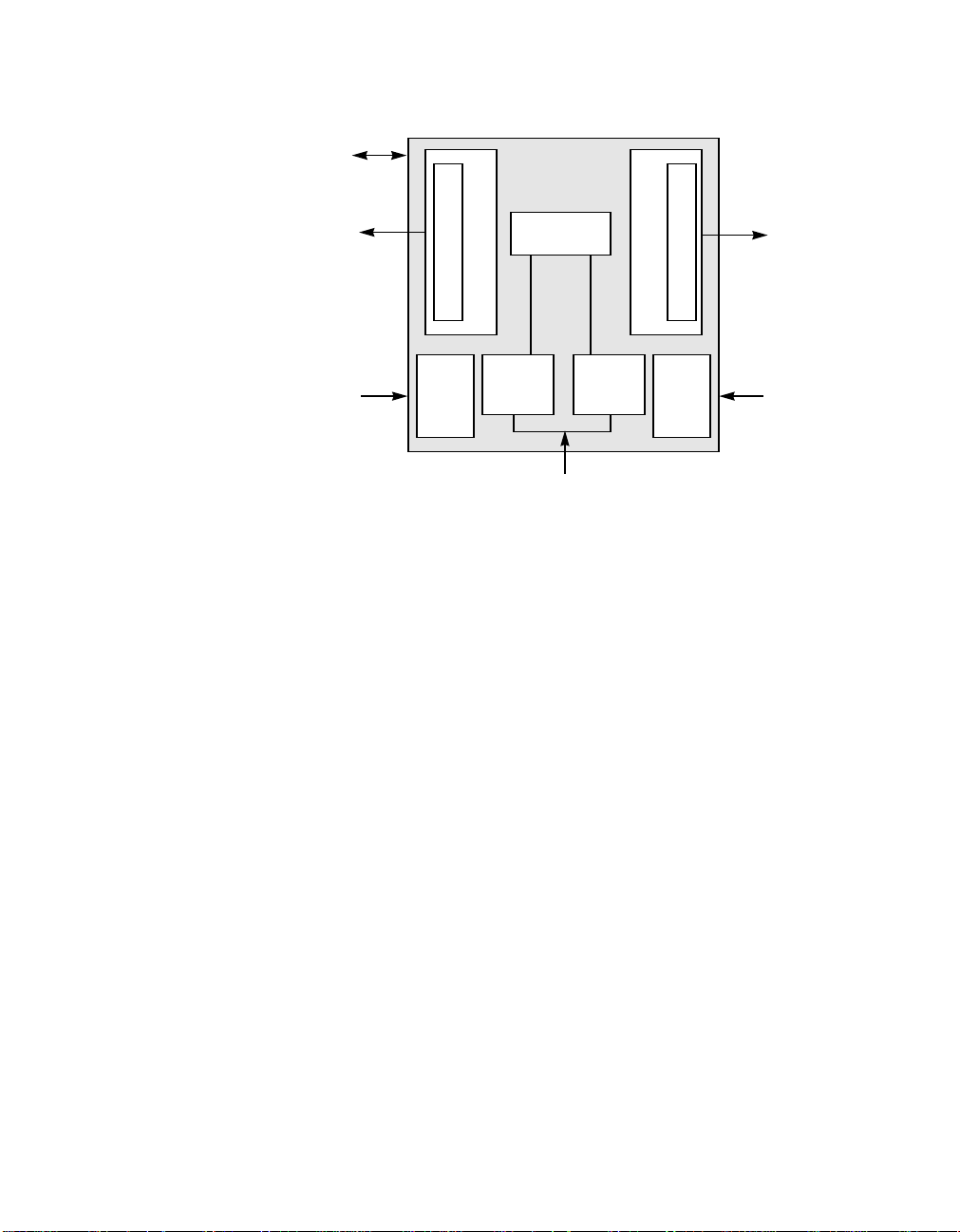
Figure 2.1 LSI53C320 Block Diagram
Control
Signals
k
A Side Signals
A_DIFFSENS B_DIFFSENS
The LSI53C320 passes data and parity from a source bus to a load bus.
The source bus receives the SCSI signals from the initiator. The load bus
transmits the SCSI signals to the target. The LSI53C320 retimes signals
to maintain the signal skew budget from the source bus to the load bus.
2.1.1 SCSI Control Blocks
The SCSI A Side pins internally connect to the corresponding SCSI B
Side pins. In the LVD/LVD mode, the A Side and B Side control blocks
connect to SCSI devices and accept any asynchronous or synchronous
Ultra320 SCSI data transfer rates. The SCSI control block supports
TolerANT and LVDlink technologies to enable the SCSI bus transfers.
For more information on these technologies, refer to Section 2.2.2.1,
“SCSI Bus Modes.”
ansceivers
VDlink Tr
L
er
VD
L
Receiv
DIFFSENS
Retiming
ol Block
SCSI Contr
Logic
Precision
Delay
Control
40 MHz Clock Input
State
Machine
Control
ol Bloc
LVDlink Transceivers
SCSI Contr
LVD
Receiver
DIFFSENS
B Side Signals
2.1.2 Retiming Logic Block
As SCSI signals propagate through the LSI53C320, the chip retimes the
signals to improve the SCSI timing. The Retiming Logic block contains
numerous delay elements, which the Precision Delay Control block
periodically calibrates to guarantee the output pulse widths, setup times,
and hold times.
2-2 Functional Descriptions
Version 2.2 Copyright © 2003 by LSI Logic Corporation. All rights reserved.
Page 21

A synchronous negotiation between devices forms a nexus, for which the
on-chip RAM stores information. This information remains in place until
a chip reset, power down, or renegotiation. The nexus information
enables the LSI53C320 to make accurate retiming adjustments.
2.1.3 Precision Delay Control Block
The Precision Delay Control block provides calibration information to the
precision delay elements in the Retiming Logic block. Since the
LSI53C320 voltage and temperature vary with time, the Precision Delay
Control block periodically updates the delay settings in the Retiming
Logic block to maintain constant and precise control over the bus timing.
2.1.4 State Machine Control Block
The State Machine Control block monitors the SCSI bus phases, the
initiator and target device IDs, and various timing functions. This block
controls the SCSI bus signal retiming and SCSI protocol implementation.
2.1.5 DIFFSENS Receiver Block
The LSI53C320 can operate with SE or LVD SCSI buses. The
DIFFSENS Receiver block determine the operating mode of the SCSI
bus by monitoring the voltage level on the DIFFSENS signal. For more
information, refer to Section 2.2.2.1, “SCSI Bus Modes.”
2.2 Ultra320 SCSI Functional Description
The LSI53C320 supports Ultra320 SCSI. This interface expands the
bandwidth of the SCSI bus to allow faster synchronous data transfers of
up to 320 Mbytes/s. Ultra320 SCSI doubles the data transfer rate as
compared to the Ultra160 SCSI interface. This section describes how the
LSI53C320 implements the features in the SPI-4 draft specification.
2.2.1 Ultra320 SCSI Features
This section describes the Ultra320 SCSI features in the LSI53C320.
Ultra320 SCSI Functional Description 2-3
Version 2.2 Copyright © 2003 by LSI Logic Corporation. All rights reserved.
Page 22

2.2.1.1 Double Transition (DT) Clocking
Ultra160 SCSI and Ultra320 SCSI implement DT clocking to provide
speeds up to 80 megatransfers per second (megatransfers/s) for
Ultra160 SCSI, and up to 160 megatransfers/s for Ultra320 SCSI. When
implementing DT clocking, a SCSI device samples data on both the
asserting and deasserting edge of REQ/ACK. DT clocking is only valid
using an LVD SCSI bus.
2.2.1.2 Intersymbol Interference (ISI) Compensation
ISI Compensation uses paced transfers and precompensation to enable
high data transfer rates. Ultra320 SCSI data transfers require the use of
ISI Compensation.
Paced Transfers – The initiator and target must establish a paced
transfer agreement that specifies the REQ/ACK offset and the transfer
period before using this feature. Devices can only perform paced
transfers during Ultra320 SCSI DT data phases. In paced transfers, the
device sourcing the data drives the REQ/ACK signal as a free running
clock. The transition of the REQ/ACK signal, either the assertion or the
negation, clocks data across the bus. For successful completion of a
paced transfer, the number of ACK transitions must equal the number of
REQ transitions, and both the REQ and ACK lines must be negated.
The P1 line indicates valid data in 4-byte quantities by using its phase.
The transmitting device indicates the start of valid data state by holding
the state of the P1 line for the first two data transfer periods. Beginning
on the third data transfer period, the transmitting device continues the
valid data state by toggling the state of the P1 line every two data
transfer periods for as long as the data is valid. The transmitting device
must toggle the P1 line coincident with the REQ/ACK assertion. This
method provides a minimum valid data period of two transfer periods.
To pause the data transfer, the transmitting device reverses the phase of
P1 by withholding the next transition of P1 at the start of the first two
invalid data transfer periods. Beginning with the third invalid data transfer
period, the transmitting device toggles the P1 line every two invalid data
transfer periods until it sends valid data. The transmitting device returns
to the valid data state by reversing the phase of the P1 line. The invalid
data state must experience at least one P1 transition before returning to
2-4 Functional Descriptions
Version 2.2 Copyright © 2003 by LSI Logic Corporation. All rights reserved.
Page 23
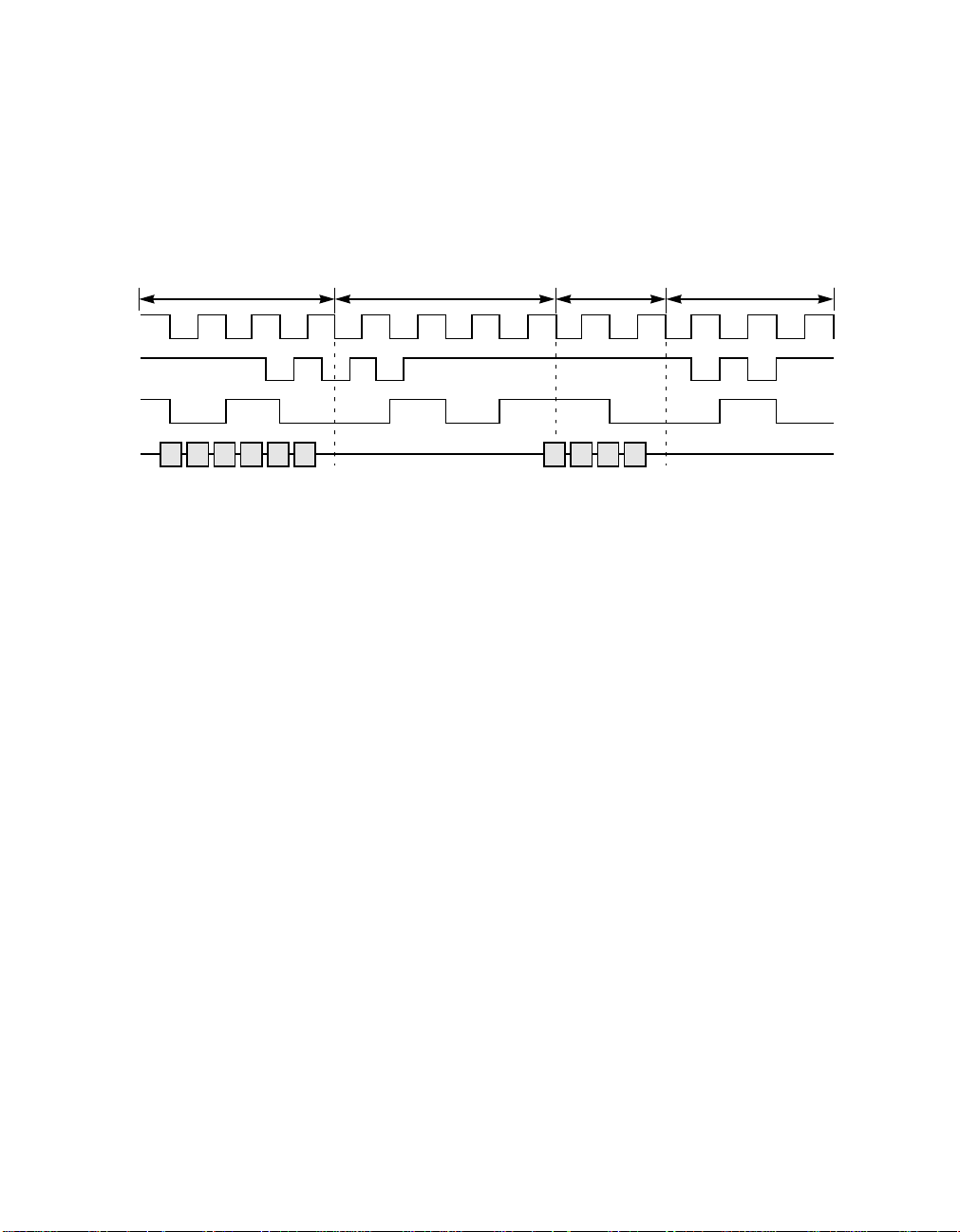
the valid data state. This method provides a minimum invalid data period
of four transfer periods.
Figure 2.2 provides a waveform diagram of paced data transfers and
illustrates the use of the P1 line.
Figure 2.2 Paced Transfer Example
Invalid DataValid Data Valid Data Invalid Data
REQ
ACK
P1
DATA
The LSI53C320 uses the PPR negotiation that the SPI-4 draft standard
describes to establish a paced transfer agreement with the initiator on
the source bus and the target on the load bus.
Precompensation – When transmitting in the Ultra320 SCSI mode, the
LSI53C320 can use precompensation to adjust the strength of the REQ,
ACK, parity, and data signals. When a signal transitions to HIGH or LOW,
the LSI53C320 drives the signal at the signal drive strength for the first
data transfer period, and then lowers the signal drive strength on the
second data transfer period if the signal remains in the same state. The
LSI53C320 maintains the lower signal drive strength until the signal
again transitions HIGH or LOW. Figure 2.3 illustrates the drivers
performance with precompensation enabled and disabled.
Ultra320 SCSI Functional Description 2-5
Version 2.2 Copyright © 2003 by LSI Logic Corporation. All rights reserved.
Page 24

Figure 2.3 Example of Precompensation
a. Drivers with Precompensation Disabled
Normal Drive Strength
b. Drivers with Precompensation Enabled
Normal Drive Strength
2.2.1.3 Packetized Transfers
Packetized transfers are also referred to as information unit transfers.
They reduce overhead on the SCSI bus by merging several of the SCSI
bus phases.
2.2.1.4 Skew Compensation
The LSI53C320 provides a method to account for and control system
skew between the clock and data signals. Skew compensation is only
available when the device operates in the Ultra320 SCSI mode. The
initiator-target pair uses the training sequences in the SPI-4 draft
standard to determine the skew compensation. The LSI53C320 passes
the training patterns between the initiator and target. The LSI53C320
stores the adjustment parameters and recalls them on subsequent
connections with the given device pair (nexus).
Reduced Drive Strength
2-6 Functional Descriptions
Version 2.2 Copyright © 2003 by LSI Logic Corporation. All rights reserved.
Page 25

2.2.1.5 Cyclic Redundancy Check (CRC)
Ultra320 SCSI and Ultra160 SCSI devices employ CRC as an error
detection code during the DT Data phases. The LSI53C320 handles
CRC as another data phase with the appropriate specific timing values.
2.2.1.6 LSI53C320 Requirements for Synchronous SCSI Negotiation
The LSI53C320 builds a table of information regarding devices on the
bus in on-chip RAM. The LSI53C320 reads the PPR, Synchronous Data
Transfer Request (SDTR), and Wide Data Transfer Request (WDTR)
information for each device from the MSG bytes during negotiation.
For devices to communicate accurately through the LSI53C320 at
Ultra320 SCSI rates, it is necessary for a complete asynchronous
negotiation to occur between the initiator and target(s) prior to any
synchronous data transfer. The LSI53C320 defaults to Ultra SCSI rates
when a valid negotiation between the initiator and target does not occur.
2.2.2 SCSI Bus Interface
This section describes the SCSI bus interfaces on the LSI53C320.
2.2.2.1 SCSI Bus Modes
To support greater device connectivity and longer SCSI cables, the
LSI53C320 features LVDlink technology, the LSI Logic implementation of
multimode LVD SCSI. The LVDlink transceivers can operate in the LVD
or SE modes.
The voltage levels on the A_DIFFSENS and B_DIFFSENS signals
determine the SCSI bus mode. The LSI53C320 DIFFSENS receivers
detect the voltage level on the A Side or B Side DIFFSENS lines
independently. The LSI53C320 does not change the present signal mode
until it continuously senses a new DIFFSENS voltage level for 100 ms.
Table 2.1 shows the voltages on the DIFFSENS lines.
Ultra320 SCSI Functional Description 2-7
Version 2.2 Copyright © 2003 by LSI Logic Corporation. All rights reserved.
Page 26

Table 2.1 DIFFSENS Voltage Levels
Mode Voltage
SE −0.35 to +0.5
LVD +0.7 to +1.9
When the DIFFSENS voltage selects SE mode, the LSI53C230 internally
ties the plus signals to ground and the minus SCSI signals become the
SE input/outputs. When the DIFFSENS voltage selects LVD mode, the
plus and minus signals are the differential signal pairs.
Any dynamic mode change (SE-to-LVD or LVD-to-SE) on a bus segment
is a significant event, and the initiator must determine if the new bus
mode meets the requirements for the bus segment. The LSI53C320
supports dynamic transmission mode changes by notifying the initiator(s)
of changes in the transmission mode with a SCSI bus RESET/. The
DIFFSENS line detects a valid mode switch on a bus segment. After the
DIFFSENS state is continuously present for 100 ms, the LSI53C320
generates a SCSI reset on the bus opposite the bus on which the
transmission mode change occurred. This reset informs initiators residing
on the opposite bus segment of the change in the transmission mode.
The initiator(s) then renegotiates synchronous transfer rates with each
device on that segment.
If the LSI53C320 detects the HVD mode on a SCSI bus segment, the
LSI53C320 3-states its outputs.
2.2.2.2 SCSI Termination
The terminator networks pull signals to an inactive voltage level and
match the impedance seen at the end of the cable with the characteristic
impedance of the cable. Install terminators at the ends of each SCSI
segment, and only at the ends; all SCSI buses must have exactly two
terminators.
2.2.3 Maximum Cable Lengths
The electrical length of a bus is the time required for round-trip signal
propagation between bus ends. This section discusses the maximum
electrical and physical cable lengths when cascading LSI53C320
2-8 Functional Descriptions
Version 2.2 Copyright © 2003 by LSI Logic Corporation. All rights reserved.
Page 27

expanders. For Ultra320 SCSI environments, the information in this
section takes precedence over the information in Section 1.2,
“Applications.”
2.2.3.1 Maximum Electrical Cable Length
The SCSI Parallel Interface-4 (SPI-4) standard states that the electrical
length between the hosts arbitrating on different ends of a SCSI bus
must not exceed 800 nanoseconds (ns), when operating at Ultra320
SCSI data transfer rates. Due to this constraint, LSI Logic specifies that
a maximum of four expanders can be cascaded on a SCSI bus.
There are additional electrical length constraints imposed by the SPI-4
standard. When ending a paced transfer from DT
the target must wait 800 ns before issuing a REQ. The SPI-4 standards
allows 200 ns for the host to recognize the phase change and stop the
free running ACK. This requirement reduces the electrical length of the
bus to 600 ns.
Because the expander resides in the middle of the bus and retimes data
to the active free running clock, the expander must switch its internal
logic from ACK to REQ. The expander performs this switch 600 ns after
detecting the phase change. Activity on the ACK or REQ line during this
period adversely affects the expander. This reduces the electrical length
of the bus to 400 ns.
to any other phase,
OUT
Figure 2.4 illustrates the bus timing. Assuming a 400 ns electrical length
and that the host uses the full 200 ns time allotment, the last free running
ACK from the host returns to the expander at the 600 ns mark.
Ultra320 SCSI Functional Description 2-9
Version 2.2 Copyright © 2003 by LSI Logic Corporation. All rights reserved.
Page 28

Figure 2.4 Electrical Cable Lengths at Ultra320 SCSI Speeds
800 ns from the phase change to the first REQ of the new phase
600 ns: Requirement for expander
200 ns:
Phase change
delay to the host
200 ns:
Host delay to stop
free-running ACKS
200 ns:
Delay until the last ACK
arrives at the LSI53C320
2.2.3.2 Maximum Physical Cable Length
Table 2.2 provides information concerning the maximum physical cable
length when operating the LSI53C320 at Ultra320 SCSI transfer rates.
Table 2.2 Total Cable Length for Ultra320 SCSI Using the LSI53C320
Number of Cascaded
Expanders
1 37
2 29
3 25
4 21
Maximum Physical Cable
Length in Meters (m)
Comments
LSI Logic recommends limiting the 25 m
point-to-point bus cable length to 20 m and
the fully-loaded bus cable length to 12 m.
The SPI-4 standard allows a maximum point-to-point physical cable
length of 25 m and a maximum fully loaded physical cable length 12 m.
This limits the total physical cable length to 37 m. To allow for board
capacitance and signal propagation through the expander, LSI Logic
recommends limiting the point-to-point physical cable length to 20 m.
This limits the total physical cable length to 32 m.
Table 2.2 provides the total maximum cable length depending on the
number of expanders that are cascaded on the bus. As long as the total
cable length between expanders, hosts, and drives does not exceed
these limits, the 400 ns electrical cable length requirement will be met.
2-10 Functional Descriptions
Version 2.2 Copyright © 2003 by LSI Logic Corporation. All rights reserved.
Page 29

In designs that use a back plane, designers must additionally consider
the signal propagation velocity through the back plane to ensure that the
400 ns electrical cable length requirement is met.
2.3 SCSI Signal Processing
Figure 3.1 shows the LSI53C320 signal grouping. The following sections
describes the signal processing for the LSI53C320 SCSI signals. Refer
to Section Chapter 3, “Signal Description,” and Section Chapter 4,
“Specifications,” for more information on individual signals.
2.3.1 Data and Data Parity Signals
The LSI53C320 passes the data and parity signals from the source bus
to the load bus and provides the necessary edge shifting to guarantee
the skew budget for the load bus. Either side of the LSI53C320 can act
as the source bus or the load bus. The side that the LSI53C320 receives
signals on is the source bus. The side that the LSI53C320 drives signals
on is the load bus. These steps describe the LSI53C320 data
processing:
1. The receiver logic accepts the data. Once the clock signal
(REQ/ACK) is received, the LSI53C320 gates the data from the
receiver latch.
2. The LSI53C320 holds the asserting edge for a specified time to
3. The LSI53C320 samples the bus using a latch, which provides a
4. In the last stage, the LSI53C320 3-states the outputs.
5. To assure that the LSI53C320 does not sample its own signals, the
2.3.2 Select Signal
A_SSEL and B_SSEL perform bus arbitration and selection. When a bus
asserts the SSEL signal, the LSI53C320 propagates the signal assertion
SCSI Signal Processing 2-11
Version 2.2 Copyright © 2003 by LSI Logic Corporation. All rights reserved.
prevent signal bounce. The input signal controls the duration of the
hold time.
stable data window for the load bus.
LSI53C320 delays sampling until a specified time after the last signal
deassertion.
Page 30

to the other bus. When both buses assert SSEL simultaneously, A_SSEL
takes precedence over B_SSEL. The SSEL output has a pull-down
control for an open collector driver. The following steps describe the
select control signal process:
1. If the LSI53C320 is driving the SSEL signal, the LSI53C320 blocks
2. The LSI53C320 filters the leading edge of the SSEL signal to ensure
3. To assure that the LSI53C320 does not sample its own signals, the
2.3.3 Busy Signal
The controller propagates the A_SBSY and B_SBSY signals from the
source bus to the load bus. The following steps describe the busy control
signal process:
1. The LSI53C320 filters the leading edge of the SBSY signal. The
the SSEL input signal on the other bus.
that the output does not switch for a specified time after the leading
edge. The duration of the input signal determines the duration of the
output signal.
LSI53C320 delays sampling until a specified time after the last signal
deassertion.
LSI53C320 holds the assertion edge for a specified time to prevent
signal bounce. The duration of the input signal determines the
duration of the output signal.
2. To assure that the LSI53C320 does not sample its own signals, the
LSI53C320 delays sampling until a specified time after the last signal
deassertion.
2.3.4 Reset Signal
The controller passes the A_SRST and B_SRST signals from the source
to the load bus. This output has pull-down control for an open collector
driver. The following steps describe the processing of the reset signals:
1. If the LSI53C320 is driving the SRST signal, the LSI53C320 blocks
the SRST input signal on the other bus.
2. The LSI53C320 filters the leading edge of the signal to ensure that
the output does not switch during a specified time after the leading
2-12 Functional Descriptions
Version 2.2 Copyright © 2003 by LSI Logic Corporation. All rights reserved.
Page 31

edge. The duration of the input signal determines the duration of the
output signal.
3. To assure that the LSI53C320 does not sample its own signals, the
LSI53C320 delays sampling until a specified time after the last signal
deassertion.
2.3.5 Request and Acknowledge Signals
The SREQ and SACK signal paths contain controls that guarantee
minimum pulse widths, filter edges, and perform signal retiming.
When performing DT clocking, the LSI53C320 filters both the leading and
trailing signal edges. When performing ST clocking, the LSI53C320 filters
only the leading signal edge. The SREQ and SACK paths are from the
A Side to the B Side and from the B Side to the A Side. The following
steps describe the SREQ and SACK signal processing:
1. The LSI53C320 senses the asserted input signal and forwards it to
the next stage if the direction control permits. The LSI53C320 state
machine develops the direction controls from the sequence of the
bus control signals.
2. The LSI53C320 filters the leading edge of the input and output signal
to ensure that the signal does not switch during the specified hold
time after the leading edge. The duration of the input signal
determines the duration of the output signal after the hold time. The
LSI53C320 guarantees a minimum pulse width.
3. The LSI53C320 passes the signal to the load bus if the signal is not
a data clock. If SREQ or SACK is a data clock, it delays the leading
edge to improve data output setup times. The duration of the input
signal determines the duration of the output signal.
4. The LSI53C320 filters the trailing edge of the signal to prevent signal
bounce after the signal deasserts. The LSI53C320 deasserts the
output signal at the first deasserted edge of the input signal.
5. In the last stage, the LSI53C320 3-states the outputs.
6. To assure that the LSI53C320 does not sample its own signals, the
LSI53C320 delays sampling until a specified time after the last signal
deassertion.
SCSI Signal Processing 2-13
Version 2.2 Copyright © 2003 by LSI Logic Corporation. All rights reserved.
Page 32

2.3.6 Control/Data, Input/Output, Message, and Attention Signals
The following steps describe the processing of these signals:
1. If the LSI53C320 is driving the signal, the LSI53C320 blocks the
input signal on the other bus.
2. The LSI53C320 filters the leading edge of the signal to ensure that
the output does not switch for a specified time after the leading edge.
The duration of the input signal determines the duration of the output
signal.
3. In the last stage, the LSI53C320 3-states the outputs.
4. To assure that the LSI53C320 does not sample its own signals, the
LSI53C320 delays sampling until a specified time after the last signal
deassertion.
2.4 Internal Control Descriptions
This section provides information about self-calibration, delay line
structures, and busy filters.
2.4.1 Self-Calibration
The LSI53C320 triggers self-calibration to adjust for variations in
temperature, process, and voltage every second during bus free states.
2.4.2 Delay Line Structures
The signal and control interfaces for bus to bus transfers require fixed
delay functions. The LSI53C320 uses programmable delay lines to
implement the delay functions. Multiplexers select the incremental points
in the delay chain. The LSI53C320 self-calibration manages the effects
of temperature and voltage changes.
2.4.2.1 Data Path
The data path through the LSI53C320 includes two levels of latches. The
first latch in the data path is located in the receiver and the REQ/ACK
input clock and generates a hold. This latch holds the received data to
capture incoming data that might have minimal setup and hold times. A
2-14 Functional Descriptions
Version 2.2 Copyright © 2003 by LSI Logic Corporation. All rights reserved.
Page 33

second latch is located on the transmitter side of the LSI53C320 and
holds the data to enable optimal signal transmission on the isolated bus.
This latch provides a regenerated clock signal and the maximum setup
and hold times.
The data path also provides a timer for each data bit. This timer protects
against reception from a target bus for a nominal 30 ns after the driver
deasserts.
2.4.2.2 REQ/ACK Retiming
The LSI53C320 edge filters the REQ/ACK input clock signals. The chip
also stretches these signals to their minimum timing values to avoid
glitches. In double transition clocking, the chip filters both the leading and
trailing edges. In single transition clocking, the chip filters only the
leading edge. The filters remove noise within the initial signal transition.
The current transmission speed determines the filter time values.
2.4.3 Busy Filters
The busy control signal passes from source to load bus. The current
state of the SCSI bus determines the filtering. This filter provides a
synchronized leading edge signal that is not true until the input signal
stabilizes. The trailing edge occurs within several nanoseconds of the
input deasserting. When the BSY signal asserts before and after the SEL
signal, the filter is on.
2.5 Serial EEPROM Connection
The serial EEPROM connects to the LSI53C320 through a 2-wire serial
interface. SP_CLK (Ball C7) on the LSI53C320 connects to the serial
EEPROM clock line and SP_DAT (Ball B6) on the LSI53C320 connects
to the serial EEPROM data line. These two lines are pulled HIGH
through resistors.
The LSI53C320 produces the 50 kHz SP_CLK for downloading data from
the serial EEPROM. The LSI53C320 3-states the SP_CLK and SP_DAT
lines during chip reset and after a successful download. The LSI53C320
continues to drive SP_CLK LOW if the download is unsuccessful, which
enables detection of download failure by monitoring this signal.
Serial EEPROM Connection 2-15
Version 2.2 Copyright © 2003 by LSI Logic Corporation. All rights reserved.
Page 34

LSI Logic recommends using a 3.3 V, 2 Kbyte (256 x 8 bit) serial
EEPROM that can accept a 50 KHz clock. Figure 2.5 provides a sample
layout.
Figure 2.5 Serial EEPROM Connection
3.3 V
1.0 µF
10%
3.3 V
4.75 KΩ
10%
VCC
A2
A1
A0
WP
Serial EEPROM
(24C16)
3.3 V 3.3 V
CLK
DAT
4.75 KΩ
10%
4.75 KΩ
10%
C7
B6
LSI53C320
S_CLK
S_DATA
2-16 Functional Descriptions
Version 2.2 Copyright © 2003 by LSI Logic Corporation. All rights reserved.
Page 35

Chapter 3
Signal Description
This chapter provides the signal descriptions and electrical
characteristics for the LSI53C320. It includes these topics:
• Section 3.1, “Signal Grouping,” page 3-1
• Section 3.2, “SCSI Interface Signals,” page 3-3
• Section 3.3, “Interface Control Signals,” page 3-5
• Section 3.4, “Serial EEPROM Signals,” page 3-6
• Section 3.5, “Power and Ground Signals,” page 3-6
• Section 3.6, “Test Signals,” page 3-7
• Section 3.7, “Signal Layout Considerations,” page 3-8
3.1 Signal Grouping
Figure 3.1 illustrates the LSI53C320 signal grouping.
LSI53C320 Ultra320 SCSI Bus Expander Technical Manual 3-1
Version 2.2 Copyright © 2003 by LSI Logic Corporation. All rights reserved.
Page 36

Figure 3.1 LSI53C320 Functional Signal Grouping
A Side
LVD or SE
SCSI Interface
Control
Signals
A_SSEL+
A_SSELA_SBSY+
A_SBSYA_SRST+
A_SRSTA_SREQ+
A_SREQA_SACK+
A_SACKA_SMSG+
A_SMSGA_SCD+
A_SCDA_SIO+
A_SIOA_SATN+
A_SATNA_SDP[1:0]+
A_SDP[1:0]A_SD[15:0]+
A_SD[15:0]-
A_DIFFSENS
A_RBIAS
CHIP_RESET/
WS_ENABLE/
XFER_ACTIVE
CLOCK
BSY_LED
LSI53C320
B_SSEL+
B_SSEL-
B_SBSY+
B_SBSY-
B_SRST+
B_SRST-
B_SREQ+
B_SREQ-
B_SACK+
B_SACK-
B_SMSG+
B_SMSG-
B_SCD+
B_SCD-
B_SIO+
B_SIO-
B_SATN+
B_SATN-
B_SDP[1:0]+
B_SDP[1:0]-
B_SD[15:0]+
B_SD[15:0]-
B_DIFFSENS
B_RBIAS
S_SLC
S_DATA
B Side
LVD or SE
SCSI Interface
Serial
EEPROM
Signals
3-2 Signal Description
Version 2.2 Copyright © 2003 by LSI Logic Corporation. All rights reserved.
Page 37

3.2 SCSI Interface Signals
Table 3.1 describes the SCSI interface signals for the A Side of the
LSI53C320.
Table 3.1 SCSI A Side Interface Signals
Signal Name BGA Pin Type Description
A_SSEL+
A_SSEL-
A_SBSY+
A_SBSY-
A_SRST+
A_SRST-
A_SREQ+
A_SREQ-
A_SACK+
A_SACK-
A_SMSG+
A_SMSG-
A_SCD+
A_SCD-
A_SIO+
A_SIO-
A_SATN+
A_SATN-
A_SDP[1:0]+
A_SDP[1:0]-
A_SD[15:0]+
G1
H3
K3
K1
J3
J2
F2
F1
J1
K2
H2
H1
G3
G2
E1
F3
L2
L3
V2, M1
W1, M2
W3, W4, Y3, V5, B1, D2, C1, E3,
N1, N3, P2, P3, T1, T2, T3, V1,
I/O A Side Select signal.
I/O A Side Busy signal.
I/O A Side Reset signal.
I/O A Side Request signal.
I/O A Side Acknowledge signal.
I/O A Side Message signal.
I/O A Side Control and Data signal.
I/O A Side Input and Output signal.
I/O A Side Attention signal.
I/O A Side Data Parity signals.
I/O A Side Data signals.
A_SD[15:0]-
A_DIFFSENS B3 I A Side Differential Sense signal.
A_RBIAS M3 RBIAS A Side current control. Attach a
Y2, V4, Y4, W5, C2, D3, D1, E2,
N2, P1, R1, R2, R3, U1, U2, U3
10 kΩ pull-up resistor on RBIAS
to provide the correct bias level.
SCSI Interface Signals 3-3
Version 2.2 Copyright © 2003 by LSI Logic Corporation. All rights reserved.
Page 38

Table 3.2 describes the SCSI interface signals for the B Side of the
LSI53C320.
Table 3.2 SCSI B Side Interface Signals
Signal Name Pin Type Description
B_SSEL+
B_SSEL-
B_SBSY+
B_SBSY-
B_SRST+
B_SRST-
B_SREQ+
B_SREQ-
B_SACK+
B_SACK-
B_SMSG+
B_SMSG-
B_SCD+
B_SCD-
B_SIO+
B_SIO-
B_SATN+
B_SATN-
B_SDP[1:0]+
B_SDP[1:0]−
B_SD[15:0]+,
H19
H18
F18
E19
F20
G18
J20
J19
F19
E20
G20
G19
J18
H20
K19
K18
D20
E18
A14, D19
C13, C20
B13, C12, A12, C11, N19, M18,
M20, L18, C19, A19, B17, A18,
C16, A16, B15, C14
I/O B Side Select signal.
I/O B Side Busy signal.
I/O B Side Reset signal.
I/O B Side Request signal.
I/O B Side Acknowledge signal.
I/O B Side Message signal.
I/O B Side Control and Data signal.
I/O B Side Input and Output signal.
I/O B Side Attention signal.
I/O B Side Data Parity signals.
I/O B Side Data signals.
B_SD[15:0]−
B_DIFFSENS B2 I B Side Differential Sense signal.
B_RBIAS D18 RBIAS LVD current control. Attach a 10
3-4 Signal Description
A13, B12, B11, A11, N20, M19,
L19, L20, B20, B18, C17, A17,
B16, C15, A15, B14
kΩ pull-up resistor on RBIAS to
provide the correct bias level.
Version 2.2 Copyright © 2003 by LSI Logic Corporation. All rights reserved.
Page 39

3.3 Interface Control Signals
Table 3.3 describes the interface control signals for the LSI53C320. The
LSI53C320 requires an external POR, which is implemented using the
CHIP_RESET/ signal. Figure A.1 provides an example external POR
circuit.
Table 3.3 Chip Interface Control Signals
Signal Name Pin Type Description
CHIP_RESET/ C10 I The active LOW Master Reset signal provides a general purpose
WS_ENABLE/ A7 I TheActive LOW Warm Swap Enable signal enables and disables
XFER_ACTIVE A8 O The Transfer Active signal enables and disables SCSI transfers
CLOCK A9 I CLOCK provides the 40 MHz oscillator input to the LSI53C320. It
BSY_LED B9 O The Busy LED signal provides an 8 mA SCSI activity LED output.
chip reset that forces the internal elements of the LSI53C320 to a
known state. Asserting this signal places the LSI53C320 state
machine in an idle state and places all controls in a passive state.
The minimum CHIP_RESET/ asserted pulse width is 100 ns.
SCSI transfers through the LSI53C320. The WS_ENABLE/ input
removes the chip from an active bus without disturbing the current
SCSI transaction. When Warm Swap Enable asserts, the
LSI53C320 3-states the SCSI signals after it detects the next bus
free state. The LSI53C320 no longer passes on signals until the
WS_ENABLE/ pin deasserts and both SCSI buses enter the Bus
Free state.
through the LSI53C320. The LSI53C320 asserts this signal when
the chip is active to indicate that the chip completed its internal
testing, the SCSI bus has entered a bus free state, or that SCSI
traffic can now pass from one side of the chip to the other side of
the chip. The LSI53C320 deasserts this signal to detect a Bus
Free state due to the WS_ENABLE/ signal being LOW.
Deasserting this signal disables transfers through the device.
is the clock source for the protocol control state machines and
timing generation logic. The bus signal transfer paths do not use
this clock.
The LSI53C320 asserts this signal to indicate SCSI bus activity.
Interface Control Signals 3-5
Version 2.2 Copyright © 2003 by LSI Logic Corporation. All rights reserved.
Page 40

3.4 Serial EEPROM Signals
Table 3.4 describes the serial EEPROM signals for the LSI53C320.
Table 3.4 Serial EEPROM Signals
Signal Name Pin Type Description
S_CLK C7 O The LSI53C320 uses the serial EEPROM clock signal to provide
the 50 kHz clock for downloading the serial EEPROM data.
S_DATA B6 I/O The LSI53C320 uses the serial EEPROM data signal to
download data from the serial EEPROM.
3.5 Power and Ground Signals
Table 3.5 describes the power and ground signals for the LSI53C320.
Table 3.5 Power and Ground Pins
Signal Name Pin Type Description
SCSI
CORE
3, 4
IO
SCSI
CORE
IO
1
D6, D11, D15, F4, F17, K4, L17, R4, R17,
U6, U10, U15
2
A2, B19, D10, K17, L4, U11, W2, W19 I Power supplies to the CORE
I Power supplies to the SCSI bus
I/O pins.
logic.
C8 I Power supplies to the I/O logic.
A1, D4, D8, D13, D17, H4, H17, J9, J10,
I Ground ring.
J11, J12, K9, K10, K11, K12, L9, L10, L11,
L12, M9, M10, M11, M12, N4, N17, U4,
U8, U13, U17
4
A20, B10, C3, K20, L1, Y1, Y11, Y20 I Ground ring.
B7 I Ground ring.
VDD
VDD
VDD
VSS
VSS
VSS
3-6 Signal Description
Version 2.2 Copyright © 2003 by LSI Logic Corporation. All rights reserved.
Page 41

Table 3.5 Power and Ground Pins (Cont.)
Signal Name Pin Type Description
NC A3, A5, A6, A10, B8, C4, C6, C9, C18, D5,
D7, D9, D12, D14, D16, E4, E17, G4,
G17, J4, J17, M4, M17, N18, P4, P17,
P18, P19, P20, R18, R19, R20, T4, T17,
T18, T19, T20, U5, U7, U9, U12, U14,
U16, U18, U19, U20, V3, V6, V7, V8, V9,
V10, V11, V12, V13, V14, V15, V16, V17,
V18, V19, V20, W6, W7, W8, W9, W10,
W11, W12, W13, W14, W15, W16, W17,
W18, W20, Y5, Y6, Y7, Y8, Y9, Y10, Y12,
Y13, Y14, Y15, Y16, Y17, Y18, Y19
1. VDD
2. VDD
3. VDD
4. The VDD
must be supplied with 3.3 V.
SCSI
pins must be supplied 1.8 V.
CORE
must be supplied with 3.3 V.
IO
pin must always power down before the VDD
IO
3.6 Test Signals
Table 3.6 lists the LSI53C320 test signals and their associated ball
number. These test signals are for use by LSI Logic only.
Note: Connect the tests signals to either test point or a header for
debugging purposes.
N/A No Connections.
pin.
CORE
Table 3.6 Test Signals for LSI Logic Only
Signal Ball
TEST_3 A4
TEST_4 C5
TEST_5 B5
TEST_6 B4
Test Signals 3-7
Version 2.2 Copyright © 2003 by LSI Logic Corporation. All rights reserved.
Page 42

3.7 Signal Layout Considerations
The pinout of the LSI53C320 package ensures that each signal requires
the shortest possible trace length. Use active termination for the bus
connections to the LSI53C320. When choosing an active terminator, set
the load capacitance of the terminator as low as possible.
LSI Logic recommends the use of strip line. Strip line allows tighter
connector placement, which reduces the noise effects from both internal
and external sources. On long trace runs, such as those in a backplane
environment, snaking of traces to equalize their length is appropriate.
Place the decoupling capacitors as close as possible to the via attached
to each corresponding voltage plane.
3-8 Signal Description
Version 2.2 Copyright © 2003 by LSI Logic Corporation. All rights reserved.
Page 43

Chapter 4
Specifications
This chapter provides the electrical and environmental specifications for
the LSI53C320 and consists of these topics:
• Section 4.1, “Electrical Characteristics,” page 4-1
• Section 4.2, “Chip Drawings,” page 4-8
4.1 Electrical Characteristics
This section provides the electrical characteristics of the LSI53C320.
4.1.1 DC Characteristics
Table 4.1 through 4.10 give the current and voltage specifications.
Figure 4.1 and Figure 4.2 illustrate the driver and receiver schematics.
Table 4.1 Absolute Maximum Stress Ratings
Symbol Parameter Min Max Unit Test Conditions
T
STG
V
DD-Core
V
DD-IO
V
IN
I
LP
ESD Electrostatic Discharge – 2000 V MIL-STD 883C,
1. Stresses beyond those listed can damage the device. These are stress ratings; functional operation
at or beyond these values is not implied.
Storage Temperature –40 125 ˚C –
Supply Voltage –0.3 2.2 V –
IO Supply Voltage −0.3 3.9 V –
Input Voltage −0.5 VDD+ 0.5 V –
Latch-up current ±150 – mA −2V<VPIN<8V
LSI53C320 Ultra320 SCSI Bus Expander Technical Manual 4-1
Version 2.2 Copyright © 2003 by LSI Logic Corporation. All rights reserved.
1
Method 3015.7
Page 44

Table 4.2 Operating Conditions
1
Symbol Parameter Min Nominal Max Unit Test Conditions
V
DD-Core
V
DD-IO
I
DD-Core
I
DD-IO
2
I
LP
T
j
T
A
θ
JA
Supply voltage 1.71 1.80 1.89 V –
I/O Supply voltage 3.13 3.30 3.47
Core and Analog Supply
– 275 360 mA –
Current (Dynamic)
I/O Supply Current
(Dynamic)
– 450 590 mA RBIAS = 10 kΩ 1%
VDD= 3.3 V
Latch-up Current 150 – – mA –
Junction Temperature – 60 115 ˚C –
Operating free air 0 – 70 ˚C –
Thermal resistance
– – 16.4 ˚C/W –
(junction to ambient air)
1. Conditions that exceed the operating limits can cause the device to function incorrectly.
2. SCSI pins only.
Table 4.3 LVD Driver SCSI Signals—SD[15:0]±, SDP[1:0]±, SCD±, SIO±, SMSG±,
SREQ±,SACK±, SBSY±,SATN±, SSEL±, SRST±
1
Symbol Parameter Min Max Units Test Conditions
I
+ Source (+) current 9.6 14.4 mA Asserted state
O
I
− Sink (−) current −9.6 −14.4 mA Asserted state
O
I
+ Source (+) current −6.4 −9.6 mA Negated state
O
I
− Sink (−) current 6.4 9.6 mA Negated state
O
1. V
I
CM
OZ
3-state leakage −20 20 µA–
= 0.7 − 1.8 V, R
bias
=10kΩ.
4-2 Specifications
Version 2.2 Copyright © 2003 by LSI Logic Corporation. All rights reserved.
Page 45

Figure 4.1 LVD Driver
R
L
+
−
IO+
IO−
2
R
L
2
+
V
CM
−
Table 4.4 LVD Receiver SCSI Signals—SD[15:0]±, SDP[1:0]±,
SCD±, SIO±, SMSG±, SREQ±,SACK±, SBSY±,SATN±,
SSEL±, SRST±
1
Symbol Parameter Min Max Units
V
LVD receiver voltage asserting 60 – mV –
I
V
LVD receiver voltage negating – −60 mV –
I
1. VCM= 0.7 − 1.8 V.
Figure 4.2 LVD Receiver
+
V
+
V
CM
−
I
2
−
+
V
I
2
−
+
−
Test
Conditions
Electrical Characteristics 4-3
Version 2.2 Copyright © 2003 by LSI Logic Corporation. All rights reserved.
Page 46
Table 4.5 Bidirectional SCSI Signals—SD[15:0]/, SDP[1:0]/,
SREQ/, SACK/, SD[15:0]±, SDP[1:0]±, SREQ±,SACK±
Symbol Parameter Min Max Unit
V
V
V
OH
V
OL
I
OZ
Input high voltage 1.9 V
IH
Input low voltage V
IL
1
Output high voltage 2.0 V
Output low voltage V
DD
1.0 V –
SS
DD
0.5 V 48 mA
SS
V–
VIOH= 7.0 mA
3-state leakage −10 10 µA–
Conditions
1. TolerANT active negation enabled.
Table 4.6 Bidirectional SCSI Control Signals—SCD/, SIO/, SMSG/,
SBSY/, SATN/, SSEL/, SRST/, SCD±, SIO±, SMSG±,
SBSY±,SATN±, SSEL±, SRST±
Symbol Parameter Min Max Unit Test Conditions
Test
V
V
V
I
OZ
Input high voltage 1.9 V
IH
Input low voltage V
IL
Output low voltage V
OL
DD
1.0 V –
SS
0.5 V 48 mA
SS
V–
3-state leakage −10 10 µA–
Table 4.7 DIFFSENS SCSI Signal
Symbol Parameter Min Max Unit
V
V
I
4-4 Specifications
Version 2.2 Copyright © 2003 by LSI Logic Corporation. All rights reserved.
LVD sense voltage 0.7 1.9 V –
S
Single-ended sense voltage VSS− 0.3 0.5 V –
IL
3-state leakage −10 10 µA–
OZ
Test
Conditions
Page 47

Table 4.8 Input Capacitance
Symbol Parameter Min Max Unit
C
Input capacitance of input pads – 7 pF –
I
C
Input capacitance of I/O pads – 10 pF –
IO
Conditions
Table 4.9 Input Control Signals—CLOCK, CHIP_RESET/,
WS_ENABLE/
Test
Symbol Parameter Min Max Unit Test Conditions
V
V
I
Input high voltage 2.0 V
IH
Input low voltage V
IL
3-state leakage −10 10 µA–
OZ
SS
DD
0.8 V –
V–
Table 4.10 Output Control Signals—BSY_LED, XFER_ACTIVE
Symbol Parameter Min Max Unit Test Conditions
V
V
I
OZ
Output high voltage 2.4 V
OH
Output low voltage V
OL
0.4 V 8 mA
SS
V8mA
DD
3-state leakage −10 10 µA–
Electrical Characteristics 4-5
Version 2.2 Copyright © 2003 by LSI Logic Corporation. All rights reserved.
Page 48

4.1.2 TolerANT Technology Electrical Characteristics
Table 4.11 provides the minimum and maximum values in units for the
TolerANT Technology electrical characteristics.
Table 4.11 TolerANT Technology Electrical Characteristics
Symbol Parameter Min Max Units Test Conditions
1
V
OH
V
OL
V
IH
V
IL
V
IK
V
TH
V
TL
V
TH-VTL
I
OH
I
OL
I
OSH
I
OSL
I
LH
I
LL
R
I
C
P
2
t
R
t
F
dV
H
Output high voltage 2.0 VDD+ 0.3 V IOH=7mA
Output low voltage V
SS
0.5 V IOL=48mA
Input high voltage 2.0 VDD+ 0.3 V –
Input low voltage VSS− 0.3 0.8 V Referenced to V
Input clamp voltage −0.66 −0.77 V VDD= 4.75;
I
= −20 mA
I
Threshold, HIGH to LOW 1.0 1.2 V –
Threshold, LOW to HIGH 1.4 1.6 V –
Hysteresis 300 500 mV –
2
Output high current 2.5 24 mA VOH= 2.5 V
Output low current 100 200 mA VOL= 0.5 V
2
Short-circuit output high current – 625 mA Output driving low, pin
shorted to V
DD
Short-circuit output low current – 95 mA Output driving high, pin
shorted to V
Input high leakage – 20 µA −0.5<VDD<5.25
V
PIN
= 2.7 V
SS
3
Input low leakage – −20 µA −0.5<VDD<5.25
V
= 0.5 V
PIN
Input resistance 20 – MΩ Receivers Disabled
Capacitance per pin – 15 pF PQFP
Rise time, 10% to 90% 4.0 18.5 ns Refer to Figure 4.3
Fall time, 90% to 10% 4.0 18.5 ns Refer to Figure 4.3
/dt Slew rate, LOW to HIGH 0.15 0.50 V/ns Refer to Figure 4.3
SS
supply
supply
3
2
4-6 Specifications
Version 2.2 Copyright © 2003 by LSI Logic Corporation. All rights reserved.
Page 49

Table 4.11 TolerANT Technology Electrical Characteristics (Cont.)
Symbol Parameter Min Max Units Test Conditions
dVL/dt Slew rate, HIGH to LOW 0.15 0.50 V/ns Refer to Figure 4.3
ESD Electrostatic discharge 2 – kV MIL-STD-883C; 3015-7
Latch-up 100 – mA –
Filter delay 20 30 ns –
Ultra filter delay 10 15 ns –
Extended filter delay 40 60 ns –
1. Active negation outputs only: Data, Parity, SREQ/, and SACK/. SCSI SE mode only (minus signals).
2. Single pin only; irreversible damage may occur if sustained for one second.
3. SCSI RESET pin has a 10 kΩ pull-up resistor.
Figure 4.3 Rise and Fall Time Test Conditions
47 Ω
4.1.3 AC Characteristics
The AC characteristics described in this section apply over the entire
range of operating conditions. Chip timing is based on simulation at worst
case voltage, temperature, and processing. The LSI53C320 requires a
40 MHz clock input. Table 4.12 and Figure 4.4 provide clock timing data.
Electrical Characteristics 4-7
Version 2.2 Copyright © 2003 by LSI Logic Corporation. All rights reserved.
20 pF
+
2.5 V
−
Page 50

Table 4.12 Clock Timing
Symbol Parameter Min Max Units
t
1
t
2
t
3
t
4
Figure 4.4 Clock Timing
Clock
4.2 Chip Drawings
This section provides the BGA and mechanical drawings for the
LSI53C320.
4.2.1 Mechanical Drawing
Clock period 24.75 25.25 ns
Clock low time 10 15 ns
Clock high time 10 15 ns
Clock rise time 1 – V/ns
t
1
t
3
t
t
2
4
Figure 4.5 illustrates the LSI53C320 mechanical drawing. The
LSI53C320 uses a 272-ball, PBGA package with a VG package code.
4-8 Specifications
Version 2.2 Copyright © 2003 by LSI Logic Corporation. All rights reserved.
Page 51

Figure 4.5 272-Ball-Count PBGA (VG) Mechanical Drawing (Sheet 1 of 2)
Important: This drawing may not be the latest version. For board layout and manufacturing, obtain
the most recent engineering drawings from your LSI Logic marketing representative by
requesting the outline drawing for package code VG.
Chip Drawings 4-9
Version 2.2 Copyright © 2003 by LSI Logic Corporation. All rights reserved.
Page 52

Figure 4.5 272-Ball-Count PBGA (VG) Mechanical Drawing (Sheet 2 of 2)
Important: This drawing may not be the latest version. For board layout and manufacturing, obtain
the most recent engineering drawings from your LSI Logic marketing representative by
requesting the outline drawing for package code VG.
4-10 Specifications
Version 2.2 Copyright © 2003 by LSI Logic Corporation. All rights reserved.
Page 53

4.2.2 BGA Drawing
Figure 4.6 provides the BGA drawing for the LSI53C320. This drawing
provides the pinout view when looking down on the chip from the top.
Table 4.13 and Table 4.14 provide the pin lists for the LSI53C320.
Chip Drawings 4-11
Version 2.2 Copyright © 2003 by LSI Logic Corporation. All rights reserved.
Page 54

WS_ENABLE/
VSS
IO
NC
1
XFER_ACTIVE
NC BSY_LED
VDD
IO
VSS
SCSI
CLOCK NC
NC
NC
VSS
SCSI
VSS
SCSI
VSS
SCSI
VSS
SCSI
Figure 4.6 LSI53C320 272-Ball BGA Top View
A1 A2 A3 A4 A5 A6 A7 A8 A9 A10
VSS
B1 B2 B3 B4 B5 B6 B7 B8 B9 B10
A_SD11+
C1 C2 C3 C4 C5 C6 C7 C8 C9 C10
A_SD9+ A_SD11-
D1 D2 D3 D4 D5 D6 D7 D8 D9 D10
A_SD9- A_SD10+ A_SD10-
E1 E2 E3 E4
A_SIO+ A_SD8- A_SD8+ NC
F1 F2 F3 F4
A_SREQ- A_SREQ+ A_SIO-
G1 G2 G3 G4
A_SSEL+ A_SCD- A_SCD+ NC
H1 H2 H3 H4
A_SMSG- A_SMSG+ A_SSEL-
J1 J2 J3 J4 J9 J10
A_SACK+ A_SRST- A_SRST+ NC
K1 K2 K3 K4 K9 K10
A_SBSY- A_SACK- A_SBSY+
L1 L2 L3 L4 L9 L10
VSS
M1 M2 M3 M4 M9 M10
A_SDP0+ A_SDP0- A_RBIAS NC
N1 N2 N3 N4
A_SD7+ A_SD7- A_SD6+
P1 P2 P3 P4
VDD
SCSI
CORE
CORE
B_DIFFSENS A_DIFFSENS
A_SATN+ A_SATN-
NC TEST_3 NC NC
TEST_6 TEST_5 S_DATA
VSS
CORE
NC TEST_4 NC S_CLK
VSS
VDD
VSS
VDD
VDD
VSS
SCSI
SCSI
SCSI
SCSI
CORE
SCSI
NC
VDD
SCSI
VSS
CORE
CHIP_RESET/
VDD
CORE
VSS
SCSI
VSS
SCSI
VSS
SCSI
VSS
SCSI
A_SD6- A_SD5+ A_SD4+ NC
R1 R2 R3 R4
A_SD5- A_SD4- A_SD3-
T1 T2 T3 T4
A_SD3+ A_SD2+ A_SD1+ NC
U1 U2 U3 U4 U5 U6 U7 U8 U9 U10
A_SD2- A_SD1- A_SD0-
V1 V2 V3 V4 V5 V6 V7 V8 V9 V10
A_SD0+ A_SDP1+ NC A_SD14- A_SD12+ NC NC NC NC NC
W1 W2 W3 W4 W5 W6 W7 W8 W9 W10
A_SDP1-
Y1 Y2 Y3 Y4 Y5 Y6 Y7 Y8 Y9 Y10
VSS
VDD
A_SD15- A_SD13+ A_SD13- NC NC NC NC NC NC
CORE
A_SD15+ A_SD14+ A_SD12- NC NC NC NC NC
CORE
VDD
VSS
SCSI
SCSI
VDD
NC
SCSI
NC
1. The top view drawings provides the chip pinout from the top side of the chip.
4-12 Specifications
Version 2.2 Copyright © 2003 by LSI Logic Corporation. All rights reserved.
VSS
SCSI
VDD
NC
SCSI
Page 55

Figure 4.6 LSI53C320 272-Ball BGA Top View (Cont.)
A11 A12 A13 A14 A15 A16 A17 A18 A19 A20
CORE
VSS
B_SD7-
VSS
B_SD12- B_SD13+ B_SD15- B_SDP1+ B_SD1- B_SD2+ B_SD4- B_SD4+ B_SD6+
B11 B12 B13 B14 B15 B16 B17 B18 B19 B20
B_SD13- B_SD14- B_SD15+ B_SD0- B_SD1+ B_SD3- B_SD5+ B_SD6-
C11 C12 C13 C14 C15 C16 C17 C18 C19 C20
B_SD12+ B_SD14+ B_SDP1- B_SD0+ B_SD2- B_SD3+ B_SD5- NC B_SD7+ B_SDP0-
D11 D12 D13 D14 D15 D16 D17 D18 D19 D20
VDD
SCSI
J11 J12 J17 J18 J19 J20
VSS
K11 K12 K17 K18 K19 K20
VSS
L11 L12 L17 L18 L19 L20
VSS
M11 M12 M17 M18 M19 M20
VSS
SCSI
SCSI
SCSI
SCSI
VSS
VSS
VSS
VSS
VSS
NC
SCSI
SCSI
SCSI
SCSI
SCSI
VDD
NC
SCSI
VSS
NC
E17 E18 E19 E20
F17 F18 F19 F20
VDD
G17 G18 G19 G20
H17 H18 H19 H20
VSS
B_RBIAS B_SDP0+ B_SATN+
SCSI
NC B_SATN- B_SBSY- B_SACK-
B_SBSY+ B_SACK+ B_SRST+
SCSI
NC B_SRST- B_SMSG- B_SMSG+
B_SSEL- B_SSEL+ B_SCD-
SCSI
NC B_SCD+ B_SREQ- B_SREQ+
VDD
CORE
VDD
N17 N18 N19 N20
VSS
P17 P18 P19 P20
B_SD8+ B_SD9- B_SD8-
SCSI
NC B_SD10+ B_SD10- B_SD9+
SCSI
VDD
B_SIO- B_SIO+
NC B_SD11+ B_SD11-
CORE
CORE
NC NC NC NC
R17 R18 R19 R20
VDD
T17 T18 T19 T20
U11 U12 U13 U14 U15 U16 U17 U18 U19 U20
VDD
CORE
V11 V12 V13 V14 V15 V16 V17 V18 V19 V20
NC NC NC NC NC NC NC NC NC NC
W11 W12 W13 W14 W15 W16 W17 W18 W19 W20
NC NC NC NC NC NC NC NC
Y11 Y12 Y13 Y14 Y15 Y16 Y17 Y18 Y19 Y20
VSS
CORE
VSS
NC
SCSI
VDD
NC
SCSI
NC
NC NC NC NC NC NC NC NC
NC NC NC NC
VSS
NC NC NC
SCSI
NC NC NC
SCSI
VDD
CORE
VSS
NC
CORE
Chip Drawings 4-13
Version 2.2 Copyright © 2003 by LSI Logic Corporation. All rights reserved.
Page 56

Table 4.13 Pin List by Signal Name
A_DIFFSENS B3
A_RBIAS M3
A_SACK+ J1
A_SACK- K2
A_SATN+ L2
A_SATN- L3
A_SBSY+ K3
A_SBSY- K1
A_SCD+ G3
A_SCD- G2
A_SD0+ V1
A_SD0- U3
A_SD1+ T3
A_SD1- U2
A_SD10+ D2
A_SD10- D3
A_SD11+ B1
A_SD11- C2
A_SD12+ V5
A_SD12- W5
A_SD13+ Y3
A_SD13- Y4
A_SD14+ W4
A_SD14- V4
A_SD15+ W3
A_SD15- Y2
A_SD2+ T2
A_SD2- U1
A_SD3+ T1
A_SD3- R3
A_SD4+ P3
A_SD4- R2
A_SD5+ P2
A_SD5- R1
A_SD6+ N3
A_SD6- P1
A_SD7+ N1
A_SD7- N2
A_SD8+ E3
A_SD8- E2
A_SD9+ C1
A_SD9- D1
A_SDP0+ M1
A_SDP0- M2
A_SDP1+ V2
A_SDP1- W1
A_SIO+ E1
A_SIO- F3
A_SMSG+ H2
A_SMSG- H1
A_SREQ+ F2
A_SREQ- F1
A_SRST+ J3
A_SRST- J2
A_SSEL+ G1
Signal Pin Signal Pin Signal Pin
A_SSEL- H3
B_DIFFSENS B2
B_RBIAS D18
B_SACK+ F19
B_SACK- E20
B_SATN+ D20
B_SATN- E18
B_SBSY+ F18
B_SBSY- E19
B_SCD+ J18
B_SCD- H20
B_SD0+ C14
B_SD0- B14
B_SD1+ B15
B_SD1- A15
B_SD10+ M18
B_SD10- M19
B_SD11+ N19
B_SD11- N20
B_SD12+ C11
B_SD12- A11
B_SD13+ A12
B_SD13- B11
B_SD14+ C12
B_SD14- B12
B_SD15+ B13
B_SD15- A13
B_SD2+ A16
B_SD2- C15
B_SD3+ C16
B_SD3- B16
B_SD4+ A18
B_SD4- A17
B_SD5+ B17
B_SD5- C17
B_SD6+ A19
B_SD6- B18
B_SD7+ C19
B_SD7- B20
B_SD8+ L18
B_SD8- L20
B_SD9+ M20
B_SD9- L19
B_SDP0+ D19
B_SDP0- C20
B_SDP1+ A14
B_SDP1- C13
B_SIO+ K19
B_SIO- K18
B_SMSG+ G20
B_SMSG- G19
B_SREQ+ J20
B_SREQ- J19
B_SRST+ F20
B_SRST- G18
B_SSEL+ H19
B_SSEL- H18
BSY_LED B9
CHIP_RESET/ C10
CLOCK A9
NC A3
NC A5
NC A6
NC A10
NC B8
NC C4
NC C6
NC C9
NC C18
NC D5
NC D7
NC D9
NC D12
NC D14
NC D16
NC E4
NC E17
NC G4
NC G17
NC J4
NC J17
NC M4
NC M17
NC N18
NC P4
NC P17
NC P18
NC P19
NC P20
NC R18
NC R19
NC R20
NC T4
NC T17
NC T18
NC T19
NC T20
NC U5
NC U7
NC U9
NC U12
NC U14
NC U16
NC U18
NC U19
NC U20
NC V3
NC V6
NC V7
NC V8
NC V9
NC V10
NC V11
NC V12
NC V13
NC V14
NC V15
NC V16
NC V17
NC V18
NC V19
NC V20
NC W6
NC W7
NC W8
NC W9
NC W10
NC W11
NC W12
NC W13
NC W14
NC W15
NC W16
NC W17
NC W18
NC W20
NC Y5
NC Y6
NC Y7
NC Y8
NC Y9
NC Y10
NC Y12
NC Y13
NC Y14
NC Y15
NC Y16
NC Y17
NC Y18
NC Y19
S_CLK C7
S_DATA B6
TEST_3 A4
TEST_4 C5
TEST_5 B5
TEST_6 B4
VDD
VDD
VDD
VDD
VDD
VDD
VDD
VDD
VDD
CORE
CORE
CORE
CORE
CORE
CORE
CORE
CORE
IO
A2
B19
D10
K17
L4
U11
W2
W19
C8
Signal PinSignal Pin
VDD
SCSI
VDD
SCSI
VDD
SCSI
VDD
SCSI
VDD
SCSI
VDD
SCSI
VDD
SCSI
VDD
SCSI
VDD
SCSI
VDD
SCSI
VDD
SCSI
VDD
SCSI
VSS
CORE
VSS
CORE
VSS
CORE
VSS
CORE
VSS
CORE
VSS
CORE
VSS
CORE
VSS
CORE
VSS
IO
VSS
SCSI
VSS
SCSI
VSS
SCSI
VSS
SCSI
VSS
SCSI
VSS
SCSI
VSS
SCSI
VSS
SCSI
VSS
SCSI
VSS
SCSI
VSS
SCSI
VSS
SCSI
VSS
SCSI
VSS
SCSI
VSS
SCSI
VSS
SCSI
VSS
SCSI
VSS
SCSI
VSS
SCSI
VSS
SCSI
VSS
SCSI
VSS
SCSI
VSS
SCSI
VSS
SCSI
VSS
SCSI
VSS
SCSI
VSS
SCSI
VSS
SCSI
VSS
SCSI
WS_ENABLE/ A7
XFER_ACTIVE A8
D6
D11
D15
F4
F17
K4
L17
R4
R17
U6
U10
U15
A20
B10
C3
K20
L1
Y1
Y11
Y20
B7
A1
D4
D8
D13
D17
H4
H17
J9
J10
J11
J12
K9
K10
K11
K12
L9
L10
L11
L12
M9
M10
M11
M12
N4
N17
U4
U8
U13
U17
4-14 Specifications
Version 2.2 Copyright © 2003 by LSI Logic Corporation. All rights reserved.
Page 57

Table 4.14 Pin List by BGA Position
A1 VSS
A2 VDD
A3 NC
SCSI
CORE
A4 TEST_3
A5 NC
A6 NC
A7 WS_ENABLE/
A8 XFER_ACTIVE
A9 CLOCK
A10 NC
A11 B_SD12A12 B_SD13+
A13 B_SD15A14 B_SDP1+
A15 B_SD1A16 B_SD2+
A17 B_SD4A18 B_SD4+
A19 B_SD6+
A20 VSS
B1 A_SD11+
CORE
B2 B_DIFFSENS
B3 A_DIFFSENS
B4 TEST_6
B5 TEST_5
B6 S_DATA
B7 VSS
B8 NC
IO
B9 BSY_LED
B10 VSS
B11 B_SD13-
CORE
B12 B_SD14B13 B_SD15+
B14 B_SD0B15 B_SD1+
B16 B_SD3B17 B_SD5+
B18 B_SD6B19 VDD
B20 B_SD7-
CORE
C1 A_SD9+
C2 A_SD11C3 VSS
C4 NC
CORE
C5 TEST_4
C6 NC
C7 S_CLK
C8 VDD
C9 NC
IO
C10 CHIP_RESET/
C11 B_SD12+
C12 B_SD14+
C13 B_SDP1C14 B_SD0+
C15 B_SD2-
Pin Signal Pin Signal Pin Signal
C16 B_SD3+
C17 B_SD5C18 NC
C19 B_SD7+
C20 B_SDP0D1 A_SD9D2 A_SD10+
D3 A_SD10D4 VSS
D5 NC
D6 VDD
D7 NC
D8 VSS
D9 NC
D10 VDD
D11 VDD
D12 NC
D13 VSS
D14 NC
D15 VDD
D16 NC
D17 VSS
D18 B_RBIAS
SCSI
SCSI
SCSI
CORE
SCSI
SCSI
SCSI
SCSI
D19 B_SDP0+
D20 B_SATN+
E1 A_SIO+
E2 A_SD8E3 A_SD8+
E4 NC
E17 NC
E18 B_SATNE19 B_SBSYE20 B_SACKF1 A_SREQF2 A_SREQ+
F3 A_SIOF4 VDD
F17 VDD
F18 B_SBSY+
SCSI
SCSI
F19 B_SACK+
F20 B_SRST+
G1 A_SSEL+
G2 A_SCDG3 A_SCD+
G4 NC
G17 NC
G18 B_SRSTG19 B_SMSGG20 B_SMSG+
H1 A_SMSGH2 A_SMSG+
H3 A_SSELH4 VSS
H17 VSS
H18 B_SSEL-
SCSI
SCSI
H19 B_SSEL+
H20 B_SCDJ1 A_SACK+
J2 A_SRSTJ3 A_SRST+
J4 NC
J9 VSS
J10 VSS
J11 VSS
J12 VSS
J17 NC
SCSI
SCSI
SCSI
SCSI
J18 B_SCD+
J19 B_SREQJ20 B_SREQ+
K1 A_SBSYK2 A_SACKK3 A_SBSY+
K4 VDD
K9 VSS
K10 VSS
K11 VSS
K12 VSS
K17 VDD
K18 B_SIO-
SCSI
SCSI
SCSI
SCSI
SCSI
CORE
K19 B_SIO+
K20 VSS
L1 VSS
L2 A_SATN+
CORE
CORE
L3 A_SATNL4 VDD
L9 VSS
L10 VSS
L11 VSS
L12 VSS
L17 VDD
L18 B_SD8+
CORE
SCSI
SCSI
SCSI
SCSI
SCSI
L19 B_SD9L20 B_SD8M1 A_SDP0+
M2 A_SDP0M3 A_RBIAS
M4 NC
M9 VSS
M10 VSS
M11 VSS
M12 VSS
M17 NC
SCSI
SCSI
SCSI
SCSI
M18 B_SD10+
M19 B_SD10M20 B_SD9+
N1 A_SD7+
N2 A_SD7N3 A_SD6+
N4 VSS
N17 VSS
SCSI
SCSI
N18 NC
N19 B_SD11+
N20 B_SD11P1 A_SD6P2 A_SD5+
P3 A_SD4+
P4 NC
P17 NC
P18 NC
P19 NC
P20 NC
R1 A_SD5R2 A_SD4R3 A_SD3R4 VDD
R17 VDD
R18 NC
SCSI
SCSI
R19 NC
R20 NC
T1 A_SD3+
T2 A_SD2+
T3 A_SD1+
T4 NC
T17 NC
T18 NC
T19 NC
T20 NC
U1 A_SD2U2 A_SD1U3 A_SD0U4 VSS
U5 NC
U6 VDD
U7 NC
U8 VSS
U9 NC
U10 VDD
U11 VDD
U12 NC
U13 VSS
U14 NC
U15 VDD
U16 NC
U17 VSS
U18 NC
SCSI
SCSI
SCSI
SCSI
CORE
SCSI
SCSI
SCSI
U19 NC
U20 NC
V1 A_SD0+
V2 A_SDP1+
V3 NC
V4 A_SD14V5 A_SD12+
V6 NC
V7 NC
V8 NC
Pin SignalPin Signal
V9 NC
V10 NC
V11 NC
V12 NC
V13 NC
V14 NC
V15 NC
V16 NC
V17 NC
V18 NC
V19 NC
V20 NC
W1 A_SDP1W2 VDD
W3 A_SD15+
W4 A_SD14+
W5 A_SD12W6 NC
W7 NC
W8 NC
W9 NC
W10 NC
W11 NC
W12 NC
W13 NC
W14 NC
W15 NC
W16 NC
W17 NC
W18 NC
W19 VDD
W20 NC
Y1 VSS
Y2 A_SD15Y3 A_SD13+
Y4 A_SD13Y5 NC
Y6 NC
Y7 NC
Y8 NC
Y9 NC
Y10 NC
Y11 VSS
Y12 NC
Y13 NC
Y14 NC
Y15 NC
Y16 NC
Y17 NC
Y18 NC
Y19 NC
Y20 VSS
CORE
CORE
CORE
CORE
CORE
Chip Drawings 4-15
Version 2.2 Copyright © 2003 by LSI Logic Corporation. All rights reserved.
Page 58

4-16 Specifications
Version 2.2 Copyright © 2003 by LSI Logic Corporation. All rights reserved.
Page 59

Appendix A
Wiring Diagrams
A.1 LSI53C320 Wiring Diagrams
Figures A.1 through A.4 provide wiring diagrams for a typical LSI53C320
configuration in a evaluation test board application.
LSI53C320 Ultra320 SCSI Bus Expander Technical Manual A-1
Version 2.2 Copyright © 2003 by LSI Logic Corporation. All rights reserved.
Page 60

Figure A.1 LSI53C320 Wiring Diagram 1 of 4
A-2 Wiring Diagrams
Version 2.2 Copyright © 2003 by LSI Logic Corporation. All rights reserved.
Page 61
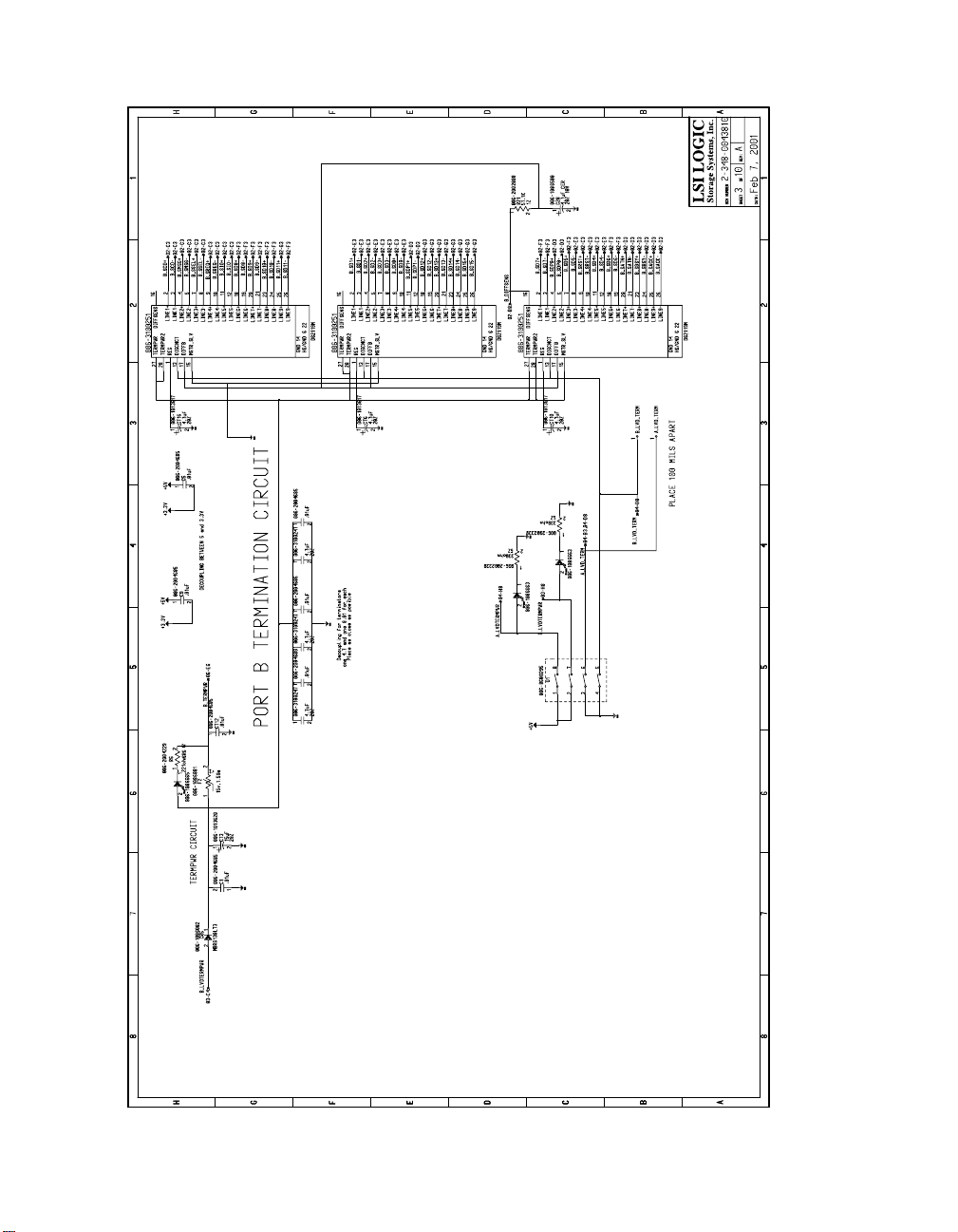
Figure A.2 LSI53C320 Wiring Diagram 2 of 4
LSI53C320 Ultra320 SCSI Bus Expander Technical Manual A-3
Version 2.2 Copyright © 2003 by LSI Logic Corporation. All rights reserved.
Page 62

Figure A.3 LSI53C320 Wiring Diagram 3 of 4
A-4 Wiring Diagrams
Version 2.2 Copyright © 2003 by LSI Logic Corporation. All rights reserved.
Page 63
Figure A.4 LSI53C320 Wiring Diagram 4 of 4
LSI53C320 Ultra320 SCSI Bus Expander Technical Manual A-5
Version 2.2 Copyright © 2003 by LSI Logic Corporation. All rights reserved.
Page 64

A-6 Wiring Diagrams
Version 2.2 Copyright © 2003 by LSI Logic Corporation. All rights reserved.
Page 65

Appendix B
Glossary
Block A block is the basic 512 byte size of storage that the storage media is
divided into. The Logical Block Address protocol uses sequential block
addresses to access the media.
Bus Expander Bus expander technology permits the extension of a bus by providing
some signal filtering and retiming to maintain signal skew budgets.
Device A single unit on the SCSI bus, identifiable by a SCSI address. It can be a
processor unit, a storage unit (such as a disk or tape controller or drive),
an output unit (such as a controller or printer), or a communications unit.
Differential A signaling alternative that employs differential drivers and receivers to
improve signal-to-noise ratios and increase maximum cable lengths.
Double
Transition
Clocking
Host A processor, usually consisting of the central processing unit and main
Initiator ASCSI device that requests another SCSI device(a target) to perform an
Logical Unit The logical representation of a physical or virtual device, addressable
LVD Low Voltage Differential. LVD is a robust design methodology that
In Double Transition (DT) Clocking data is sampled on both the asserting
and deasserting edge of the REQ/ACK signal. DT clocking may only be
implemented on an LVD SCSI bus.
memory. Typically, a host communicates with other devices, such as
peripherals and other hosts. On the SCSI bus, a host has a SCSI
address.
operation. Usually, a host acts as an initiator and a peripheral device acts
as a target.
through a target. A physical device can have more than one logical unit.
improvespower consumption, data integrity, cable lengths and support for
multiple devices, while providing a migration path for increased I/O
performance.
LSI53C320 Ultra320 SCSI Bus Expander Technical Manual B-1
Version 2.2 Copyright © 2003 by LSI Logic Corporation. All rights reserved.
Page 66

Negation The act of driving a signal to the false state or allowing the cable
terminators to bias the signal to the false state.
Parity A method of checking the accuracy of binary numbers. An extra bit, called
a parity bit, is added to a number. If even parity is used, the sum of all 1s
in the number and its corresponding parity is always even. If odd parity is
used, the sum of the 1s and the parity bit is always odd.
Port A connection into a bus.
Priority The ranking of the devices on the bus during arbitration.
Receiver The circuitry that receives electrical signals on a line.
Reconnect The function that occurs when a target reselects an initiator to continuean
operation after a disconnect.
Reselect A target can disconnect from an initiator in order to perform a time-
consuming function, such as a disk seek. After performing the operation,
the target can “reselect” the initiator.
Target A SCSI device that performs an operation requested by an initiator.
Termination The electrical connection at each end of the SCSI bus, composed of a set
of resistors.
TolerANT A technology developed and used by LSI Logic to improve data integrity,
data transfer rates, and noise immunity through the use of active
negation and input signal filtering.
Ultra320 SCSI A standard for SCSI data transfers. It allows a transfer rate of up to
320 Mbytes/s over a 16-bit SCSI bus. STA (SCSI Trade Association)
supports using the terms “Ultra320 SCSI” over the term “Fast-160.”
B-2 Glossary
Version 2.2 Copyright © 2003 by LSI Logic Corporation. All rights reserved.
Page 67

Index
Numerics
272-ball plastic ball grid array 1-8
3-state
leakage 4-4
40 MHz oscillator 3-5
A
A_DIFFSENS 2-7
A_SACK 3-3
A_SATN 3-3
A_SBSY 2-12
A_SCD 2-14
A_SD[15:0] 3-3
A_SDP[1:0] 3-3
A_SIO 3-3
A_SMSG 3-3
A_SREQ 2-13
A_SRST 2-12
A_SSEL 2-11
absolute maximum stress ratings 4-1
AC characteristics 4-7
applications 1-3
attention signal
(SATN) 2-14
, 3-3
, 3-3
, 3-3
B
B_DIFFSENS 2-7
B_SACK 3-4
B_SATN 3-4
B_SBSY 2-12
B_SCD 3-4
B_SD[15:0] 3-4
B_SDP[1:0] 3-4
B_SIO 3-4
B_SMSG 3-4
B_SRST 2-12
B_SSEL 2-11
backward compatibility 1-6
bidirectional SCSI signals 4-4
block B-1
BSY_LED 3-5
bus
timing 2-3
bus expander B-1
busy
filters 2-15
busy control
SBSY 2-12
, 3-4
, 3-4
busy LED 3-5
C
cable length 2-9
calibration 2-3
CHIP_RESET/ 3-5
CLOCK 3-5
clock
signal 2-11
skew control 2-6
clock signal 3-6
control signals
input 4-5
output 4-5
, 2-7
CRC 1-5
current 4-2
cyclic redundancy check 2-7
D
data
path 2-14
signal 2-11
data signal 3-6
DC characteristics 4-1
delay line structures 2-14
delay settings 2-3
device B-1
differential B-1
transceivers 1-6
DIFFSENS 2-7
LVD receivers 2-3
SCSI signal 4-4
distance requirements 1-3
domain validation 1-6
double transition clocking 2-4
drive strength 1-6
DT clocking 2-4
dynamic transmission mode
changing 2-8
, 4-5
, 1-4–1-5, 2-8
, B-1
, 2-5
, B-1
E
EEPROM 2-15, 3-6
electrical cable length 2-9
electrical characteristics 4-1
electrostatic discharge 4-1
enable/disable SCSI transfers 3-5
ESD 4-1
LSI53C320 Ultra320 SCSI Bus Expander Technical Manual IX-1
Version 2.2 Copyright © 2003 by LSI Logic Corporation. All rights reserved.
Page 68

F
filter edges 2-13
functional signal grouping 3-2
H
high voltage differential 1-1
host B-1
host adapter B-1
I
I/O voltage 4-2
information unit 2-6
Initiator B-1
initiator B-1
input
capacitance 4-5
I/O pads 4-5
input pads 4-5
low voltage 4-4
voltage 4-1
input clock signals 2-15
input control signals
CLOCK, RESET/, WS_ENABLE/ 4-5
intersymbol interference 1-5
, 2-4
ISI 1-5
J
junction temperature 4-2
L
latch-up current 4-1, 4-2
leading edge filter 2-11
LED 3-5
load bus 2-11
logical unit B-1
low voltage differential 1-1
LSI53C320
272-ball BGA (left half) 4-12
272-ball BGA (right half) 4-13
additional control capability 1-2
applications 1-3
clock 3-5
dynamic transmission mode 2-8
features 1-7
independent RBIAS pins 1-1
processing data 2-11
receiver logic 2-11
retiming logic 2-2
server clustering 1-3
, B-1
LVD 2-8
driver SCSI signals 4-2
receiver SCSI signals 4-3
LVDlink 1-6
features 1-6
transceivers 1-6
, 2-12
, 2-7
M
master reset 3-5
maximum cable lengths 2-8
migration path 1-6
N
negation B-2
nexus 2-3
O
on-chip RAM 2-3
operating conditions 4-2
operating free air 4-2
output
low voltage 4-4
output control signals
BSY_LED, XFER_ACTIVE 4-5
P
P1 line 2-4
paced transfers 2-4
packetized protocol 2-6
parity B-2
physical cable length 2-9
port B-2
PPR 2-5
precision delay control 2-3
precompensation 2-5
priority B-2
pulse width 2-13
, 2-10
R
receiver B-2
latch 2-11
reconnect B-2
REQ/ACK input signals 2-15
request
(REQ) 2-13
reselect B-2
reset control
signals 2-12
RESET/ signal 3-5
retiming logic 2-2
S
S_CLK 3-6
S_DATA 3-6
SACK 2-13
SCSI
A side interface pins 3-3
B side interface pins 3-4
bidirectional
signals 4-4
bus distance requirements 1-4
bus mode changing 2-8
CRC 2-7
DIFFSENS signal 4-4
DT clocking 2-4
information unit transfers 2-6
ISI 2-4
paced transfers 2-4
packetized transfers 2-6
parallel interconnect 3 1-7
, 2-8
IX-2 Index
Version 2.2 Copyright © 2003 by LSI Logic Corporation. All rights reserved.
Page 69

phases 2-3
precompensation 2-5
skew compensation 2-6
termination 2-8
TolerANT technology 1-7
Ultra320 B-2
features 2-4
SE 2-8
select (SSEL) 2-11
self-calibration 2-14
serial EEPROM 2-15
server clustering 1-3
signal
groupings 2-11
skew 2-2
signal drive strength 2-5
signals
busy control 2-12
reset control 2-12
select control 2-11
single-ended 1-1
skew compensation 1-5
slew rate 1-6
source bus 2-2
SP_CLK 2-15
SP_DAT 2-15
SREQ 2-13
state machine control 2-3
storage temperature 4-1
supply voltage 4-1
SureLINK 1-6
, 3-6
, 3-1
, 2-11
, 4-2
T
target B-2
termination B-2
test conditions
rise/fall time 4-7
thermal resistance 4-2
TolerANT 1-7
electrical characteristics 4-6
transceivers
LVDlink multimode 1-6
transfer active 3-5
transfers
information units 2-6
packetized 2-6
transmission mode
distance requirements 1-5
, B-2
V
VDD_CORE 3-6
VDD_SCSI 3-6
voltage 4-2
voltage levels
DIFFSENS 2-7
W
warm swap 3-5
WS_ENABLE/ 3-5
X
XFER_ACTIVE 3-5
, 2-6
, 4-7
U
Ultra160 SCSI
DT clocking 2-4
Ultra320 SCSI 1-5
benefits 1-5
CRC 2-7
DT clocking 2-4
features 2-4
information unit 2-6
ISI 1-5
maximum cable length 2-8
paced transfers 2-4
packetized transfers 2-6
precompensation 2-5
skew compensation 1-5
, 2-3, B-2
, 2-4
, 2-6
Index IX-3
Version 2.2 Copyright © 2003 by LSI Logic Corporation. All rights reserved.
Page 70

IX-4 Index
Version 2.2 Copyright © 2003 by LSI Logic Corporation. All rights reserved.
Page 71

Customer Feedback
We would appreciate your feedback on this document. Please copy the
following page, add your comments, and fax it to us at the number
shown.
If appropriate, please also fax copies of any marked-up pages from this
document.
Important: Please include your name, phone number, fax number, and
company address so that we may contact you directly for
clarification or additional information.
Thank you for your help in improving the quality of our documents.
LSI53C320 Ultra320 SCSI Bus Expander Technical Manual
Version 2.2 Copyright © 2003 by LSI Logic Corporation. All rights reserved.
Page 72

Reader’s Comments
Fax your comments to: LSI Logic Corporation
Technical Publications
M/S AF-198
Fax: 408.433.4333
Please tell us how you rate this document: LSI53C320 Ultra320 SCSI
Bus Expander Technical Manual. Place a check mark in the appropriate
blank for each category.
Excellent Good Average Fair Poor
Completeness of information ____ ____ ____ ____ ____
Clarity of information ____ ____ ____ ____ ____
Ease of finding information ____ ____ ____ ____ ____
Technical content ____ ____ ____ ____ ____
Usefulness of examples and
illustrations
Overall manual ____ ____ ____ ____ ____
____ ____ ____ ____ ____
What could we do to improve this document?
If you found errors in this document, please specify the error and page
number. If appropriate, please fax a marked-up copy of the page(s).
Please complete the information below so that we may contact you
directly for clarification or additional information.
Name Date
Telephone
Fax
Title
Department Mail Stop
Company Name
Street
City, State, Zip
Customer Feedback
Version 2.2 Copyright © 2003 by LSI Logic Corporation. All rights reserved.
Page 73

You can find a current list of our U.S. distributors, international distributors, and sales
offices and design resource centers on our web site at
http://www.lsilogic.com/contacts/index.html
Page 74

 Loading...