

Page 1

TECHNICAL
MANUAL
LSI53C180
Ultra160 SCSI
Bus Expander
Version 1.3
June 2001
®
S14041.C
Page 2

This document contains proprietary information of LSI Logic Corporation. The
information contained herein is not to be used by or disclosed to third parties
without the express written permission of an officer of LSI Logic Corporation.
LSI Logic products are not intended for use in life-support appliances, devices,
or systems. Use of any LSI Logic product in such applications without written
consent of the appropriate LSI Logic officer is prohibited.
Document DB14-000118-03, Fourth Edition (June 2001)
This document describes the LSI Logic Corporation LSI53C180 Ultra160 SCSI
Bus Expander and will remain the official reference source for all
revisions/releases of this product until rescinded by an update.
To receive product literature, visit us at http://www.lsilogic.com.
LSI Logic Corporation reserves the right to make changes to any products herein
at any time without notice. LSI Logic does not assume any responsibility or
liability arising out of the application or use of any product described herein,
except as expressly agreed to in writing by LSI Logic; nor does the purchase or
use of a product from LSI Logic convey a license under any patent rights,
copyrights, trademark rights, or any other of the intellectual property rights of
LSI Logic or third parties.
Copyright © 2000-2001 by LSI Logic Corporation. All rights reserved.
TRADEMARK ACKNOWLEDGMENT
The LSI Logic logo design, LVD Link, and TolerANT are trademarks or registered
trademarks of LSI Logic Corporation. All other brand and product names may be
trademarks of their respective companies.
MH
ii
Page 3

Audience
Preface
This manual provides a description of the LSI53C180 Ultra160 SCSI Bus
Expander chip that supports all combinations of Single-Ended and Low
Voltage Differential SCSI bus conversions.
Currently the LSI53C140 is offered in a 192-BGA package so that
customers who are designing Ultra2 can easily upgrade to Ultra160.
Refer to System Engineering Note S11006 for design considerations
using the LSI53C140 and LSI53C180.
This manual assumes some prior knowledge of current and proposed
SCSI standards. For background information, please contact:
ANSI
11 West 42nd Street
New York, NY 10036
(212) 642-4900
Ask for document number X3.131-199X (SCSI-2)
Global Engineering Documents
15 Inverness Way East
Englewood, CO 80112
(800) 854-7179 or (303) 397-7956 (outside U.S.)
FAX (303) 397-2740
Ask for document number X3.131-1994 (SCSI-2) or
X3.253 (SCSI Parallel Interface-3 (SPI-3))
Preface iii
Page 4

Organization
ENDL Publications
14426 Black Walnut Court
Saratoga, CA 95070
(408) 867-6642
Document names: SCSI Bench Reference, SCSI Encyclopedia,
SCSI Tutor
Prentice Hall
113 Sylvan Avenue
Englewood Cliffs, NJ 07632
(800) 947-7700
Ask for document number ISBN 0-13-796855-8,
SCSI: Understanding the Small Computer System Interface
LSI Logic World Wide Web Home Page
www.lsil.com
This document has the following chapters and appendixes:
• Chapter 1, Introduction, contains the general information about the
LSI53C180 product.
• Chapter 2, Functional Descriptions, describes the main functional
areas of the chip in more detail, including the interfaces to the SCSI
bus and external memory.
• Chapter 3, Specifications, contains the pin diagram, signal
descriptions, electrical characteristics, AC timing diagrams, and
mechanical drawing of the LSI53C180.
• Appendix A, Wiring Diagrams, contains wiring diagrams that show
typical LSI53C180 usage.
• Appendix B, Glossary, contains commonly used terms and their
definitions.
iv Preface
Page 5
Revision Record
Date Version Remarks
2/00 1.0 Version 1.0
11/00 1.1 All product names changed from SYM to LSI.
4/01 1.2 Changes in Chapter 2 to how Warm Swap Enable is
6/01 1.3 Changes to wiring diagrams in Appendix A.
designated. Changes in Chapter 3 to DC
Characteristics.
Preface v
Page 6

vi Preface
Page 7

Contents
Chapter 1 Introduction
1.1 General Description 1-1
1.1.1 Applications 1-3
1.1.2 Features 1-5
1.1.3 Specifications 1-6
1.2 Ultra160 SCSI 1-6
1.2.1 Double Transition (DT) Clocking 1-6
1.2.2 Cyclic Redundancy Check (CRC) 1-6
1.2.3 Domain Validation 1-7
1.2.4 Parallel Protocol Request 1-7
1.2.5 Benefits of LVD Link 1-7
Chapter 2 Functional Descriptions
2.1 Interface Signal Descriptions 2-1
2.1.1 SCSI A Side and B Side Control Blocks 2-2
2.1.2 Retiming Logic 2-4
2.1.3 Precision Delay Control 2-4
2.1.4 State Machine Control 2-4
2.1.5 DIFFSENS Receiver 2-5
2.1.6 Dynamic Transmission Mode Changes 2-5
2.1.7 SCSI Signal Descriptions 2-5
2.1.8 Control Signals 2-11
2.1.9 SCSI Termination 2-13
2.2 Internal Control Descriptions 2-14
2.2.1 Self-Calibration 2-14
2.2.2 Delay Line Structures 2-14
2.2.3 Busy Filters 2-15
Contents vii
Page 8

Chapter 3 Specifications
3.1 Signal Descriptions 3-1
3.2 Electrical Characteristics 3-7
3.2.1 DC Characteristics 3-8
3.2.2 TolerANT Technology Electrical Characteristics 3-12
3.2.3 AC Characteristics 3-16
3.2.4 SCSI Interface Timing 3-16
3.3 Mechanical Drawings 3-19
3.3.1 LSI53C180 192-Pin BGA Mechanical Drawing 3-20
Appendix A Wiring Diagrams
A.1 LSI53C180 Wiring Diagrams A-1
Appendix B Glossary
Index
Customer Feedback
Figures
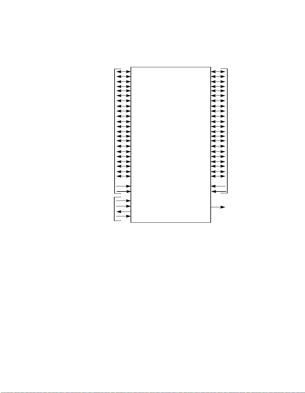
1.1 LSI53C180 SCSI Bus Modes 1-2
1.2 LSI53C180 Server Clustering 1-3
1.3 LSI53C180 SCSI Bus Device 1-4
2.1 LSI53C180 Block Diagram 2-2
2.2 LSI53C180 Signal Grouping 2-6
3.1 Left Half of LSI53C180 192-Pin BGA Top View 3-2
3.2 Right Half of LSI53C180 192-Pin BGA Top View 3-3
3.3 LSI53C180 Functional Signal Grouping 3-4
3.4 LVD Driver 3-9
3.5 LVD Receiver 3-10
3.6 External Reset Circuit 3-12
3.7 Rise and Fall Time Test Conditions 3-14
3.8 SCSI Input Filtering 3-14
3.9 Hysteresis of SCSI Receivers 3-14
3.10 Input Current as a Function of Input Voltage 3-15
viii Contents
Page 9

Tables
3.11 Output Current as a Function of Output Voltage 3-15
3.12 Clock Timing 3-16
3.13 Input/Output Timing - Single Transition 3-17
3.14 Input/Output Timing - Double Transition 3-18
3.15 192-Pin PBGA (IJ, I2) Mechanical Drawing 3-20
A.1 LSI53C180 Wiring Diagram 1 of 4 A-2
A.2 LSI53C180 Wiring Diagram 2 of 4 A-3
A.3 LSI53C180 Wiring Diagram 3 of 4 A-4
A.4 LSI53C180 Wiring Diagram 4 of 4 A-5
1.1 Types of Operation 1-2
1.2 SCSI Bus Distance Requirements 1-4
1.3 Transmission Mode Distance Requirements 1-4
2.1 DIFFSENS Voltage Levels 2-5
2.2 Mode Sense Control Voltage Levels 2-11
2.3 RESET/ Control Signal Polarity 2-12
2.4 WS_ENABLE Signal Polarity 2-12
2.5 XFER_ACTIVE Signal Polarity 2-13
3.1 SCSI A Side Interface Pins 3-5
3.2 SCSI B Side Interface Pins 3-6
3.3 Chip Interface Control Pins 3-6
3.4 Power and Ground Pins 3-7
3.5 Absolute Maximum Stress Ratings 3-8
3.6 Operating Conditions 3-8
3.7 LVD Driver SCSI Signals—B_SD[15:0]±, B_SDP[1:0]±,
B_SCD±, B_SIO±, B_SMSG±, B_SREQ±, B_SACK±,
B_SBSY±, B_SATN±, B_SSEL±, B_SRST± 3-9
3.8 LVD Receiver SCSI Signals—B_SD[15:0]±, B_SDP[1:0]±,
B_SCD±, B_SIO±, B_SMSG±, B_SREQ±, B_SACK±,
B_SBSY±, B_SATN±, B_SSEL±, B_SRST± 3-9
3.9 DIFFSENS SCSI Signal 3-10
3.10 Input Capacitance 3-10
3.11 Bidirectional SCSI Signals—A_SD[15:0]/, A_SDP[1:0]/,
A_SREQ/, A_SACK/, B_SD[15:0]±, B_SDP[1:0]±,
B_SREQ±, B_SACK± 3-11
Contents ix
Page 10

3.12 Bidirectional SCSI Signals—A_SCD/, A_SIO/,
A_SMSG/, A_SBSY/, A_SATN/, A_SSEL/, A_SRST/,
B_SCD±, B_SIO±, B_SMSG±, B_SBSY±, B_SATN±,
B_SSEL±, B_SRST± 3-11
3.13 Input Control Signals—CLOCK, RESET/, WS_ENABLE 3-11
3.14 Output Control Signals—BSY_LED, XFER_ACTIVE 3-12
3.15 TolerANT Technology Electrical Characteristics 3-12
3.16 Clock Timing 3-16
3.17 Input Timing - Single Transition 3-16
3.18 Output Timing - Single Transition 3-17
3.19 Input Timing - Double Transition 3-17
3.20 Output Timing - Double Transition 3-18
x Contents
Page 11

Chapter 1
Introduction
This chapter describes the LSI53C180 Ultra160 SCSI Bus Expander and
its applications. It includes these sections:
• Section 1.1, “General Description,” page 1-1
• Section 1.2, “Ultra160 SCSI,” page 1-6
1.1 General Description
The LSI53C180 Ultra160 SCSI Bus Expander is a single chip solution
allowing the extension of SCSI device connectivity and/or cable length
limits. A SCSI bus expander couples bus segments together without any
impact to the SCSI protocol, software, or firmware. The LSI53C180
Ultra160 SCSI Bus Expander connects Single-Ended (SE) Ultra and Low
Voltage Differential (LVD) Ultra160 peripherals together in any
combination. The LSI53C180 does not support High Voltage Differential
(HVD) mode.
The LSI53C180 is capable of supporting any combination of SE or LVD
bus mode on either the A or B Side port. This provides the system
designer with maximum flexibility in designing SCSI backplanes to
accommodate any SCSI bus mode. The LSI53C180 has independent
RBIAS pins allowing margining for each bus. A 10 kΩ pull-up resistor on
RBIAS is required to provide the correct LVD levels.
LSI53C180 Ultra3 SCSI Bus Expander 1-1
Page 12

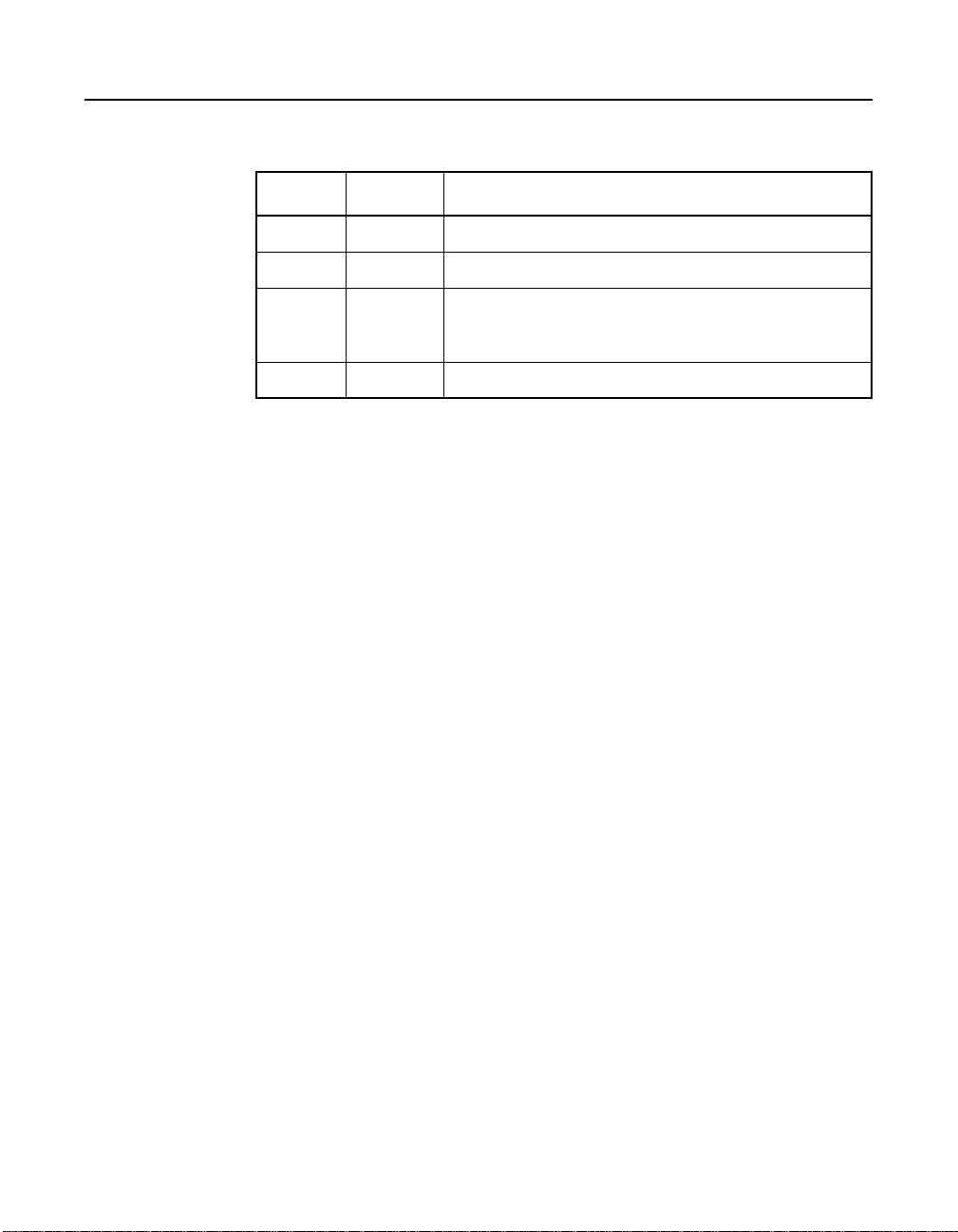
Figure 1.1 LSI53C180 SCSI Bus Modes
A Side B Side
LVD
SE
LSI53C180
SCSI Expander
192 PBGA
LVD
SE
Figure 1.1 shows the two SCSI bus modes available on the A or B Side.
LVD Link™ transceivers provide the multimode LVD or SE capability. The
LSI53C180 operates as both an expander and converter. In both SCSI
Bus Expander and Converter modes, cable segments are isolated from
each other. This feature maintains the signal integrity of each cable
segment.
Table 1.1 shows the types of operational modes for the LSI53C180.
Table 1.1 Types of Operation
Signal Type Speed
LVD to LVD Ultra160
SE to SE Ultra
LVD to SE Ultra
SE to LVD Ultra
The LSI53C180 provides additional control capability through the pin
level isolation mode (Warm Swap Enable). This feature permits logical
disconnection of both the A Side bus and the B Side bus without
disrupting SCSI transfers currently in progress. For example, devices on
the logically disconnected B Side can be swapped out while the A Side
bus remains active.
The LSI53C180 is based on previous bus expander technology, which
includes signal filtering along with retiming to maintain skew budgets.
The LSI53C180 is independent of software.
1-2 Introduction
Page 13
1.1.1 Applications
• Server clustering environments
• Expanders creating distinct SCSI cable segments that are isolated
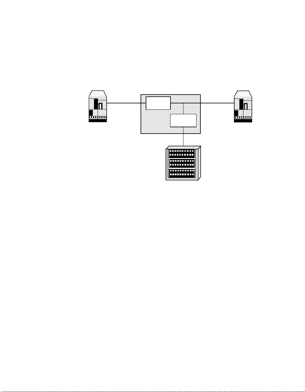
Figure 1.2 LSI53C180 Server Clustering
from each other
Primary Server
Segment A
SCSI Bus
Expander
SCSI Bus
Expander
Segment C
Shared Disk Subsystem
Segment B
Secondary Server
Figure 1.2 demonstrates how SCSI bus expanders are used to couple
bus segments together without any impact on the SCSI protocol or
software. Configurations that use the LSI53C180 SCSI Bus Expander in
the Ultra160 mode (LVD to LVD) allow the system designer to take
advantage of the inherent cable distance, device connectivity, data
reliability, and increased transfer rate benefits of LVD signaling with
Ultra160 SCSI peripherals.
In the Figure 1.2 example, two LSI53C180 expanders are used to
configure three segments. This configuration allows segment A to be
treated as a point-to-point segment. Segments B and C are treated as
load segments with at least 8 inches between every node. Table 1.2
shows the various distance requirements for each SCSI bus mode.
General Description 1-3
Page 14
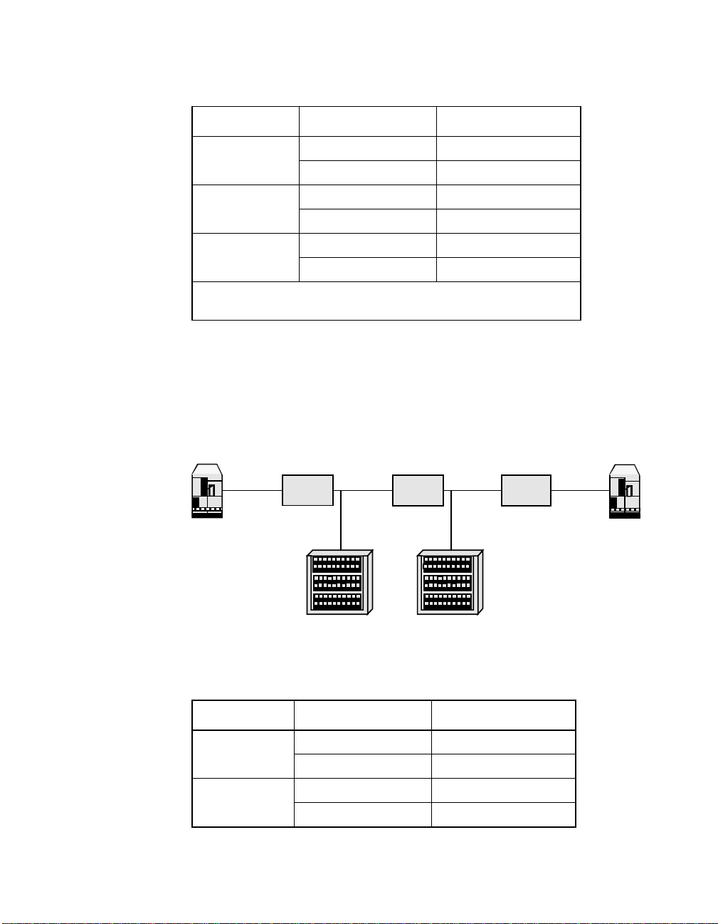
Table 1.2 SCSI Bus Distance Requirements
Segment Mode Length Limit
A LVD (Ultra160) 25 meters
SE (Ultra) 3 meters
1
B LVD (Ultra160) 12 meters
SE (Ultra) 1.5 meters
C LVD (Ultra160) 12 meters
SE (Ultra) 1.5 meters
1. The length may be more, possibly 6 meters, as no devices are
attached to it.
In the second example, Figure 1.3, the LSI53C180 is cascaded to
achieve four distinct SCSI segments. Segments A and D can be treated
as point-to-point segments. Segments B and C are treated as load
segments with at least 8-inch spacing between every node.
Figure 1.3 LSI53C180 SCSI Bus Device
Segment A Segment B Segment C
Primary
Server
Table 1.3 Transmission Mode Distance Requirements
Segment Mode Length Limit
A, D LVD (Ultra160) 25 meters
B, C LVD (Ultra160) 12 meters
1-4 Introduction
SCSI Bus
Expander
Shared Disk
Subsystem
SCSI Bus
Expander
Shared Disk
Subsystem
SCSI Bus
Expander
SE (Ultra) 1.5 meters
SE (Ultra) 1.5 meters
Segment D
Secondary
Server
Page 15

1.1.2 Features
• A flexible SCSI bus expander that supports any combination of LVD
or SE transceivers
• Creates distinct SCSI bus segments that are isolated from each
other
• Integrated LVD Link transceivers for direct attachment to either LVD
or SE bus segments
• Operates as a SCSI Bus Expander
– LVD to LVD (Ultra160 SCSI)
– SE to SE (Ultra SCSI)
• Operates as a SCSI Bus Converter
– LVD to SE (Ultra SCSI)
– SE to LVD (Ultra SCSI)
• Targets and initiators may be located on either the A or B Side of the
device
• Accepts any asynchronous or synchronous transfer speed up to
Ultra160 SCSI (for LVD to LVD mode only)
• Supports dynamic addition/removal of SCSI bus segments using the
isolation mode
• Does not consume a SCSI ID
• Propagates the RESET/ signal from one side to the other regardless
of the SCSI bus state
• Notifies initiator(s) of changes in transmission mode (SE/LVD) on A
or B Side segments by using the SCSI bus RESET/
• SCSI Busy LED driver for activity indicator
• Up to four LSI53C180s may be cascaded
• Does not require software
• Supports Double Transition (DT) clocking
• Supports Cyclic Redundancy Check (CRC) in DT data phases
• Supports Domain Validation
General Description 1-5
Page 16

1.1.3 Specifications
• 40 MHz Input Clock
• 192-pin Plastic Ball Grid Array package (PBGA). This package is a
drop in replacement for the LSI53C140 when the design uses the
LSI53C180 pinout.
• Compliant with the SCSI Parallel Interface-3 (SPI-3)
• Compliant with SCSI Enhanced Parallel Interface (EPI) Specifications
1.2 Ultra160 SCSI
The LSI53C180 SCSI Bus Expander supports Ultra160 SCSI. This
interface is an extension of the SCSI-3 standards that expands the
bandwidth of the SCSI bus to allow faster synchronous data transfers,
up to 160 Mbytes/s. Ultra160 SCSI provides a doubling of the data rate
over the Ultra2 SCSI interface. All new speeds after Ultra2 are wide.
1.2.1 Double Transition (DT) Clocking
Ultra160 provides DT clocking for LVD transfers where clocking is
defined on the rising and falling edges of the clock. The latching of data
on both the assertion edge and the negation edge of the REQ/ACK
signal represents DT data phases. DT data phase encompasses both the
DT Data In and the DT Data Out phase. DT data phases use only 16bit, synchronous transfers.
Information unit and data group transfers use DT data phases to transfer
data. Information unit transferstransmitallnexus, task management, task
attribute, command, data, and protection. Data group transfers transmit
all data and protection. The number of bytes transferred for an
information unit or data group is always a multiple of four. Refer to the
SCSI Parallel Interface-3 (SPI-3) for more detailed information about
DT clocking.
1.2.2 Cyclic Redundancy Check (CRC)
Ultra160 supports CRC, which represents error checking code to detect
the validity of data. CRC increases the reliability of data transfers since
four bytes of code are transferred along with data. All single bit errors,
1-6 Introduction
Page 17

two bits in error, or other error types within a single 32-bit range are
detected. Refer to SPI-3 to see how CRC generation and transmission
occur during data transfers.
1.2.3 Domain Validation
Domain Validation is a procedure that allows a host computer and target
SCSI peripheral to negotiate and find the optimal transfer speed. This
procedure improves overall reliability of the system by ensuring integrity
of the data transferred.
1.2.4 Parallel Protocol Request
Parallel Protocol Request (PPR) messages negotiate a synchronous
data transfer agreement, a wide data transfer agreement, and set the
protocol options between two SCSI devices. This message exchange
negotiates limits about data transmission and establishes an agreement
between the two SCSI devices. This agreement applies to ST Data In,
ST Data Out, DT Data In, and DT Data Out phases.
For example, a SCSI device could initiate a PPR message whenever it
is appropriate to negotiate a data transfer agreement. If the target device
is capable of supporting any of the PPR options, it will respond with a
PPR message. If not, it responds with a Message Reject message and
the two SCSI devices use either SDTR or WDTR messages to negotiate
an agreement.
1.2.5 Benefits of LVD Link
The LSI53C180 supports LVD technology for SCSI, a signaling
technology that increases the reliability of SCSI data transfers over
longer distances than those supported by SE SCSI technology. The low
current output of LVD allows the I/O transceivers to be integrated directly
onto the chip. LVD provides the reliability of HVD SCSI technology
without the added cost of external differential transceivers. LVD allows a
longer SCSI cable and more devices on the bus. LVD provides a
long-term migration path to even faster SCSI transfer rates without
compromising signal integrity, cable length, or connectivity.
For backward compatibility to existing SE devices, the LSI53C180
features multimode LVD Link transceivers that can switch between LVD
and SE modes.
Ultra160 SCSI 1-7
Page 18

Some features of integrated LVD Link multimode transceivers are:
• Supports SE or LVD technology
• Allows greater device connectivity and longer cable length
• LVD Link transceivers save the cost of external differential
transceivers
• Supports a long-term performance migration path
1-8 Introduction
Page 19

Chapter 2
Functional
Descriptions
This chapter describes all signals, their groupings, and their functions. It
includes these topics:
• Section 2.1, “Interface Signal Descriptions,” page 2-1
• Section 2.2, “Internal Control Descriptions,” page 2-14
2.1 Interface Signal Descriptions
The LSI53C180 has no programmable registers, and therefore, no
software requirements. SCSI control signals control all LSI53C180
functions. Figure 2.1 shows a block diagram of the LSI53C180 device,
which is divided into these specific areas:
• A Side SCSI Control Block
– LVD and SE Drivers and Receivers
• B Side SCSI Control Block
– LVD and SE Drivers and Receivers
• Retiming Logic
• Precision Delay Control
• State Machine Control
LSI53C180 Ultra3 SCSI Bus Expander 2-1
Page 20
Figure 2.1 LSI53C180 Block Diagram
Control
Signals
LVD, Single-ended,
Wide Ultra SCSI Bus
(A Side)
ansceivers
VD Link Tr
L
ol Block
SCSI Contr
Retiming
Logic
k
ol Bloc
LVD Link Transceivers
SCSI Contr
LVD, Single-ended
Wide Ultra SCSI Bus
(B Side)
Precision
er
A_DIFFSENS B_DIFFSENS
VD
L
Control
Receiv
DIFFSENS
Delay
40 MHz Clock Input
In its simplest form, the LSI53C180 passes data and parity from a source
bus to a load bus. The side asserting, deasserting, or releasing the SCSI
signals is the source side. The model of the LSI53C180 represents
pieces of wire that allow corresponding SCSI signals to flow from one
side to the other side. The LSI53C180 monitors arbitration and selection
by devices on the bus so it can enable the proper drivers to pass the
signals along. In addition, the LSI53C180 does signal retiming to
maintain the signal skew budget from the source bus to the load bus.
2.1.1 SCSI A Side and B Side Control Blocks
The SCSI A Side pins are connected internally to the corresponding
SCSI B Side pins, forming bidirectional connections to the SCSI bus.
In the LVD/LVD mode, the SCSI A Side and B Side control blocks
connect to both targets and initiators and accept any asynchronous or
synchronous data transfer rates up to the 160 Mbytes/s rate of Wide
Ultra160 SCSI. TolerANT®and LVD Link technologies are part of both
the A Side and B Side control blocks.
State
Machine
Control
LVD
Receiver
DIFFSENS
2.1.1.1 LSI53C180 Requirements for Synchronous Negotiation
The LSI53C180 builds a table of information regarding devices on the
bus in on-chip RAM. The PPR, SDTR, and WDTR information for each
2-2 Functional Descriptions
Page 21

device is taken from the MSG bytes during negotiation. For all devices
in the configuration to communicate accurately through the LSI53C180
at Ultra160 (Fast-80) rates, it is necessary for a complete synchronous
negotiation to take place between the initiator and target(s) prior to any
data transfer. On a 16-bit bus, the LSI53C180 at Ultra160 approaches
rates of 160 Mbytes/s. The LSI53C180 defaults to Fast-20 rates when a
valid negotiation between the initiator and target has not occurred.
2.1.1.2 TolerANT Technology
In SE mode, the LSI53C180 features TolerANT technology, which
includes active negation on the SCSI drivers and input signal filtering on
the SCSI receivers. Active negation causes the SCSI Request,
Acknowledge, Data, and Parity signals to be actively driven HIGH rather
than passively pulled up by terminators.
TolerANT receiver technology improves data integrity in unreliable
cabling environments, where other devices would be subject to data
corruption. TolerANT receivers filter the SCSI bus signals to eliminate
unwanted transitions without the long signal delays associated with
RC-type input filters. This improved driver and receiver technology helps
eliminate double clocking of data, the single biggest reliability issue with
SCSI operations.
The benefits of TolerANT technology include increased immunity to noise
on the deasserting signal edge, better performance due to balanced duty
cycles, and improved SCSI transfer rates. In addition, TolerANT SCSI
devices prevent glitches on the SCSI bus at power-up or power-down, so
other devices on the bus are also protected from data corruption.
2.1.1.3 LVD Link Technology
To support greater device connectivity and longer SCSI cables, the
LSI53C180 features LVD Link technology, the LSI Logic implementation
of multimode LVD SCSI. LVD Link transceivers provide the inherent
reliability of differential SCSI, and a long-term migration path of faster
SCSI transfer rates.
LVD Link technology is based on current drive. Its low output current
reduces the power needed to drive the SCSI bus. Therefore, the I/O
drivers can be integrated directly onto the chip. This reduces the cost and
complexity compared to traditional (high power) differential designs.
Interface Signal Descriptions 2-3
Page 22

LVD Link lowers the amplitude of noise reflections and allows higher
transmission frequencies.
The LVD Link transceivers in Side A and Side B operate in the LVD or
SE modes. The LSI53C180 automatically detects the type of signal
connected, based on the voltages detected by A_DIFFSENS and
B_DIFFSENS.
2.1.2 Retiming Logic
The SCSI signals, as they propagate from one side of the LSI53C180 to
the other side, are processed by logic circuits that retime the bus signals,
as needed, to guarantee or improve the required SCSI timings. The
retiming logic is governed by the State Machine Controls that keep track
of SCSI phases, the location of initiator and target devices, and various
timing functions. In addition, the retiming logic contains numerous delay
elements that are periodically calibrated by the Precision Delay Control
block in order to guarantee specified timing such as output pulse widths,
setup and hold times, and other elements.
When a synchronous negotiation takes place between devices, a nexus
is formed, and the corresponding information on that nexus is stored in
the on-chip RAM. This information remains in place until a chip reset,
power down, or renegotiation occurs. This enables the chip to make
more accurate retiming adjustments.
2.1.3 Precision Delay Control
The Precision Delay Control block provides calibration information to the
precision delay elements in the Retiming Logic block. This calibration
information provides precise timing as signals propagate through the
device. As the LSI53C180 voltage and temperature vary over time, the
Precision Delay Control block periodically updates the delay settings in
the Retiming Logic. The purpose of these updates is to maintain constant
and precise control over bus timing.
2.1.4 State Machine Control
The State Machine Control tracks the SCSI bus phase protocol and other
internal operating conditions. This block provides signals to the Retiming
Logic that identify how to properly handle SCSI bus signal retiming based
on SCSI protocol.
2-4 Functional Descriptions
Page 23

2.1.5 DIFFSENS Receiver
The LSI53C180 contains LVD DIFFSENS receivers that detect the
voltage level on the A Side or B Side DIFFSENS lines to inform the
LSI53C180 of the transmission mode being used by the SCSI buses. A
device does not change its present signal driver or receiver mode based
on the DIFFSENS voltage levels unless a new mode is sensed
continuously for at least 100 ms.
Transmission mode detection for SE or LVD is accomplished through the
use of the DIFFSENS lines. Table 2.1 shows the voltages on the
DIFFSENS lines and modes they will cause.
Table 2.1 DIFFSENS Voltage Levels
Voltage Mode
−0.35 to +0.5 SE
+0.7 to +1.9 LVD
2.1.6 Dynamic Transmission Mode Changes
Any dynamic mode change (SE/LVD) on a bus segment is considered to
be a significant event that requires the initiator to determine whether the
mode change meets the requirements for that bus segment.
The LSI53C180 supports dynamic transmission mode changes by
notifying the initiator(s) of changes in transmission mode (SE/LVD) on A
or B Side segments by using the SCSI bus RESET. The DIFFSENS line
detects a valid mode switch on the bus segments. After the DIFFSENS
state is present for 100 ms, the LSI53C180 generates a SCSI reset on
the opposite bus from the one that the transmission mode change
occurred on. This reset informs any initiators residing on the opposite
segment about the change in the transmission mode. The initiator(s) then
renegotiates synchronous transfer rates with each device on that segment.
2.1.7 SCSI Signal Descriptions
For a description of a specific signal, see Section 3.1, “Signal
Descriptions,” in Chapter 3. For signal electrical characteristics, see
Section 3.2, “Electrical Characteristics.” For SCSI bus signal timing, see
Interface Signal Descriptions 2-5
Page 24
Section 3.2.4, “SCSI Interface Timing.” Figure 2.2 shows the LSI53C180
signal grouping. A description of the signal groups follows.
Figure 2.2 LSI53C180 Signal Grouping
A Side
LVD or SE
SCSI Interface
Control Signals
2.1.7.1 Data and Parity (SD and SDP)
A_SSEL+
A_SSELA_SBSY+
A_SBSYA_SRST+
A_SRSTA_SREQ+
A_SREQA_SACK+
A_SACKA_SMSG+
A_SMSGA_SCD+
A_SCDA_SIO+
A_SIOA_SATN+
A_SATNA_SDP[1:0]+
A_SDP[1:0]A_SD[15:0]+
A_SD[15:0]-
A_DIFFSENS
A_RBIAS B_RBIAS
RESET/
WS_ENABLE
XFER_ACTIVE
CLOCK
LSI53C180
B_SSEL+
B_SSEL-
B_SBSY+
B_SBSY-
B_SRST+
B_SRST-
B_SREQ+
B_SREQB_SACK+
B_SACK-
B_SMSG+
B_SMSG-
B_SCD+
B_SCD-
B_SIO+
B_SIO-
B_SATN+
B_SATN-
B_SDP[1:0]+
B_SDP[1:0]-
B_SD[15:0]+
B_SD[15:0]-
B_DIFFSENS
BSY_LED
B Side
LVD or SE
SCSI Interface
The signals named A_SD[15:0] and A_SDP[1:0] are the data and parity
signals from the A Side, and B_SD[15:0] and B_SDP[1:0] are the data
and parity signals from the B Side of the LSI53C180. These signals are
sent and received from the LSI53C180 by using SCSI compatible drivers
and receiver logic designed into the LSI53C180 interfaces. This logic
provides the multimode LVD and SE interfaces in the chip. This logic also
provides the necessary drive, sense thresholds, and input hysteresis to
function correctly in a SCSI bus environment.
The LSI53C180 receives data and parity signals and passes them from
the source bus to the load bus and provides any necessary edge shifting
to guarantee the skew budget for the load bus. Either side of the
LSI53C180 may be the source bus or the load bus. The side that is
2-6 Functional Descriptions
Page 25

asserting, deasserting, or releasing the SCSI signals is the source side.
These steps describe the LSI53C180 data processing:
1. Asserted data is accepted by the receiver logic as soon as it is
received. Once the clock signal (REQ/ACK) has been received, data
is gated from the receiver latch.
2. The path is next tested to ensure the signal if being driven by the
LSI53C180 is not misinterpreted as an incoming signal.
3. The data is then leading edge filtered. The assertion edge is held for
a specified time to prevent any signal bounce. The duration is
controlled by the input signal.
4. The next stage uses a latch to sample the signal. This provides a
stable data window for the load bus.
5. The final step develops pull-up and pull-down controls for the SCSI
I/O logic, including 3-state controls for the pull-up.
6. A parallel function ensures that bus (transmission line) recovery
occurs for a specified time after the last signal deassertion on each
signal line.
2.1.7.2 SCSI Bus Activity LED (BSY_LED)
Internal logic detects SCSI bus activity and generates a signal that
produces an active HIGH output. This output can be used to drive a LED
to indicate SCSI activity.
The internal circuitry is a digital one shot that is an active HIGH with a
minimum pulse width of 16 ms. The BSY_LED output current is 8 mA.
This output may have an LED attached to it with the other lead of the
LED grounded through a suitable resistor.
2.1.7.3 Select Control (SSEL)
A_SSEL and B_SSEL are control signals used during bus arbitration and
selection. Whichever side asserts, SSEL propagates it to the other side.
If both signals are asserted at the same time, the A Side receives SSEL
and sends it to the B Side. This output has pull-down control for an open
collector driver. The processing steps for the signals are:
Interface Signal Descriptions 2-7
Page 26

1. The input signal is blocked if it is being driven by the LSI53C180.
2. The next stage is a leading edge filter. This ensures that the output
does not switch for a specified time after the leading edge. The
duration of the input signal then determines the duration of the
output.
3. A parallel function ensures that bus (transmission line) recovery
occurs for a specified time after the last signal deassertion on each
signal line.
2.1.7.4 Busy Control (SBSY)
A_SBSY and B_SBSY signals are propagated from the source bus to the
load bus. The busy control signals go through this process:
1. The bus is tested to ensure the signal if being driven by the
LSI53C180 is not misinterpreted as an incoming signal.
2. The data is then leading edge filtered. The assertion edge is held for
a specified time to prevent any signal bounce. The input signal
controls the duration.
3. The signal path switches the long and short filters used in the circuit
depending upon the current state of the LSI53C180. The current
state of the LSI53C180 State Machine that tracks SCSI phases
selects the mode. The short filter mode passes data through, while
the long filter mode indicates the bus free state. When the Busy
(SBSY) and Select (SSEL) sources switch from side to side, the long
filter mode is used. This output is then fed to the output driver, which
is a pull-down open collector only.
4. A parallel function ensures that bus (transmission line) recovery is
availablefor a specified time after the last signal deassertion on each
signal line.
2.1.7.5 Reset Control (SRST)
A_SRST and B_SRST are also passed from the source to the load bus.
This output has pull-down control for an open collector driver. The reset
signals are processed in this sequence:
1. The input signal is blocked if it is already being driven by the
LSI53C180.
2-8 Functional Descriptions
Page 27

2. The next stage is a leading edge filter. This ensures that the output
will not switch during a specified time after the leading edge. The
duration of the input signal then determines the duration of the
output.
3. A parallel function ensures that bus (transmission line) recovery
occurs for a specified time after the last signal deassertion on each
signal line.
When the LSI53C180 senses a true mode change on either bus, it
generates a SCSI reset to the opposite bus. For example, when LVD
mode changes to SE mode, a reset occurs.
2.1.7.6 Request and Acknowledge Control (SREQ and SACK)
A_SREQ, A_SACK, B_SREQ, and B_SACK are clock and control
signals. Their signal paths contain controls to guarantee minimum pulse
widths, filter edges, and do some retiming when used as data transfer
clocks. In DT clocking, both leading and trailing edges are filtered, while
only the leading edge is filtered in single transition clocking. SREQ and
SACK have paths from the A Side to the B Side and from the B Side to
the A Side. The received signal goes through these processing steps
before being sent to the opposite bus:
1. The asserted input signal is sensed and forwarded to the next stage
if the direction control permits it. The direction controls are developed
from state machines that are driven by the sequence of bus control
signals.
2. The signal must then pass the test of not being regenerated by the
LSI53C180.
3. The next stage is a leading edge filter. This ensures that the output
does not switch during the specified hold time after the leading edge.
The duration of the input signal determines the duration of the output
after the hold time. The circuit guarantees a minimum pulse rate.
4. The next stage passes the signal if it is not a data clock. If SREQ or
SACK is a data clock, it delays the leading edge to improve data
output setup times. The input signal again controls the duration.
5. This stage is a trailing edge signal filter. When the signal deasserts,
the filter does not permit any signal bounce. The output signal
deasserts at the first deasserted edge of the input signal.
Interface Signal Descriptions 2-9
Page 28

6. The last stage develops pull-up and pull-down signals with drive and
3-state control.
7. A parallel function ensures that bus (transmission line) recovery
occurs for a specified time after the last signal deassertion on each
signal line.
2.1.7.7 Control/Data, Input/Output, Message, and Attention Controls
(SCD, SIO, SMSG, and SATN)
A_SCD, A_SIO, A_SMSG, A_SATN, B_SCD, B_SIO, B_SMSG, and
B_SATN are control signals that have the following processing steps:
1. The input signal is blocked if it is being driven by the LSI53C180.
2. The next stage is a leading edge filter. This ensures the output does
not switch for a specified time after the leading edge. The duration
of the input signal determines the duration of the output.
3. The final stage develops pull-up and pull-down controls for the SCSI
I/O logic, including 3-state controls for the pull-up.
4. A parallel function ensures that bus (transmission line) recovery is for
a specified time after the last signal deassertion on each signal line.
2.1.7.8 Multimode Signal Control
A_SD[15:0], A_SDP[1:0], A_SBSY, A_SSEL, A_SCD, A_SIO, A_SMSG,
A_SREQ, A_SACK, A_SATN, A_SRST, B_SD[15:0], B_SDP[1:0],
B_SBSY, B_SSEL, B_SCD, B_SIO, B_SMSG, B_SREQ, B_SACK,
B_SATN, and B_SRST are all multimode signals. The mode is controlled
by the voltage sensed at the DIFFSENS input. The A and B Sides are
independently controlled.
When the correct DIFFSENS voltage selects SE mode, the plus signal
leads are internally tied to ground and the minus SCSI signals are the
SE input/outputs.
When the correct DIFFSENS voltage selects LVD mode, the plus and
minus signal leads are the differential signal pairs.
A transition from any mode to another mode causes a SCSI RST to be
asserted on the opposite SCSI bus as a notification of state change.
2-10 Functional Descriptions
Page 29

2.1.7.9 A and B Differential Sense (A_DIFFSENS and B_DIFFSENS)
These control pins determine the mode of SCSI bus signaling that will
be expected.
Table 2.2 Mode Sense Control Voltage Levels
Voltage Mode
−0.35 to +0.5 SE
+0.7 to +1.9 LVD
For example, if a differential source is plugged into the B Side that has
been configured to run in the differential mode and if a SE source is
detected, then the B Side is disabled and no B Side signals are driven.
This protection mechanism is for SE interfaces that are connected to
differential drivers.
2.1.7.10 A and B RBIAS (LVD Current Control)
These control pins require a 10 K 1% resistor connected to VDD.
2.1.8 Control Signals
This section provides information about the RESET/, WS_ENABLE, and
XFER_ACTIVE pins. It also describes the function of the CLOCK input.
2.1.8.1 Chip Reset (RESET/)
This general purpose chip reset forces all of the internal elements of the
LSI53C180 into a known state. It brings the State Machine to an idle
state and forces all controls to a passive state. The minimum RESET/
input asserted pulse width is 100 ns.
The LSI53C180 also contains an internal Power On Reset (POR)
function that is ORed with the chip reset pin. This eliminates the need
Interface Signal Descriptions 2-11
Page 30
for an external chip reset if the power supply meets ramp up
specifications.
Table 2.3 RESET/ Control Signal Polarity
Signal Level State Effect
LOW = 0 Asserted Reset is forced to all internal LSI53C180 elements.
HIGH = 1 Deasserted LSI53C180 is not in a forced reset state.
2.1.8.2 Warm Swap Enable (WS_ENABLE/)
This input removes the chip from an active bus without disturbing the
current SCSI transaction (for Warm Swap). When the WS_ENABLE/ pin
is asserted, after detection of the next bus free state, the SCSI signals
are 3-stated. This occurs so that the LSI53C180 no longer passes
through signals until the WS_ENABLE/ pin is deasserted HIGH and both
SCSI buses enter the Bus Free state. As an indication that the chip is
idle, or ready to be warm swapped, the XFER_ACTIVE signal deasserts
LOW. An LED or some other indicator could be connected to the
XFER_ACTIVE signal. To isolate buses in certain situations, use this
Warm Swap Enable feature.
Table 2.4 WS_ENABLE/ Signal Polarity
Signal Level State Effect
LOW = 0 Asserted The LSI53C180 is requested to go off-line after
HIGH = 1 Deasserted The LSI53C180 is enabled to run normally.
2.1.8.3 Transfer Active (XFER_ACTIVE)
This output is an indication that the chip has finished its internal testing,
the SCSI bus has entered a Bus Free state, and SCSI traffic can now
2-12 Functional Descriptions
detection of a SCSI Bus Free state.
Page 31
pass from one bus to the other. The signal is asserted HIGH when the
chip is active.
Table 2.5 XFER_ACTIVE Signal Polarity
Signal Level State Effect
HIGH = 1 Asserted Indicates normal operation, and transfers through
LOW = 0 Deasserted The LSI53C180 has detected a Bus Free state
2.1.8.4 Clock (CLOCK)
This is the 40 MHz oscillator input to the LSI53C180. It is the clock
source for the protocol control state machines and timing generation
logic. This clock is not used in any bus signal transfer paths.
2.1.9 SCSI Termination
The terminator networks provide the biasing needed to pull signals to an
inactive voltage level, and to match the impedance seen at the end of
the cable with the characteristic impedance of the cable. Terminators
must be installed at the extreme ends of each SCSI segment, and only
at the ends. No SCSI segment should ever have more or less than two
terminators installed and active. SCSI host adapters should provide a
means of accommodating terminators. The terminators should be
socketed, so they may be removed if not needed. Otherwise, the
terminators should be disabled by software means.
the LSI53C180 are enabled.
due to WS_ENABLE being LOW, thus disabling
transfers through the device.
Multimode terminators are required because they provide both LVD and
SE termination, depending on what mode of operation is detected by the
DIFFSENS pins.
Important: LSI Logic recommends that active termination be used for
the bus connections to the LSI53C180. The Unitrode 5630
or Dallas 2108 commonly used for Ultra2 buses can also
be used interchangeably for Ultra160. The Unitrode 5628
can be used for Ultra160 and allows use of two devices on
the SCSI bus rather than three.
Interface Signal Descriptions 2-13
Page 32

2.2 Internal Control Descriptions
This section provides information about self-calibration, delay line
structures, and busy filters.
2.2.1 Self-Calibration
The LSI53C180 contains internal logic that adjusts the internal timing
based on analyzing the time through a long asynchronous inverter logic
chain versus a synchronous counter. The timing functions use the
resulting self-calibration value to adjust to their nominal values based on
the performance of this circuit.
The LSI53C180 has 24 critical timing chains and each has its own
calibration circuit and stored calibration value. The counter logic is
replicated four times so four calibrations can occur in parallel. This allows
the 24 calibration values to be updated by six calibration cycles.
Self-calibration is triggered every 8.1 seconds to account for temperature
and voltage changes.
2.2.2 Delay Line Structures
Some fixed delay functions are required within the signal and control
interfaces from bus to bus. The LSI53C180 uses programmable delay
lines to implement delays. The incremental points in the chain are
selected by multiplexers. Self-calibration takes care of process,
temperature, and voltage effects.
2.2.2.1 Data Path
The data path through the LSI53C180 includes two levels of latches. One
latch is in the receiver and the input clock, REQ or ACK, generates the
hold. This level captures the data that may have minimal setup and hold.
A second latch occurs to hold the data in order to transmit optimal
signals on the isolated bus. This level provides maximum setup and hold
along with a regenerated clock. The data path also provides a timer for
each data bit that protects reception from a target bus for a nominal
30 ns after the driver is deasserted.
2-14 Functional Descriptions
Page 33

2.2.2.2 REQ/ACK
These input clock signals get edge filtered and stretched to minimum
values to avoid glitches. In DT clocking, both leading and trailing edges
are filtered, while only the leading edge is filtered in single transition
clocking. These filters provide edge filtering to remove noise within the
initial signal transition. The current transmission speed selects the time
values.
2.2.3 Busy Filters
The busy control signal passes from source to load bus with filtering
selected by the current state of the SCSI bus. This filter provides a
synchronized leading edge signal that is not true until the input signal has
been stable. The trailing edge occurs within several nanoseconds of the
input being deasserted. When the BSY signal is asserted before and
after the SEL signal, the filter is on.
Internal Control Descriptions 2-15
Page 34

2-16 Functional Descriptions
Page 35

Chapter 3
Specifications
This chapter provides the pin descriptions associated with the
LSI53C180 as well as electrical characteristics. It includes these topics:
• Section 3.1, “Signal Descriptions,” page 3-1
• Section 3.2, “Electrical Characteristics,” page 3-7
• Section 3.3, “Mechanical Drawings,” page 3-20
3.1 Signal Descriptions
The LSI53C180 is packaged in a 192-pin Ball Grid Array (BGA) shown
in Figure 3.1 and Figure 3.2. The LSI53C180 signal grouping is shown in
Figure 3.3. Tables 3.1 through 3.4 list the signal descriptions grouped by
function:
• SCSI A Side Interface Pins (Table 3.1)
• SCSI B Side Interface Pins (Table 3.2)
• Chip Interface Control Pins (Table 3.3)
• Power and Ground Pins (Table 3.4)
Figure 3.1 and Figure 3.2 display the left and right halves of the
LSI53C180 192-pin BGA top view.
LSI53C180 Ultra3 SCSI Bus Expander 3-1
Page 36

Figure 3.1 Left Half of LSI53C180 192-Pin BGA Top View
A1 A2 A3 A4 A5 A6 A7 A8 A9
VDD
NC
B1 B2 B3 B4 B5 B6 B7 B8 B9
NC NC NC XFER_ACTIVE RESET/ A_DIFFSENS A_SD12-
IO
B_SD11+ B_SD11- NC NC WS_ENABLE/ BSY_LED NC
C1 C2 C3 C4 C5 C6 C7 C8 C9
B_SD10+ B_SD10- B_DIFFSENS NC
D1 D2 D3
B_SD9+ B_SD9- NC
E1 E2 E3
VDD
VDD
VDD
VDD
SCSI
SCSI
CORE
SCSI
B_SD8+ B_SD8-
F1 F2 F3
B_SIO+ B_SIO- NC
G1 G2 G3 G7 G8 G9
B_SREQ+ B_SREQ- VSS VSS VSS VSS
H1 H2 H3 H7 H8 H9
B_SCD- B_SSEL+ B_SCD+ VSS VSS VSS
J1 J2 J3 J7 J8
B_SSEL- B_SMSG+
K1 K2 K3 K7 K8 K9
B_SMSG- B_SRST+
L1 L2 L3 L7 L8 L9
B_SRST- NC VSS VSS VSS VSS
M1 M2 M3
B_SACK+ B_SACK- B_SBSY+
N1 N2 N3
B_SBSY- B_SATN+
P1 P2 P3
B_SATN- B_SDP0- B_SDP0+
R1 R2 R3 R4 R5 R6 R7 R8 R9
VDD
NC VSS CLOCK
SCSI
VDD
CORE
VSS VSS
VSS VSS VSS
A_SD12+
VDD
SCSI
B_RBIAS B_SD7+ B_SD7- NC
T1 T2 T3 T4 T5 T6 T7 T8 T9
NC B_SD6+ B_SD5+ B_SD4+ B_SD3+ B_SD2- B_SD1+ B_SD0+ B_SDP1+
U1 U2 U3 U4 U5 U6 U7 U8 U9
NC B_SD6- B_SD5- B_SD4- B_SD3- NC B_SD1-
3-2 Specifications
VDD
B_SD2+ VSS B_SD0-
SCSI
VDD
CORE
VDD
B_SDP1-
SCSI
Page 37

Figure 3.2 Right Half of LSI53C180 192-Pin BGA Top View
A10 A11 A12 A13 A14 A15 A16 A17
A_SD13- A_SD14+ A_SD15+ A_SD0- A_SD1- A_SD2- A_SD3- NC
B10 B11 B12 B13 B14 B15 B16 B17
A_SD14- A_SD15- A_SDP1- A_SD0+ A_SD1+ A_SD2+ A_SD3+ A_SD4-
C10 C11 C12 C13 C14 C15 C16 C17
A_SD13+ VSS A_SDP1+
G10 G11 G15 G16 G17
VSS VSS VSS A_SATN+ A_SATN-
H10 H11 H15 H16 H17
VSS VSS NC A_SBSY+ A_SBSY-
J10 J11 J15 J16 J17
VSS VSS VDD A_SACK+ A_SACK-
K10 K11 K15 K16 K17
VSS VSS
L10 L11 L15 L16 L17
VSS VSS VSS A_SMSG- A_SRST+
R10 R11 R12 R13 R14 R15 R16 R17
NC VSS NC
T10 T11 T12 T13 T14 T15 T16 T17
VDD
VDD
NC NC A_SD5- A_SD4+
SCSI
SCSI
D15 D16 D17
A_SD5+ A_SD6+ A_SD6-
E15 E16 E17
VDD
SCSI
F15 F16 F17
NC A_SDP0+ A_SDP0-
VDD
CORE
M15 M16 M17
A_SSEL+ A_SSEL- A_SMSG+
N15 N16 N17
VDD
SCSI
P15 P16 P17
NC A_SREQ+ A_SREQ-
A_SD10+ A_SD9- A_SIO+ A_SIO-
A_SD7+ A_SD7-
A_SRST- A_RBIAS
A_SCD+ A_SCD-
B_SD15+ B_SD14+ B_SD13+ B_SD12+ A_SD11+ A_SD10- A_SD8+ A_SD8-
U10 U11 U12 U13 U14 U15 U16 U17
B_SD15- B_SD14- B_SD13- B_SD12- A_SD11- A_SD9+ NC NC
Signal Descriptions 3-3
Page 38

Figure 3.3 LSI53C180 Functional Signal Grouping
A Side
LVD or SE
SCSI Interface
Control Signals
A_SSEL+
A_SSELA_SBSY+
A_SBSYA_SRST+
A_SRSTA_SREQ+
A_SREQA_SACK+
A_SACKA_SMSG+
A_SMSGA_SCD+
A_SCDA_SIO+
A_SIOA_SATN+
A_SATNA_SDP[1:0]+
A_SDP[1:0]A_SD[15:0]+
A_SD[15:0]-
A_DIFFSENS
A_RBIAS B_RBIAS
RESET/
WS_ENABLE
XFER_ACTIVE
CLOCK
LSI53C180
B_SSEL+
B_SSEL-
B_SBSY+
B_SBSY-
B_SRST+
B_SRST-
B_SREQ+
B_SREQ-
B_SACK+
B_SACK-
B_SMSG+
B_SMSG-
B_SCD+
B_SCD-
B_SIO+
B_SIO-
B_SATN+
B_SATN-
B_SDP[1:0]+
B_SDP[1:0]-
B_SD[15:0]+
B_SD[15:0]-
B_DIFFSENS
BSY_LED
B Side
LVD or SE
SCSI Interface
3-4 Specifications
Page 39

Table 3.1 SCSI A Side Interface Pins
SCSI A BGA Pin Type Description
A_SSEL+,− M15, M16 I/O A Side SCSI bus Select control signal.
A_SBSY+,− H16, H17 I/O A Side SCSI bus Busy control signal.
A_SRST+,− L17, K16 I/O A Side SCSI bus Reset control signal.
A_SREQ+,− P16, P17 I/O A Side SCSI bus Request control signal.
A_SACK+,− J16, J17 I/O A Side SCSI bus Acknowledge control signal.
A_SMSG+,− M17, L16 I/O A Side SCSI bus Message control signal.
A_SCD+,− N16, N17 I/O A Side SCSI bus Control and Data control signal.
A_SIO+,− R16, R17 I/O A Side SCSI bus Input and Output control signal.
A_SATN+,− G16, G17 I/O A Side SCSI bus Attention control signal.
A_SDP[1:0]+,− C12, B12, F16, F17 I/O A Side SCSI bus Data Parity signal.
A_SD[15:0]+,− A12, B11, A11, B10,
C10, A10, B9, A9,
T14, U14, R14, T15,
U15, R15, T16, T17,
E16, E17, D16, D17,
D15, C16, C17, B17,
B16, A16, B15, A15,
B14, A14, B13, A13
A_DIFFSENS A8 I A Side SCSI bus Differential Sense signal.
A_RBIAS K17 RBIAS LVD current control.
I/O A Side SCSI bus Data signals.
Signal Descriptions 3-5
Page 40

Table 3.2 SCSI B Side Interface Pins
SCSI B Pin Type Description
B_SSEL+,− H2, J1 I/O B Side SCSI bus Select control signal.
B_SBSY+,− M3, N1 I/O B Side SCSI bus Busy control signal.
B_SRST+,− K2, L1 I/O B Side SCSI bus Reset control signal.
B_SREQ+,− G1, G2 I/O B Side SCSI bus Request control signal.
B_SACK+,− M1, M2 I/O B Side SCSI bus Acknowledge control signal.
B_SMSG+,− J2, K1 I/O B Side SCSI bus Message control signal.
B_SCD+,− H3, H1 I/O B Side SCSI bus Control and Data control signal.
B_SIO+,− F1, F2 I/O B Side SCSI bus Input and Output control signal.
B_SATN+,− N2, P1 I/O B Side SCSI bus Attention control signal.
B_SDP[1:0]+,− T9, U9, P3, P2 I/O B Side SCSI bus Data Parity signal.
B_SD[15:0]+,− T10, U10, T11, U11,
T12, U12, T13, U13,
B1, B2, C1, C2,
D1, D2, E1, E2,
R2, R3, T2, U2,
T3, U3, T4, U4,
T5, U5, R6, T6,
T7, U7, T8, R8
B_DIFFSENS C3 I B Side SCSI bus Differential Sense signal.
B_RBIAS R1 RBIAS LVD current control.
I/O B Side SCSI bus Data signals.
Table 3.3 Chip Interface Control Pins
Control Pin Type Description
RESET/ A7 I Master Reset for LSI53C180, active LOW.
WS_ENABLE/ B5 I Enable/disable SCSI transfers through the LSI53C180.
XFER_ACTIVE A6 O Transfers through the LSI53C180 are enabled/disabled.
CLOCK C8 I Oscillator input for LSI53C180 (40 MHz).
BSY_LED B6 O SCSI activity LED output, 8 mA.
3-6 Specifications
Page 41

Table 3.4 Power and Ground Pins
Power and Ground Pin Type Description
VDD
VDD
VDD
SCSI
CORE
IO
C5, C9, C13, E3, E15, J3,
J15, N3, N15, R5, R9, R13
B8, K3, K15, U8 I Power supplies to the CORE logic.
A2 I Power supplies to the I/O logic.
VSS C7, C11, G3, G7, G8, G9,
G10, G11, G15, H7, H8,
H9, H10, H11, J7, J8, J10,
J11, K7, K8, K9, K10, K11,
L3, L7, L8, L9, L10, L11,
L15, R7, R11
NC A1, A3, A4, A5, A17, B3,
B4, B7, C4, C6, C14, C15,
D3, F3, F15, H15, L2, P15,
R4, R10, R12, T1, U1, U6,
U16, U17
Note:
• All V
• If the power supplies to the VDD
pins must be supplied 3.3 V. The LSI53C180 output signals drive 3.3 V.
DD
and VDD
IO
CORE
either power up the pins simultaneously or power up VDD
always power down before the VDD
CORE
pin.
3.2 Electrical Characteristics
I Power supplies to the SCSI bus I/O pins.
I Ground ring.
N/A No Connections.
pins in a chip testing environment are separated,
before VDDIO. The VDDIOpin must
CORE
This section specifies the DC and AC electrical characteristics of the
LSI53C180. These electrical characteristics are listed in four categories:
• DC Characteristics
• TolerANT Technology Electrical Characteristics
• AC Characteristics
• SCSI Interface Timing
Electrical Characteristics 3-7
Page 42
3.2.1 DC Characteristics
Table 3.5 Absolute Maximum Stress Ratings
1
Symbol Parameter Min Max Units Test Conditions
T
STG
V
V
V
IN5V
I
LP
ESD Electrostatic
Storage
−55 150 ˚C –
temperature
Supply voltage −0.5 4.5 V –
DD
Input Voltage VSS−0.3 VDD+0.3 V –
IN
Input Voltage (5 V TolerANT pins) VSS−0.3 5.25 V –
2
Latch-up current ±150 – mA –
– 2 K V MIL-STD 883C,
discharge
Method 3015.7
1. Stresses beyond those listed above may cause permanent damage to the device. These are stress
ratings only; functional operation of the device at these or any other conditions beyond those indicated in the Operating Conditions section of the manual is not implied.
2. −2V<VPIN<8V.
Table 3.6 Operating Conditions
1
Symbol Parameter Min Max Units Test Conditions
V
DD
I
DD
I
DD-I/O
I
DD
T
θ
JA
A
Supply voltage 3.13 3.47 V –
SE Mode Supply2Current (dynamic) – 200 mA –
LVD Mode Supply Current (dynamic) – 600 mA –
Supply current (static) – 1 mA –
Operating free air 0 70 ˚C –
Thermal resistance
– 35 ˚C/W –
(junction to ambient air)
1. Conditions that exceed the operating limits may cause the device to function incorrectly.
2. Core and analog supply only.
3-8 Specifications
Page 43

Table 3.7 LVD Driver SCSI Signals—B_SD[15:0]±, B_SDP[1:0]±, B_SCD±, B_SIO±,
B_SMSG
B_SRST
Symbol Parameter Min Max Units Test Conditions
I
+ Source (+) current 9.6 14.4 mA Asserted state
O
I
− Sink (−) current −9.6 −14.4 mA Asserted state
O
I
+ Source (+) current −6.4 −9.6 mA Negated state
O
I
− Sink (−) current 6.4 9.6 mA Negated state
O
1. V
I
CM
OZ
3-state leakage −20 20 µAV
= 0.7 − 1.8 V, RL=0− 110 Ω, R
±, B_SREQ±, B_SACK±, B_SBSY±, B_SATN±, B_SSEL±,
1
±
= 0 V, 3.47 V
PIN
=10kΩ.
bias
Figure 3.4 LVD Driver
R
L
+
−
IO+
IO−
2
R
L
2
+
V
CM
−
Table 3.8 LVD Receiver SCSI Signals—B_SD[15:0]±,
B_SDP[1:0]±, B_SCD±, B_SIO±, B_SMSG±, B_SREQ±,
B_SACK±, B_SBSY±, B_SATN±, B_SSEL±, B_SRST±
Symbol Parameter Min Max Units
V
V
LVD receiver voltage asserting 60 – mV –
I
LVD receiver voltage negating – −60 mV –
I
1. VCM= 0.7 − 1.8 V.
Electrical Characteristics 3-9
Conditions
1
Test
Page 44

Figure 3.5 LVD Receiver
+
V
+
V
CM
−
I
2
−
+
V
I
2
−
+
−
Table 3.9 DIFFSENS SCSI Signal
Symbol Parameter Min Max Units
LVD sense voltage 0.7 1.9 V Note 1
V
S
V
Single-ended sense
IL
voltage
I
3-state leakage −10 10 µAV
OZ
VSS−0.3 0.5 V Note 1
1. Functional test specified for each mode (VSand VIL).
Table 3.10 Input Capacitance
Symbol Parameter Min Max Units
C
C
Input capacitance of input pads – 7 pF –
I
Input capacitance of I/O pads – 10 pF –
IO
Test
Conditions
= 0 V, 5.25 V
PIN
Conditions
1
Test
3-10 Specifications
Page 45

Table 3.11 Bidirectional SCSI Signals—A_SD[15:0]/, A_SDP[1:0]/,
A_SREQ/, A_SACK/, B_SD[15:0]±, B_SDP[1:0]±,
B_SREQ±, B_SACK±
Symbol Parameter Min Max Units
V
V
V
V
I
Input high voltage 2.0 VDD+0.3 V –
IH
Input low voltage VSS-0.3 0.8 V –
IL
1
Output high
OH
voltage
Output low voltage V
OL
3-state leakage −20 20 µAV
OZ
2.0 V
SS
DD
0.5 V 48 mA
VIOH= 7.0 mA
Conditions
= 0 V, 3.47 V
PIN
1. TolerANT active negation enabled.
Table 3.12 Bidirectional SCSI Signals—A_SCD/, A_SIO/, A_SMSG/,
A_SBSY/, A_SATN/, A_SSEL/, A_SRST/, B_SCD±,
B_SIO±, B_SMSG±, B_SBSY±, B_SATN±, B_SSEL±,
B_SRST±
Symbol Parameter Min Max Units Test Conditions
Test
V
Input high voltage 2.0 VDD+0.3 V –
IH
V
V
I
Input low voltage VSS-0.3 0.8 V –
IL
Output low
OL
voltage
3-state leakage −20 20 µAV
OZ
V
SS
0.5 V 48 mA
= 0 V, 3.47 V
PIN
Electrical Characteristics 3-11
Page 46
Table 3.13 Input Control Signals—CLOCK, RESET/, WS_ENABLE
Symbol Parameter Min Max Units Test Conditions
V
V
I
Input high voltage 2.0 V
IH
Input low voltage VSS-0.3 0.8 V –
IL
3-state leakage −10 10 µAV
OZ
DD
V–
= 0 V, 5.25 V
PIN
Figure 3.6 External Reset Circuit
3.3 V
Input
3.3 V
Reset
Pin 146
0.1 µF
Table 3.14 Output Control Signals—BSY_LED, XFER_ACTIVE
Symbol Parameter Min Max Units Test Conditions
V
OH
V
I
OZ
Output high voltage 2.4 V
Output low voltage V
OL
DD
0.4 V 8 mA
SS
V8mA
3-state leakage −10 10 µA–
3-12 Specifications
Page 47

3.2.2 TolerANT Technology Electrical Characteristics
Table 3.15 TolerANT Technology Electrical Characteristics
1
Symbol Parameter Min Max Units Test Conditions
2
V
OH
V
V
V
V
V
V
V
TH-VTL
I
OH
I
OL
I
OSH
I
OSL
OL
TH
Output high voltage 2.0 VDD+0.3 V IOH=-7mA
Output low voltage V
Input high voltage 2.0 VDD+0.3 V –
IH
Input low voltage VSS−0.3 0.8 V Referenced to V
IL
Input clamp voltage −0.66 −0.77 V VDD= 4.75;
IK
SS
0.5 V IOL=48mA
Threshold, HIGH to LOW 1.0 1.2 V –
Threshold, LOW to HIGH 1.4 1.6 V –
TL
Hysteresis 300 500 mV –
2
Output high current 2.5 24 mA VOH= 2.5 V
Output low current 100 200 mA VOL= 0.5 V
2
Short-circuit output high
current
– 625 mA Output driving low,
pin shorted to V
supply
Short-circuit output low
current
– 95 mA Output driving high,
pin shorted to V
I
= −20 mA
I
3
supply
SS
DD
SS
I
LH
I
LL
I
PD
R
I
C
P
2
t
R
(Sheet 1 of 2)
Input high leakage – 20 µAV
Input low leakage −20 – µAV
V
V
DD
PIN
DD
PIN
+/- 5%,
= 2.7 V
+/- 5%,
=0V
Power down leakage – 20 VDD=0V,
V
= 1.2 V
PIN
Input resistance 20 – MΩ SCSI pins
Capacitance per pin – 15 pF PQFP
Rise time, 10% to 90% 4.0 18.5 ns Figure 3.7
Electrical Characteristics 3-13
4
Page 48

Table 3.15 TolerANT Technology Electrical Characteristics1(Cont.)
Symbol Parameter Min Max Units Test Conditions
dV
dV
t
H
L
Fall time, 90% to 10% 4.0 18.5 ns Figure 3.7
F
/dt Slew rate, LOW to HIGH 0.15 0.50 V/ns Figure3.7
/dt Slew rate, HIGH to LOW 0.15 0.50 V/ns Figure 3.7
ESD Electrostatic discharge 2 – kV MIL-STD-883C;
3015-7
Latch-up 100 – mA –
Filter delay 20 30 ns Figure 3.8
Ultra filter delay 10 15 ns Figure 3.8
Ultra3 filter delay x x ns Figure 3.8
Extended filter delay 40 60 ns Figure 3.8
(Sheet 2 of 2)
1. These values are guaranteed by periodic characterization; they are not 100% tested on every device.
2. Active negation outputs only: Data, Parity, SREQ/, SACK/. (Minus Pins) SCSI mode only.
3. Single pin only; irreversible damage may occur if sustained for one second.
4. SCSI RESET pin has 10 kΩ pull-up resistor.
Figure 3.7 Rise and Fall Time Test Conditions
47 Ω
3-14 Specifications
20 pF
+
2.5 V
−
Page 49

Figure 3.8 SCSI Input Filtering
t
1
REQ/ or ACK/ Input
V
TH
Note: t1is the input filtering period.
Figure 3.9 Hysteresis of SCSI Receivers
1.1 1.3
1
0
Received Logic Level
1.5 1.7
Input Voltage (Volts)
Figure 3.10 Input Current as a Function of Input Voltage
+40
+20
0
-0.7 V
-20
Input Current (milliamperes)
-40
-4 0 4 8 12 16
8.2 V
OUTPUT
ACTIVE
Input Voltage (Volts)
14.4 V
HI-Z
Electrical Characteristics 3-15
Page 50

Figure 3.11 Output Current as a Function of Output Voltage
0
-200
-400
-600
Output Sink Current (milliamperes)
-800
012345
Output Voltage (Volts)
100
80
60
40
20
Output Source Current (milliamperes)
0
012345
Output Voltage (Volts)
3-16 Specifications
Page 51

3.2.3 AC Characteristics
The AC characteristics described in this section apply over the entire
range of operating conditions (refer to DC Characteristics in this chapter).
Chip timing is based on simulation at worst case voltage, temperature,
and processing. The LSI53C180 requires a 40 MHz clock input.
Table 3.16 Clock Timing
Symbol Parameter Min Max Units
t
1
t
2
t
3
t
4
Clock period 24.75 25.25 ns
Clock low time 10 15 ns
Clock high time 10 15 ns
Clock rise time 1 – V/ns
Figure 3.12 Clock Timing
t
Clock
t
3.2.4 SCSI Interface Timing
Table 3.17 Input Timing - Single Transition
Symbol Parameter Min Max Units
t
t
t
t
ST1
ST2
ST3
ST4
Input data setup 4.5 – ns
Input data hold 4.5 – ns
Input REQ/ACK assertion pulse width 6.5 – ns
Input REQ/ACK deassertion pulse width 6.5 – ns
1
t
3
t
2
4
Electrical Characteristics 3-17
Page 52

Table 3.18 Output Timing - Single Transition
Symbol Parameter Min Max Units
t
ST5
t
ST6
t
ST7
t
ST8
Output data setup Nominal: negotiated/2 – ns
Output data hold Nominal: negotiated/2 – ns
Output REQ/ACK pulse width max [negotiated ns,
t
−5]
ST3
REQ/ACK transport delay 25 ns if REQ/ACK is
clock for input data,
10 ns if not
max [negotiated ns,
t
+5]
ST3
50 ns if REQ/ACK is
clock for input data,
30 ns if not
Note: Pulse width is a negotiated value and ranges from 12.5 to over 1000 ns.
Figure 3.13 Input/Output Timing - Single Transition
t
t
ST8
ST3
t
ST2
t
ST5
SREQ/SACK
Receive Data
(SD[15:0]/)
Output
REQ/ACK
Send Data
(SD[15:0]/
t
ST1
t
t
ST7
ST6
t
ns
ns
ST4
Table 3.19 Input Timing - Double Transition
Symbol Parameter Min Max Units
t
DT1
t
DT2
t
DT3
t
DT4
3-18 Specifications
Input data setup 1.25 – ns
Input data hold 1.25 – ns
Input REQ/ACK assertion pulse width 10 – ns
Input REQ/ACK deassertion pulse width 10 – ns
Page 53
Table 3.20 Output Timing - Double Transition
Symbol Parameter Min Max Units
t
DT5
t
DT6
t
DT7
t
DT8
Output data setup Nominal: negotiated/2 – ns
Output data hold Nominal: negotiated/2 – ns
Output REQ/ACK pulse width max [negotiated ns,
t
−5]
DT3
REQ/ACK transport delay 25 ns if REQ/ACK is
clock for input data,
10 ns if not
max [negotiated ns,
t
+5]
DT3
50 ns if REQ/ACK is
clock for input data,
30 ns if not
Note: Pulse width is a negotiated value and ranges from 12.5 to over 1000 ns.
Figure 3.14 Input/Output Timing - Double Transition
t
DT3
SREQ/SACK
Receive Data
(SD[15:0]/)
Output
REQ/ACK
Send Data
(SD[15:0]/)
t
DT1
t
DT2
t
DT8
t
DT1
t
DT5
t
t
DT2
DT6
t
t
DT7
ns
ns
DT4
Electrical Characteristics 3-19
Page 54

3.3 Mechanical Drawings
LSI Logic component dimensions conform to a current revision of the
JEDEC Publication 95 standard package outline, using ANSI 14.5Y
“Dimensioning and Tolerancing” interpretations. As JEDEC drawings are
balloted and updated, changes may have occurred. To ensure the use
of a current drawing, the JEDEC drawing revision level should be
verified. Visit www.jedec.org representing the Solid State Technology
Association. Search for Publication 95 and click on MO Mechanical
Outlines for drawings and revision levels.
For printed circuit board land patterns that will accept LSI Logic
components, it is recommended that customers refer to the IPC
standards (Institute for Interconnecting and Packaging Electronic
Circuits). Specification number IPC-SM-782, “Surface Mount Design and
Land Pattern Standard” is an established method of designing land
patterns. Feature size and tolerances are industry standards based on
IPC assumptions.
3-20 Specifications
Page 55

3.3.1 LSI53C180 192-Pin BGA Mechanical Drawing
The LSI53C180 is packaged in a 192-pin Plastic Ball Grid Array (PBGA).
Figure 3.15 192-Pin PBGA (IJ, I2) Mechanical Drawing
Important: This drawing may not be the latest version. For board layout and manufacturing, obtain the
most recent engineering drawings from your LSI Logic marketing representative by
requesting the outline drawing for package code IJ, I2.
Mechanical Drawings 3-21
Page 56

3-22 Specifications
Page 57

Appendix A
Wiring Diagrams
A.1 LSI53C180 Wiring Diagrams
The following four pages of wiring diagrams are of a typical LSI53C180
in a evaluation test board application.
LSI53C180 Ultra3 SCSI Bus Expander A-1
Page 58

A-2 LSI53C180 Wiring Diagrams
Figure A.1 LSI53C180 Wiring Diagram 1 of 4
LSI LOGIC
Storage Systems, Inc.
Page 59

LSI53C180 Wiring Diagrams A-3
Figure A.2 LSI53C180 Wiring Diagram 2 of 4
LSI LOGIC
Storage Systems, Inc.
Page 60
A-4 LSI53C180 Wiring Diagrams
Figure A.3 LSI53C180 Wiring Diagram 3 of 4
LSI LOGIC
Storage Systems, Inc.
Page 61
LSI53C180 Wiring Diagrams A-5
Figure A.4 LSI53C180 Wiring Diagram 4 of 4
LSI LOGIC
Storage Systems, Inc.
Page 62

A-6 Wiring Diagrams
Page 63

Appendix B
Glossary
ACK/ Acknowledge – Driven by an initiator, ACK/ indicates an acknowledgment
or a SCSI data transfer. In the target mode, ACK/ is received as a
response to the REQ/ signal.
ANSI American National Standards Institute.
Arbitration The process of selecting one respondent from a collection of several
candidates that request service concurrently.
Asserted A signal is asserted when it is in the state that is indicated by the name of
the signal. Opposite of negated or deasserted.
Assertion The act of driving a signal to the true state.
Asynchronous
Transmission
ATN/ Attention – Driven by an initiator, indicates an attention condition. In the
Block A block is the basic 512 byte size of storage that the storage media is
BSY/ Busy – Indicates that the SCSI Bus is being used. BSY/ can be driven by
Bus A collection of unbroken signal lines that interconnect computer modules.
Bus Expander Bus expander technology permits the extension of a bus by providing
Transmission in which each byte of the information is synchronized
individually through the use of Request (REQ/) and Acknowledge (ACK/)
signals.
target role, ATN/is received and is responded to by entering the Message
Out Phase.
divided into. The Logical Block Address protocol uses sequential block
addresses to access the media.
the initiator or the target device.
The connections are made by taps on the lines.
some signal filtering and retiming to maintain signal skew budgets.
LSI53C180 Ultra3 SCSI Bus Expander B-1
Page 64

Cable Skew
Delay
Cable skew delay is the minimum difference in propagation time allowed
between any two SCSI bus signals measured between any two SCSI
devices.
C_D/ Control/Data – Driven by a target. When asserted, indicates Control or
Data Information is on the SCSI Bus. This signal is received by the
initiator.
Connect The function that occurs when an initiator selects a target to start an
operation, or a target reselects an initiator to continue an operation.
Control Signals The set of nine lines used to put the SCSI bus into its different phases.
The combinations of asserted and negated control signals define the
phases.
Controller A computer module that interprets signals between a host and a
peripheral device. Often, the controller is a part of the peripheral device,
such as circuitry on a disk drive.
DB[7:0]/ SCSI Data Bits – These eight Data Bits (DB[7:0]/), plus a Parity Bit
(DBP/), form the SCSI bus. DB7/ is the most significant bit and has the
highest priority ID during the Arbitration Phase. Data parity is odd. Parity
is always generated and optionally checked. Parity is not valid during
arbitration.
Deasserted The act of driving a signal to the false state or allowing the cable
terminators to bias the signal to the false state (by placing the driver in the
high impedance condition).
A signal is deasserted or negated when it is in the state opposite to that
which is indicated by the name of the signal. Opposite of asserted.
Device A single unit on the SCSI bus, identifiable by a SCSI address. It can be a
processor unit, a storage unit (such as a disk or tape controller or drive),
an output unit (such as a controller or printer), or a communications unit.
Differential A signaling alternative that employs differential drivers and receivers to
improve signal-to-noise ratios and increase maximum cable lengths.
Disconnect The function that occurs when a target releases control of the SCSI bus,
allowing the bus to go to the Bus Free phase.
Driver When used in the context of electrical configuration, “driver” is the
circuitry that creates a signal on a line.
B-2 Glossary
Page 65

External
Configuration
All SCSI peripheral devices are external to the host enclosure.
External
Terminator
The terminator that exists on the last peripheral device that terminates the
end of the external SCSI bus.
Free In the context of Bus Free phase, “free” means that no SCSI device is
actively using the SCSI bus and, therefore, the bus is available for use.
Host A processor, usually consisting of the central processing unit and main
memory. Typically, a host communicates with other devices, such as
peripherals and other hosts. On the SCSI bus, a host has a SCSI
address.
Host Adapter Circuitry that translates between a processor's internal bus and a different
bus, such as SCSI. On the SCSI bus, a host adapter usually acts as an
initiator.
Initiator A SCSI device that requests another SCSI device (a target) to perform an
operation. Usually, a host acts as an initiator and a peripheral device acts
as a target.
Internal
All SCSI peripheral devices are internal to the host enclosure.
Configuration
Internal
Terminator
The terminator that exists within the host that terminates the internal end
of the SCSI bus.
I/O Input/Output – Driven by a target. I/O controls the direction of data
transfer on the SCSI bus. When active, this signal indicates input to the
initiator. When inactive, this signal indicates output from the initiator. This
signal is also used to distinguish between the Selection and Reselection
Phases.
I/O Cycle An I/O cycle is an Input (I/O Read) operation or Output (I/O Write)
operation that accesses the PC Card’s I/O address space.
Logical Unit The logical representation of a physical or virtual device, addressable
through a target. A physical device can have more than one logical unit.
Low (logical
A signal is at the low logic level when it is below approximately 0.5 volts.
level)
B-3
Page 66

LSB Abbreviation for Least Significant Bit or Least Significant Byte. That
portion of a number, address or field that occurs right-most when its value
is written as a single number in conventional hexadecimal or binary
notation. The portion of the number having the least weight in a
mathematical calculation using the value.
LUN Logical Unit Number. Used to identify a logical unit.
LVD Low Voltage Differential. LVD is a robust design methodology that
improvespower consumption, data integrity, cable lengths and support for
multiple devices, while providing a migration path for increased I/O
performance.
Mandatory A characteristic or feature that must be present in every implementation of
the standard.
MHz MegaHertz – Measurement in millions of Hertz per second. Used as a
measurement of data transfer rate.
microsecond
One millionth of a second.
(µs)
MSB Abbreviation for Most Significant Bit or Most Significant Byte. That portion
of a number,address or field that occurs left-most when its value is written
as a single number in conventional hexadecimal or binary notation. The
portion of the number having the most weight in a mathematical
calculation using the value.
MSG/ Message – Driven active by a target during the Message Phase. This
signal is received by the initiator.
nanosecond
One billionth of a second.
(ns)
Negated A signal is negated or deasserted when it is in the state opposite to that
which is indicated by the name of the signal. Opposite of asserted.
Negation The act of driving a signal to the false state or allowing the cable
terminators to bias the signal to the false state.
Parity A method of checking the accuracy of binary numbers. An extra bit, called
a parity bit, is added to a number. If even parity is used, the sum of all 1s
in the number and its corresponding parity is always even. If odd parity is
used, the sum of the 1s and the parity bit is always odd.
Peripheral
Device
B-4 Glossary
A device that can be attached to the SCSI bus. Typical peripheral devices
are disk drives, tape drives, printers, CD ROMs, or communications units.
Page 67

Phase One of the eight states to which the SCSI bus can be set. During each
phase, different communication tasks can be performed.
Port A connection into a bus.
Priority The ranking of the devices on the bus during arbitration.
Protocol A convention for data transmission that encompasses timing control,
formatting, and data representation.
Receiver The circuitry that receives electrical signals on a line.
Reconnect Thefunction that occurs when a target reselects an initiator to continue an
operation after a disconnect.
Release The act of allowing the cable terminators to bias the signal to the false
state (by placing the driver in the high impedance condition).
REQ/ Request – Driven by a target, indicates a request for a SCSI data-transfer
handshake. This signal is received by the initiator.
Reselect A target can disconnect from an initiator in order to perform a time-
consuming function, such as a disk seek. After performing the operation,
the target can “reselect” the initiator.
RESET Reset – Clears all internal registers when active. It does not assert the
SCSI RST/ signal and therefore does not reset the SCSI bus.
RST Reset – Indicates a SCSI Bus reset condition.
SCSI Address The octal representation of the unique address ([7:0]) assigned to an
SCSI device. This address is normally assigned and set in the SCSI
device during system installation.
SCSI ID
(Identification)
The bit-significant representation of the SCSI address referring to one of
the signal lines DB7/ through DB0/.
or SCSI Device
ID
SCSI Small Computer System Interface.
SCAM An acronym for SCSI Configured AutoMatically. SCAM is the new SCSI
automatic ID assignment protocol. SCAM frees SCSI users from locating
and setting SCSI ID switches and jumpers. SCAM is the key part of Plug
and Play SCSI.
SEL/ Select – Used by an initiator to select a target, or by a target to reselect an
initiator.
B-5
Page 68

Single-Ended
Configuration
An electrical signal configuration that uses a single line for each signal,
referenced to a ground path common to the other signal lines. The
advantage of a single-ended configuration is that it uses half the pins,
chips, and board area that differential/low-voltage differential
configurations require. The main disadvantage of single-ended
configurations is that they are vulnerable to common mode noise. Also,
cable lengths are limited.
Synchronous
Transmission
Transmission in which the sending and receiving devices operate
continuously at the same frequency and are held in a desired phase
relationship by correction devices. For buses, synchronous transmission
is a timing protocol that uses a master clock and has a clock period.
Target A SCSI device that performs an operation requested by an initiator.
Termination The electrical connection at each end of the SCSI bus, composed of a set
of resistors.
Ultra3 SCSI A standard for SCSI data transfers. It allows a transfer rate of up to
160 Mbytes/s over a 16-bit SCSI bus. STA (SCSI Trade Association)
supports using the terms “Ultra3 SCSI” over the term “Fast-80.”
B-6 Glossary
Page 69

Index
Numerics
192-pin plastic ball grid array 1-6
3-state 2-7
leakage 3-11
A
A_SACK 2-9, 3-5
A_SATN 2-10
A_SBSY 2-8
A_SCD 2-10
A_SD[15:0] 2-6
A_SDP[1:0] 2-6
A_SIO 2-10
A_SMSG 2-10
A_SREQ 2-9
A_SRST 2-8
A_SSEL 2-7
absolute maximum stress ratings 3-8
AC characteristics 3-17
acknowledge
ACK 2-9
active negation 2-3
ANSI B-1
applications 1-3
arbitration B-1
asserted B-1
assertion B-1
asynchronous transmission B-1
ATN B-1
attention (SATN) 2-10
, 3-5
, 3-5
, 3-5
, 3-5
, 3-5
, 3-5
, 3-5
, 3-5
to 3-19
, B-1
B
B_SACK 2-9, 3-6
B_SATN 2-10
B_SBSY 2-8
B_SCD 2-10
B_SD[15:0] 2-6
B_SDP[1:0] 2-6
B_SIO 2-10
B_SMSG 2-10
B_SREQ 2-9
B_SRST 2-8
B_SSEL 2-7
backward compatibility 1-7
balanced duty cycles 2-3
bidirectional
bidirectional SCSI signals 3-11
, 3-6
, 3-6
, 3-6
, 3-6
, 3-6
, 3-6
, 3-6
connections 2-2
block B-1
BSY B-1
BSY_LED 2-7
bus B-1
expander B-1
timing 2-4
busy
(BSY) 2-8
filters 2-15
C
C_D B-2
cable skew delay B-2
calibration 2-4
chip reset (RESET/) 2-11
clock
(CLOCK) 2-13
signal 2-7
timing 3-17
connect B-2
control signals B-2
input 3-12
output 3-12
control/data (SCD) 2-10
controller B-2
cyclic redundancy check 1-6
D
data 2-3, 2-6
path 2-14
DB[7:0] B-2
DC characteristics 3-8
deasserted B-2
delay line structures 2-14
delay settings 2-4
device B-2
differential B-2
transceivers 1-8
DIFFSENS 2-4
receiver 2-5
SCSI signal 3-10
disconnect B-2
distance requirements 1-3
domain validation 1-7
double clocking of data 2-3
double transition clocking 1-6
driver B-2
to 3-12
, 2-5
to 1-4
LSI53C180 Ultra3 SCSI Bus Expander IX-1
Page 70

E
electrical characteristics 3-7 to 3-19
electrostatic discharge 3-8
enable/disable SCSI transfers 3-6
ESD 3-8
external configuration B-3
external reset circuit 3-12
external terminator B-3
F
filter edges 2-9
free B-3
functional signal grouping 3-4
G
glitches 2-3
H
high voltage differential SCSI 1-7
host B-3
adapter B-3
hysteresis of SCSI receivers 3-15
I
I/O B-3
cycle B-3
identification B-5
initiator B-3
input
capacitance 3-10
I/O pads 3-10
input pads 3-10
low voltage 3-11
voltage 3-8
input clock signals 2-15
input control signals 3-12
input current
function of input voltage 3-15
input timing
double transition 3-18
single transition 3-17
input/output (SIO) 2-10
internal configuration B-3
internal terminator B-3
L
latch-up current 3-8
leading edge filter 2-7
load bus 2-6
logical unit B-3
low (logical level) B-3
LSB B-4
LSI53C180
applications 1-3
features 1-5
server clustering 1-3
Ultra3 SCSI Bus Expander 1-1
LUN B-4
LVD B-4
, 2-8
driver SCSI signals 3-9
receiver 3-10
receiver SCSI signals 3-9
LVD Link 1-8
benefits 1-7
technology 2-3
transceivers 1-8
, 1-8
, 2-4
M
mandatory B-4
master reset 3-6
message (SMSG) 2-10
MHz B-4
microsecond B-4
migration path 1-8
MSB B-4
MSG B-4
N
nanosecond B-4
negated B-4
negation B-4
O
operating conditions 3-8
operating free air 3-8
output
control signals 3-12
low voltage 3-11
timing 3-18
output current
function of output voltage 3-16
output timing
double transition 3-19
single transition 3-18
P
parallel function 2-8, 2-9
parallel protocol request 1-7
parity 2-3
peripheral device B-4
phase B-5
port definition B-5
power
precision
priority
protocol
pull-down 2-7
pull-up 2-7
pulse width 2-9
, 2-6, B-4
down 2-3
on reset (POR) 2-11
up 2-3
delay control 2-1
definition B-5
definition B-5
, 2-4
, 2-10
, 2-10
R
RC-type input filters 2-3
receiver
IX-2 Index
Page 71

definition B-5
latch 2-7
reconnect
definition B-5
recovery 2-10
release
definition B-5
reliability issue 2-3
REQ B-5
REQ/ACK input signals 2-15
request 2-3
(REQ) 2-9
reselect B-5
reset control 2-8
RESET/ signal 2-11
retiming 2-9
logic 2-1
RST B-5
to 2-12, B-5
, 2-4
S
SACK 2-9
SCAM B-5
SCSI
A side interface pins 3-5
Address B-5
B side interface pins 3-6
bidirectional
signals 3-11
bus distance requirements 1-4
bus free state 2-12
bus protocol 2-4
definition B-5
device ID B-5
DIFFSENS signal 3-10
I/O logic 2-10
ID B-5
input filtering 3-15
interface timings 3-17
parallel interconnect 3 1-6
phases 2-4
termination 2-13
TolerANT technology 2-3
SEL B-5
select (SSEL) 2-7
self-calibration 2-14
server clustering 1-3
signal
descriptions 3-1
groupings 2-6
skew 2-2
signal descriptions 2-1
single transition
timing diagram 3-18
single-ended configuration
definition B-6
source bus 2-2
SREQ 2-9
SSEL 2-7
state machine 2-9
control 2-1
storage temperature 3-8
supply voltage 3-8
synchronous transmission
definition B-6
, 3-1
to 2-13
, 2-6
, 2-4
to 3-19
T
target
definition B-6
termination
definition B-6
test conditions
rise/fall time 3-14
thermal resistance 3-8
TolerANT
drivers and receivers 2-3
electrical characteristics 3-13
receiver technology 2-3
SCSI 2-3
technology 2-3
benefits 2-3
transfer active 2-12
transmission mode distance requirements 1-4
to 2-13
to 3-14
U
Ultra3 SCSI 1-6
definition B-6
V
VDD_CORE 3-7
VDD_SCSI 3-7
W
Wide Ultra3 SCSI 2-2
WS_ENABLE 2-12
warm swap enable 2-12
X
XFER_ACTIVE
signal polarity 2-13
Index IX-3
Page 72

IX-4 Index
Page 73

Customer Feedback
We would appreciate your feedback on this document. Please copy the
following page, add your comments, and fax it to us at the number
shown.
If appropriate, please also fax copies of any marked-up pages from this
document.
Important: Please include your name, phone number, fax number, and
company address so that we may contact you directly for
clarification or additional information.
Thank you for your help in improving the quality of our documents.
LSI53C180 Ultra3 SCSI Bus Expander
Page 74

Reader’s Comments
Fax your comments to: LSI Logic Corporation
Technical Publications
M/S E-198
Fax: 408.433.4333
Please tell us how you rate this document: LSI53C810 Ultra3 SCSI Bus
Expander Technical Manual. Place a check mark in the appropriate blank
for each category.
Excellent Good Average Fair Poor
Completeness of information ____ ____ ____ ____ ____
Clarity of information ____ ____ ____ ____ ____
Ease of finding information ____ ____ ____ ____ ____
Technical content ____ ____ ____ ____ ____
Usefulness of examples and
illustrations
Overall manual ____ ____ ____ ____ ____
____ ____ ____ ____ ____
What could we do to improve this document?
If you found errors in this document, please specify the error and page
number. If appropriate, please fax a marked-up copy of the page(s).
Please complete the information below so that we may contact you
directly for clarification or additional information.
Name Date
Telephone
Fax
Title
Department Mail Stop
Company Name
Street
City, State, Zip
Customer Feedback
Page 75

U.S. Distributors
by State
A. E. Avnet Electronics
http://www.hh.avnet.com
B. M. Bell Microproducts,
Inc. (for HAB’s)
http://www.bellmicro.com
I. E. Insight Electronics
http://www.insight-electronics.com
W. E. Wyle Electronics
http://www.wyle.com
Alabama
Daphne
I. E. Tel: 334.626.6190
Huntsville
A. E. Tel: 256.837.8700
B. M. Tel: 256.705.3559
I. E. Tel: 256.830.1222
W. E. Tel: 800.964.9953
Alaska
A. E. Tel: 800.332.8638
Arizona
Phoenix
A. E. Tel: 480.736.7000
B. M. Tel: 602.267.9551
W. E. Tel: 800.528.4040
Tempe
I. E. Tel: 480.829.1800
Tucson
A. E. Tel: 520.742.0515
Arkansas
W. E. Tel: 972.235.9953
California
Agoura Hills
B. M. Tel: 818.865.0266
Granite Bay
B. M. Tel: 916.523.7047
Irvine
A. E. Tel: 949.789.4100
B. M. Tel: 949.470.2900
I. E. Tel: 949.727.3291
W. E. Tel: 800.626.9953
Los Angeles
A. E. Tel: 818.594.0404
W. E. Tel: 800.288.9953
Sacramento
A. E. Tel: 916.632.4500
W. E. Tel: 800.627.9953
San Diego
A. E. Tel: 858.385.7500
B. M. Tel: 858.597.3010
I. E. Tel: 800.677.6011
W. E. Tel: 800.829.9953
San Jose
A. E. Tel: 408.435.3500
B. M. Tel: 408.436.0881
I. E. Tel: 408.952.7000
Santa Clara
W. E. Tel: 800.866.9953
Woodland Hills
A. E. Tel: 818.594.0404
Westlake Village
I. E. Tel: 818.707.2101
Colorado
Denver
A. E. Tel: 303.790.1662
B. M. Tel: 303.846.3065
W. E. Tel: 800.933.9953
Englewood
I. E. Tel: 303.649.1800
Idaho Springs
B. M. Tel: 303.567.0703
Connecticut
Cheshire
A. E. Tel: 203.271.5700
I. E. Tel: 203.272.5843
Wallingford
W. E. Tel: 800.605.9953
Delaware
North/South
A. E. Tel: 800.526.4812
Tel: 800.638.5988
B. M. Tel: 302.328.8968
W. E. Tel: 856.439.9110
Florida
Altamonte Springs
B. M. Tel: 407.682.1199
I. E. Tel: 407.834.6310
Boca Raton
I. E. Tel: 561.997.2540
Bonita Springs
B. M. Tel: 941.498.6011
Clearwater
I. E. Tel: 727.524.8850
Fort Lauderdale
A. E. Tel: 954.484.5482
W. E. Tel: 800.568.9953
Miami
B. M. Tel: 305.477.6406
Orlando
A. E. Tel: 407.657.3300
W. E. Tel: 407.740.7450
Tampa
W. E. Tel: 800.395.9953
St. Petersburg
A. E. Tel: 727.507.5000
Georgia
Atlanta
A. E. Tel: 770.623.4400
B. M. Tel: 770.980.4922
W. E. Tel: 800.876.9953
Duluth
I. E. Tel: 678.584.0812
Hawaii
A. E. Tel: 800.851.2282
Idaho
A. E. Tel: 801.365.3800
W. E. Tel: 801.974.9953
Illinois
North/South
A. E. Tel: 847.797.7300
Tel: 314.291.5350
Chicago
B. M. Tel: 847.413.8530
W. E. Tel: 800.853.9953
Schaumburg
I. E. Tel: 847.885.9700
Indiana
Fort Wayne
I. E. Tel: 219.436.4250
W. E. Tel: 888.358.9953
Indianapolis
A. E. Tel: 317.575.3500
Iowa
W. E. Tel: 612.853.2280
Cedar Rapids
A. E. Tel: 319.393.0033
Kansas
W. E. Tel: 303.457.9953
Kansas City
A. E. Tel: 913.663.7900
Lenexa
I. E. Tel: 913.492.0408
Kentucky
W. E. Tel: 937.436.9953
Central/Northern/ Western
A. E. Tel: 800.984.9503
Tel: 800.767.0329
Tel: 800.829.0146
Louisiana
W. E. Tel: 713.854.9953
North/South
A. E. Tel: 800.231.0253
Tel: 800.231.5775
Maine
A. E. Tel: 800.272.9255
W. E. Tel: 781.271.9953
Maryland
Baltimore
A. E. Tel: 410.720.3400
W. E. Tel: 800.863.9953
Columbia
B. M. Tel: 800.673.7461
I. E. Tel: 410.381.3131
Massachusetts
Boston
A. E. Tel: 978.532.9808
W. E. Tel: 800.444.9953
Burlington
I. E. Tel: 781.270.9400
Marlborough
B. M. Tel: 800.673.7459
Woburn
B. M. Tel: 800.552.4305
Michigan
Brighton
I. E. Tel: 810.229.7710
Detroit
A. E. Tel: 734.416.5800
W. E. Tel: 888.318.9953
Clarkston
B. M. Tel: 877.922.9363
Minnesota
Champlin
B. M. Tel: 800.557.2566
Eden Prairie
B. M. Tel: 800.255.1469
Minneapolis
A. E. Tel: 612.346.3000
W. E. Tel: 800.860.9953
St. Louis Park
I. E. Tel: 612.525.9999
Mississippi
A. E. Tel: 800.633.2918
W. E. Tel: 256.830.1119
Missouri
W. E. Tel: 630.620.0969
St. Louis
A. E. Tel: 314.291.5350
I. E. Tel: 314.872.2182
Montana
A. E. Tel: 800.526.1741
W. E. Tel: 801.974.9953
Nebraska
A. E. Tel: 800.332.4375
W. E. Tel: 303.457.9953
Nevada
Las Vegas
A. E. Tel: 800.528.8471
W. E. Tel: 702.765.7117
New Hampshire
A. E. Tel: 800.272.9255
W. E. Tel: 781.271.9953
New Jersey
North/South
A. E. Tel: 201.515.1641
Tel: 609.222.6400
Mt. Laurel
I. E. Tel: 856.222.9566
Pine Brook
B. M. Tel: 973.244.9668
W. E. Tel: 800.862.9953
Parsippany
I. E. Tel: 973.299.4425
Wayne
W. E. Tel: 973.237.9010
New Mexico
W. E. Tel: 480.804.7000
Albuquerque
A. E. Tel: 505.293.5119
Page 76

U.S. Distributors
by State
(Continued)
New York
Hauppauge
I. E. Tel: 516.761.0960
Long Island
A. E. Tel: 516.434.7400
W. E. Tel: 800.861.9953
Rochester
A. E. Tel: 716.475.9130
I. E. Tel: 716.242.7790
W. E. Tel: 800.319.9953
Smithtown
B. M. Tel: 800.543.2008
Syracuse
A. E. Tel: 315.449.4927
North Carolina
Raleigh
A. E. Tel: 919.859.9159
I. E. Tel: 919.873.9922
W. E. Tel: 800.560.9953
North Dakota
A. E. Tel: 800.829.0116
W. E. Tel: 612.853.2280
Ohio
Cleveland
A. E. Tel: 216.498.1100
W. E. Tel: 800.763.9953
Dayton
A. E. Tel: 614.888.3313
I. E. Tel: 937.253.7501
W. E. Tel: 800.575.9953
Strongsville
B. M. Tel: 440.238.0404
Valley View
I. E. Tel: 216.520.4333
Oklahoma
W. E. Tel: 972.235.9953
Tulsa
A. E. Tel: 918.459.6000
I. E. Tel: 918.665.4664
Oregon
Beaverton
B. M. Tel: 503.524.1075
I. E. Tel: 503.644.3300
Portland
A. E. Tel: 503.526.6200
W. E. Tel: 800.879.9953
Pennsylvania
Mercer
I. E. Tel: 412.662.2707
Philadelphia
A. E. Tel: 800.526.4812
B. M. Tel: 877.351.2355
W. E. Tel: 800.871.9953
Pittsburgh
A. E. Tel: 412.281.4150
W. E. Tel: 440.248.9996
Rhode Island
A. E. 800.272.9255
W. E. Tel: 781.271.9953
South Carolina
A. E. Tel: 919.872.0712
W. E. Tel: 919.469.1502
South Dakota
A. E. Tel: 800.829.0116
W. E. Tel: 612.853.2280
Tennessee
W. E. Tel: 256.830.1119
East/West
A. E. Tel: 800.241.8182
Tel: 800.633.2918
Texas
Arlington
B. M. Tel: 817.417.5993
Austin
A. E. Tel: 512.219.3700
B. M. Tel: 512.258.0725
I. E. Tel: 512.719.3090
W. E. Tel: 800.365.9953
Dallas
A. E. Tel: 214.553.4300
B. M. Tel: 972.783.4191
W. E. Tel: 800.955.9953
El Paso
A. E. Tel: 800.526.9238
Houston
A. E. Tel: 713.781.6100
B. M. Tel: 713.917.0663
W. E. Tel: 800.888.9953
Richardson
I. E. Tel: 972.783.0800
Rio Grande Valley
A. E. Tel: 210.412.2047
Stafford
I. E. Tel: 281.277.8200
Utah
Centerville
B. M. Tel: 801.295.3900
Murray
I. E. Tel: 801.288.9001
Salt Lake City
A. E. Tel: 801.365.3800
W. E. Tel: 800.477.9953
Vermont
A. E. Tel: 800.272.9255
W. E. Tel: 716.334.5970
Virginia
A. E. Tel: 800.638.5988
W. E. Tel: 301.604.8488
Haymarket
B. M. Tel: 703.754.3399
Springfield
B. M. Tel: 703.644.9045
Washington
Kirkland
I. E. Tel: 425.820.8100
Maple Valley
B. M. Tel: 206.223.0080
Seattle
A. E. Tel: 425.882.7000
W. E. Tel: 800.248.9953
West Virginia
A. E. Tel: 800.638.5988
Wisconsin
Milwaukee
A. E. Tel: 414.513.1500
W. E. Tel: 800.867.9953
Wauwatosa
I. E. Tel: 414.258.5338
Wyoming
A. E. Tel: 800.332.9326
W. E. Tel: 801.974.9953
Page 77

Direct Sales
Representatives by State
(Components and Boards)
E. A. Earle Associates
E. L. Electrodyne - UT
GRP Group 2000
I. S. Infinity Sales, Inc.
ION ION Associates, Inc.
R. A. Rathsburg Associ-
ates, Inc.
SGY Synergy Associates,
Inc.
Arizona
Tempe
E. A. Tel: 480.921.3305
California
Calabasas
I. S. Tel: 818.880.6480
Irvine
I. S. Tel: 714.833.0300
San Diego
E. A. Tel: 619.278.5441
Illinois
Elmhurst
R. A. Tel: 630.516.8400
Indiana
Cicero
R. A. Tel: 317.984.8608
Ligonier
R. A. Tel: 219.894.3184
Plainfield
R. A. Tel: 317.838.0360
Massachusetts
Burlington
SGY Tel: 781.238.0870
Michigan
Byron Center
R. A. Tel: 616.554.1460
Good Rich
R. A. Tel: 810.636.6060
Novi
R. A. Tel: 810.615.4000
North Carolina
Cary
GRP Tel: 919.481.1530
Ohio
Columbus
R. A. Tel: 614.457.2242
Dayton
R. A. Tel: 513.291.4001
Independence
R. A. Tel: 216.447.8825
Pennsylvania
Somerset
R. A. Tel: 814.445.6976
Texas
Austin
ION Tel: 512.794.9006
Arlington
ION Tel: 817.695.8000
Houston
ION Tel: 281.376.2000
Utah
Salt Lake City
E. L. Tel: 801.264.8050
Wisconsin
Muskego
R. A. Tel: 414.679.8250
Saukville
R. A. Tel: 414.268.1152
Page 78

Sales Offices and Design
Resource Centers
LSI Logic Corporation
Corporate Headquarters
1551 McCarthy Blvd
Milpitas CA 95035
Tel: 408.433.8000
Fax: 408.433.8989
NORTH AMERICA
California
Irvine
18301 Von Karman Ave
Suite 900
Irvine, CA 92612
♦Tel: 949.809.4600
Fax: 949.809.4444
Pleasanton Design Center
5050 Hopyard Road, 3rd Floor
Suite 300
Pleasanton, CA 94588
Tel: 925.730.8800
Fax: 925.730.8700
San Diego
7585 Ronson Road
Suite 100
San Diego, CA 92111
Tel: 858.467.6981
Fax: 858.496.0548
Silicon Valley
1551 McCarthy Blvd
Sales Office
M/S C-500
Milpitas, CA 95035
♦Tel: 408.433.8000
Fax: 408.954.3353
Design Center
M/S C-410
Tel: 408.433.8000
Fax: 408.433.7695
Wireless Design Center
11452 El Camino Real
Suite 210
San Diego, CA 92130
Tel: 858.350.5560
Fax: 858.350.0171
Colorado
Boulder
4940 Pearl East Circle
Suite 201
Boulder, CO 80301
♦Tel: 303.447.3800
Fax: 303.541.0641
Colorado Springs
4420 Arrowswest Drive
Colorado Springs, CO 80907
Tel: 719.533.7000
Fax: 719.533.7020
Fort Collins
2001 Danfield Court
Fort Collins, CO 80525
Tel: 970.223.5100
Fax: 970.206.5549
Florida
Boca Raton
2255 Glades Road
Suite 324A
Boca Raton, FL 33431
Tel: 561.989.3236
Fax: 561.989.3237
Georgia
Alpharetta
2475 North Winds Parkway
Suite 200
Alpharetta, GA 30004
Tel: 770.753.6146
Fax: 770.753.6147
Illinois
Oakbrook Terrace
Two Mid American Plaza
Suite 800
Oakbrook Terrace, IL 60181
Tel: 630.954.2234
Fax: 630.954.2235
Kentucky
Bowling Green
1262 Chestnut Street
Bowling Green, KY 42101
Tel: 270.793.0010
Fax: 270.793.0040
Maryland
Bethesda
6903 Rockledge Drive
Suite 230
Bethesda, MD 20817
Tel: 301.897.5800
Fax: 301.897.8389
Massachusetts
Waltham
200 West Street
Waltham, MA 02451
♦Tel: 781.890.0180
Fax: 781.890.6158
Burlington - Mint Technology
77 South Bedford Street
Burlington, MA 01803
Tel: 781.685.3800
Fax: 781.685.3801
Minnesota
Minneapolis
8300 Norman Center Drive
Suite 730
Minneapolis, MN 55437
♦Tel: 612.921.8300
Fax: 612.921.8399
New Jersey
Red Bank
125 Half Mile Road
Suite 200
Red Bank, NJ 07701
Tel: 732.933.2656
Fax: 732.933.2643
Cherry Hill - Mint Technology
215 Longstone Drive
Cherry Hill, NJ 08003
Tel: 856.489.5530
Fax: 856.489.5531
New York
Fairport
550 Willowbrook Office Park
Fairport, NY 14450
Tel: 716.218.0020
Fax: 716.218.9010
North Carolina
Raleigh
Phase II
4601 Six Forks Road
Suite 528
Raleigh, NC 27609
Tel: 919.785.4520
Fax: 919.783.8909
Oregon
Beaverton
15455 NW Greenbrier Parkway
Suite 235
Beaverton, OR 97006
Tel: 503.645.0589
Fax: 503.645.6612
Texas
Austin
9020 Capital of TX Highway North
Building 1
Suite 150
Austin, TX 78759
Tel: 512.388.7294
Fax: 512.388.4171
Plano
500 North Central Expressway
Suite 440
Plano, TX 75074
♦Tel: 972.244.5000
Fax: 972.244.5001
Houston
20405 State Highway 249
Suite 450
Houston, TX 77070
Tel: 281.379.7800
Fax: 281.379.7818
Canada
Ontario
Ottawa
260 Hearst Way
Suite 400
Kanata, ON K2L 3H1
♦Tel: 613.592.1263
Fax: 613.592.3253
INTERNATIONAL
France
Paris
LSI Logic S.A.
Immeuble Europa
53 bis Avenue de l'Europe
B.P. 139
78148 Velizy-Villacoublay
Cedex, Paris
♦Tel: 33.1.34.63.13.13
Fax: 33.1.34.63.13.19
Germany
Munich
LSI Logic GmbH
Orleansstrasse 4
81669 Munich
♦Tel: 49.89.4.58.33.0
Fax: 49.89.4.58.33.108
Stuttgart
Mittlerer Pfad 4
D-70499 Stuttgart
♦Tel: 49.711.13.96.90
Fax: 49.711.86.61.428
Italy
Milan
LSI Logic S.P.A.
CentroDirezionaleColleoni Palazzo
Orione Ingresso 1
20041 Agrate Brianza, Milano
♦Tel: 39.039.687371
Fax: 39.039.6057867
Japan
Tokyo
LSI Logic K.K.
Rivage-Shinagawa Bldg. 14F
4-1-8 Kounan
Minato-ku, Tokyo 108-0075
♦Tel: 81.3.5463.7821
Fax: 81.3.5463.7820
Osaka
Crystal Tower 14F
1-2-27 Shiromi
Chuo-ku, Osaka 540-6014
♦Tel: 81.6.947.5281
Fax: 81.6.947.5287
Page 79

Sales Offices and Design
Resource Centers
(Continued)
Korea
Seoul
LSI Logic Corporation of
Korea Ltd
10th Fl., Haesung 1 Bldg.
942, Daechi-dong,
Kangnam-ku, Seoul, 135-283
Tel: 82.2.528.3400
Fax: 82.2.528.2250
The Netherlands
Eindhoven
LSI Logic Europe Ltd
World Trade Center Eindhoven
Building ‘Rijder’
Bogert 26
5612 LZ Eindhoven
Tel: 31.40.265.3580
Fax: 31.40.296.2109
Singapore
Singapore
LSI Logic Pte Ltd
7 Temasek Boulevard
#28-02 Suntec Tower One
Singapore 038987
Tel: 65.334.9061
Fax: 65.334.4749
Sweden
Stockholm
LSI Logic AB
Finlandsgatan 14
164 74 Kista
♦Tel: 46.8.444.15.00
Fax: 46.8.750.66.47
Taiwan
Taipei
LSI Logic Asia, Inc.
Taiwan Branch
10/F 156 Min Sheng E. Road
Section 3
Taipei, Taiwan R.O.C.
Tel: 886.2.2718.7828
Fax: 886.2.2718.8869
United Kingdom
Bracknell
LSI Logic Europe Ltd
Greenwood House
London Road
Bracknell, Berkshire RG12 2UB
♦Tel: 44.1344.426544
Fax: 44.1344.481039
♦Sales Offices with
Design Resource Centers
Page 80

International Distributors
Australia
New South Wales
Reptechnic Pty Ltd
3/36 Bydown Street
Neutral Bay, NSW 2089
♦Tel: 612.9953.9844
Fax: 612.9953.9683
Belgium
Acal nv/sa
Lozenberg 4
1932 Zaventem
Tel: 32.2.7205983
Fax: 32.2.7251014
China
Beijing
LSI Logic International
Services Inc.
Beijing Representative
Office
Room 708
Canway Building
66 Nan Li Shi Lu
Xicheng District
Beijing 100045, China
Tel: 86.10.6804.2534 to 38
Fax: 86.10.6804.2521
France
Rungis Cedex
Azzurri Technology France
22 Rue Saarinen
Sillic 274
94578 Rungis Cedex
Tel: 33.1.41806310
Fax: 33.1.41730340
Germany
Haar
EBV Elektronik
Hans-Pinsel Str. 4
D-85540 Haar
Tel: 49.89.4600980
Fax: 49.89.46009840
Munich
Avnet Emg GmbH
Stahlgruberring 12
81829 Munich
Tel: 49.89.45110102
Fax: 49.89.42.27.75
Wuennenberg-Haaren
Peacock AG
Graf-Zepplin-Str 14
D-33181 Wuennenberg-Haaren
Tel: 49.2957.79.1692
Fax: 49.2957.79.9341
Hong Kong
Hong Kong
AVT Industrial Ltd
Unit 608 Tower 1
Cheung Sha Wan Plaza
833 Cheung Sha Wan Road
Kowloon, Hong Kong
Tel: 852.2428.0008
Fax: 852.2401.2105
Serial System (HK) Ltd
2301 Nanyang Plaza
57 Hung To Road, Kwun Tong
Kowloon, Hong Kong
Tel: 852.2995.7538
Fax: 852.2950.0386
India
Bangalore
Spike Technologies India
Private Ltd
951, Vijayalakshmi Complex,
2nd Floor, 24th Main,
J P Nagar II Phase,
Bangalore, India 560078
♦Tel: 91.80.664.5530
Fax: 91.80.664.9748
Israel
Tel Aviv
Eastronics Ltd
11 Rozanis Street
P.O. Box 39300
Tel Aviv 61392
Tel: 972.3.6458777
Fax: 972.3.6458666
Japan
Tokyo
Daito Electron
Sogo Kojimachi No.3 Bldg
1-6 Kojimachi
Chiyoda-ku, Tokyo 102-8730
Tel: 81.3.3264.0326
Fax: 81.3.3261.3984
Global Electronics
Corporation
Nichibei Time24 Bldg. 35Tansu-cho
Shinjuku-ku, Tokyo 162-0833
Tel: 81.3.3260.1411
Fax: 81.3.3260.7100
Technical Center
Tel: 81.471.43.8200
Marubeni Solutions
1-26-20 Higashi
Shibuya-ku, Tokyo 150-0001
Tel: 81.3.5778.8662
Fax: 81.3.5778.8669
Shinki Electronics
Myuru Daikanyama 3F
3-7-3 Ebisu Minami
Shibuya-ku, Tokyo 150-0022
Tel: 81.3.3760.3110
Fax: 81.3.3760.3101
Yokohama-City
Innotech
2-15-10 Shin Yokohama
Kohoku-ku
Yokohama-City, 222-8580
Tel: 81.45.474.9037
Fax: 81.45.474.9065
Macnica Corporation
Hakusan High-Tech Park
1-22-2 Hadusan, Midori-Ku,
Yokohama-City, 226-8505
Tel: 81.45.939.6140
Fax: 81.45.939.6141
The Netherlands
Eindhoven
Acal Nederland b.v.
Beatrix de Rijkweg 8
5657 EG Eindhoven
Tel: 31.40.2.502602
Fax: 31.40.2.510255
Switzerland
Brugg
LSI Logic Sulzer AG
Mattenstrasse 6a
CH 2555 Brugg
Tel: 41.32.3743232
Fax: 41.32.3743233
Taiwan
Taipei
Avnet-Mercuries
Corporation, Ltd
14F, No. 145,
Sec. 2, Chien Kuo N. Road
Taipei, Taiwan, R.O.C.
Tel: 886.2.2516.7303
Fax: 886.2.2505.7391
Lumax International
Corporation, Ltd
7th Fl., 52, Sec. 3
Nan-Kang Road
Taipei, Taiwan, R.O.C.
Tel: 886.2.2788.3656
Fax: 886.2.2788.3568
Prospect Technology
Corporation, Ltd
4Fl., No. 34, Chu Luen Street
Taipei, Taiwan, R.O.C.
Tel: 886.2.2721.9533
Fax: 886.2.2773.3756
Wintech Microeletronics
Co., Ltd
7F., No. 34, Sec. 3, Pateh Road
Taipei, Taiwan, R.O.C.
Tel: 886.2.2579.5858
Fax: 886.2.2570.3123
United Kingdom
Maidenhead
Azzurri Technology Ltd
16 Grove Park Business Estate
Waltham Road
White Waltham
Maidenhead, Berkshire SL6 3LW
Tel: 44.1628.826826
Fax: 44.1628.829730
Milton Keynes
Ingram Micro (UK) Ltd
Garamonde Drive
Wymbush
Milton Keynes
Buckinghamshire MK8 8DF
Tel: 44.1908.260422
Swindon
EBV Elektronik
12 Interface Business Park
Bincknoll Lane
Wootton Bassett,
Swindon, Wiltshire SN4 8SY
Tel: 44.1793.849933
Fax: 44.1793.859555
♦Sales Offices with
Design Resource Centers
 Loading...