

Page 1

TECHNICAL
MANUAL
LSI53C140
Ultra2 SCSI Bus
Expander
Version 2.1
September 2001
®
DB14-000087-02
Page 2

This document contains proprietary information of LSI Logic Corporation. The
information contained herein is not to be used by or disclosed to third parties
without the express written permission of an officer of LSI Logic Corporation.
LSI Logic products are not intended for use in life-support appliances, devices,
or systems. Use of any LSI Logic product in such applications without written
consent of the appropriate LSI Logic officer is prohibited.
Document DB14-000087-02, Third Edition (September 2001)
This document describes the LSI Logic LSI53C140 Ultra2 SCSI Bus Expander
and will remain the official reference source for all revisions/releases of this
product until rescinded by an update.
LSI Logic Corporation reserves the right to make changes to any products herein
at any time without notice. LSI Logic does not assume any responsibility or
liability arising out of the application or use of any product described herein,
except as expressly agreed to in writing by LSI Logic; nor does the purchase or
use of a product from LSI Logic convey a license under any patent rights,
copyrights, trademark rights, or any other of the intellectual property rights of
LSI Logic or third parties.
Copyright © 1998–2001 by LSI Logic Corporation. All rights reserved.
TRADEMARK ACKNOWLEDGMENT
The LSI Logic logo design, LVDlink, and TolerANT are trademarks or registered
trademarks of LSI Logic Corporation. All other brand and product names may be
trademarks of their respective companies.
MH
To receive product literature, visit us at http://www.lsilogic.com.
For a current list of our distributors, sales offices, and design resource
centers, view our web page located at
http://www.lsilogic.com/contacts/na_salesoffices.html
ii
Ver. 2.1 Copyright © 1998–2001 by LSI Logic Corporation. All rights reserved.
Page 3

Audience
Preface
This manual provides a description and electrical characteristics of the
LSI53C140 Ultra2 SCSI Bus Expander chip that supports all
combinations of Single-Ended, Low Voltage Differential, and High
Voltage Differential SCSI bus conversions.
This document assumes that you have some familiarity with
microprocessors and related support devices. The people who benefit
from this book are:
• Engineers and managers who are evaluating the processor for
possible use in a system
• Engineers who are designing the processor into a system
Organization
This document has the following chapters and appendixes:
• Chapter 1, Using the LSI53C140, contains general information
about the LSI53C140.
• Chapter 2, Functional Descriptions, describes the main functional
areas of the chip in more detail, including the interfaces to the SCSI
bus and external memory.
• Chapter 3, LSI53C140 Specifications, contains the pin diagram,
BGA diagram, signal descriptions, electrical characteristics, AC
timing diagrams, and mechanical drawing of the LSI53C140.
• Appendix A, Wiring Diagrams, contain wiring diagrams that show
typical LSI53C140 usage. It also contains an LSI53C140 Differential
Mode wiring diagram.
LSI53C140 Ultra2 SCSI Bus Expander iii
Ver. 2.1 Copyright © 1998–2001 by LSI Logic Corporation. All rights reserved.
Page 4
Revision Record
• Appendix B, Board Design Considerations, describes LSI53C180
as a drop in replacement for the LSI53C140.
• Appendix C, Glossary, contains commonly used terms and their
definitions.
Version Date Description
0.5 5/98 First draft of complete technical manual.
1.0 6/99 Miscellaneous. changes/corrections for product information
2.0 4/01 All product names changed from a SYM to an LSI prefix.
2.1 9/01 Add differential mode wiring diagram to Appendix A per
Conventions Used in This Manual
The word assert means to drive a signal true or active. The word
deassert means to drive a signal false or inactive. Signals that are active
LOW end in an “n.”
192-ball BGA information added in Chapter 3. Refer to
Appendix B for more detailed information. Updated DC
electrical specifications and test conditions.
system engineer.
iv Preface
Ver. 2.1 Copyright © 1998–2001 by LSI Logic Corporation. All rights reserved.
Page 5

Contents
Chapter 1 Using the LSI53C140
1.1 General Description 1-1
1.2 Applications 1-3
1.2.1 Features 1-6
1.2.2 Specifications 1-7
1.3 Benefits of LVDlink 1-7
Chapter 2 Functional Descriptions
2.1 Interface Signal Descriptions 2-1
2.1.1 SCSI A Side and B Side Control Blocks 2-2
2.1.2 Retiming Logic 2-4
2.1.3 Precision Delay Control 2-5
2.1.4 State Machine Control 2-5
2.1.5 DIFFSENS Receiver 2-5
2.1.6 Dynamic Transmission Mode Changes 2-6
2.2 SCSI Signal Descriptions 2-6
2.2.1 Data and Parity (SD and SDP) 2-7
2.2.2 SCSI Bus Activity LED (BSY_LED) 2-8
2.2.3 Select Control (SSEL) 2-8
2.2.4 Busy Control (SBSY) 2-9
2.2.5 Reset Control (SRST) 2-9
2.2.6 Request and Acknowledge Control
(SREQ and SACK) 2-10
2.2.7 Control/Data, Input/Output, Message, and
Attention Controls (SCD, SIO, SMSG, and SATN) 2-11
2.2.8 Differential Direction Control 2-11
2.2.9 A and B HVD Mode (A_HVD_MODE and
B_HVD_MODE) 2-12
LSI53140 Ultra2 SCSI Bus Expander v
Ver. 2.1 Copyright © 1998–2001 by LSI Logic Corporation. All rights reserved.
Page 6

2.2.10 A and B Differential Sense (A_DIFFSENS and
B_DIFFSENS) 2-12
2.2.11 Control Signals 2-13
2.2.12 SCSI Termination 2-15
Chapter 3 LSI53C140 Specifications
3.1 General Description 3-2
3.1.1 Signal Descriptions 3-6
3.2 Electrical Characteristics 3-11
3.2.1 DC Characteristics 3-11
3.2.2 TolerANT Technology Electrical Characteristics 3-17
3.2.3 AC Characteristics 3-21
3.2.4 SCSI Interface Timing 3-21
3.3 Mechanical Drawings 3-23
3.3.1 LSI53C140 160-Pin PQFP Mechanical Drawing 3-24
3.3.2 LSI53C140 192-Ball PBGA Mechanical Drawing 3-26
Appendix A Wiring Diagrams
Appendix B Board Design Considerations
Appendix C Glossary
Index
Customer Feedback
vi Contents
Ver. 2.1 Copyright © 1998–2001 by LSI Logic Corporation. All rights reserved.
Page 7

Figures
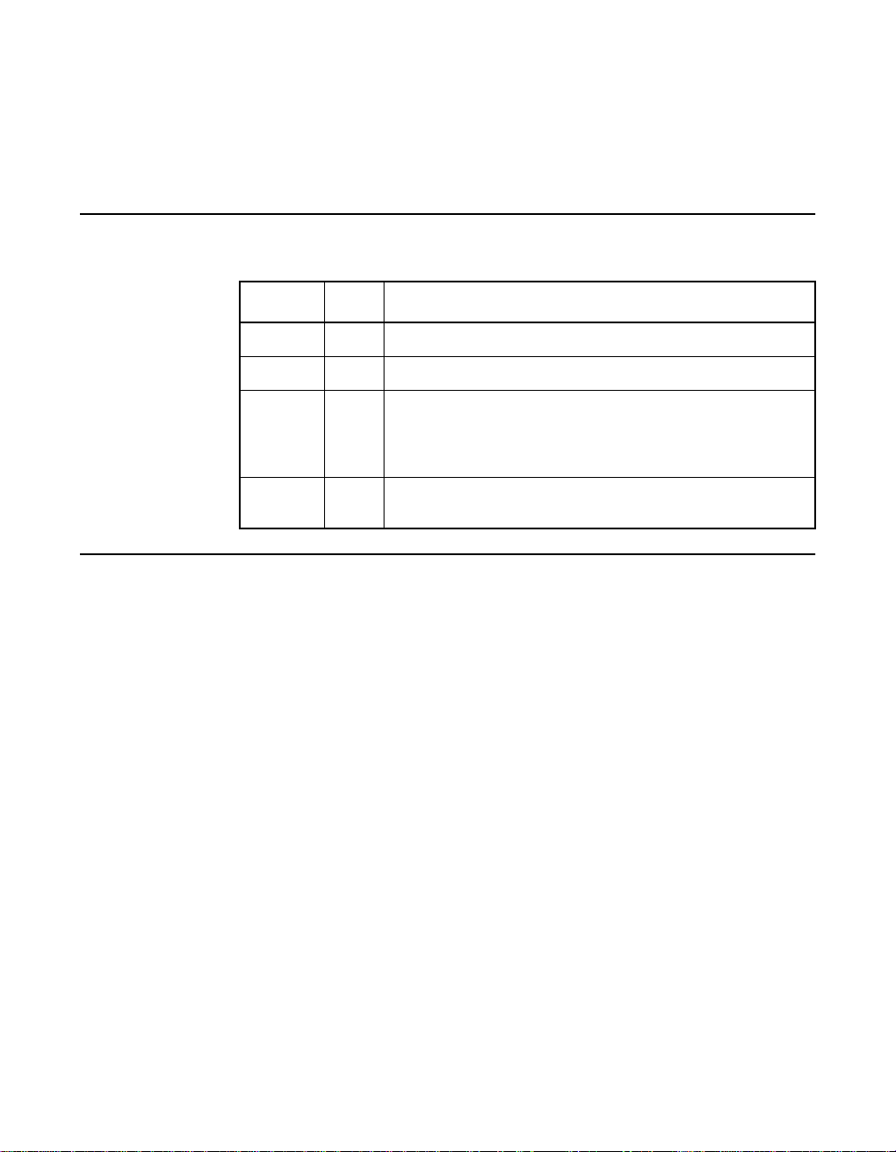
1.1 LSI53C140 SCSI Bus Modes 1-2
1.2 LSI53C140 SCSI Bus Modes 1-2
1.3 LSI53C140 Server Clustering 1-4
1.4 LSI53C140 SCSI Bus Device 1-5
2.1 LSI53C140 Block Diagram 2-2
2.2 LSI53C140 Signal Grouping 2-7
3.1 LSI53C140 160-Pin PQFP Pin Diagram 3-3
3.2 LSI53C140 192-Ball PBGA Top View 3-4
3.3 LSI53C140 Functional Signal Grouping 3-6
3.4 LVD Driver 3-13
3.5 LVD Receiver 3-13
3.6 External Reset Circuit 3-15
3.7 Rise and Fall Time Test Conditions 3-19
3.8 SCSI Input Filtering 3-19
3.9 Hysteresis of SCSI Receivers 3-19
3.10 Input Current as a Function of Input Voltage 3-20
3.11 Output Current as a Function of Output Voltage 3-20
3.12 Clock Timing 3-21
3.13 Input/Output Timing 3-22
3.14 LSI53C140 160-Pin PQFP (PF) Mechanical Drawing 3-24
3.15 192-Ball PBGA (IJ, I2) Mechanical Drawing 3-26
A.1 LSI53C140 Wiring Diagram 1 of 4 A-2
A.2 LSI53C140 Differential Wiring Diagram A-6
Ver. 2.1 Copyright © 1998–2001 by LSI Logic Corporation. All rights reserved.
vii
Page 8

viii
Ver. 2.1 Copyright © 1998–2001 by LSI Logic Corporation. All rights reserved.
Page 9

Tables
1.1 Types of Operation 1-3
1.2 SCSI Bus Distance Requirements 1-5
1.3 Transmission Mode Distance Requirements 1-6
2.1 DIFFSENS Voltage Levels 2-5
2.2 Direction Control Signal Polarity 2-12
2.3 HVD_MODE Control Signal Polarities 2-12
2.4 Mode Sense Control Voltage Levels 2-13
2.5 RESET/ Control Signal Polarity 2-13
2.6 WS_ENABLE/ Signal Polarity 2-14
2.7 XFER_ACTIVE Signal Polarity 2-14
3.1 SCSI A Side Interface Pins 3-7
3.2 SCSI B Side Interface Pins 3-8
3.3 Chip Interface Control Pins 3-9
3.4 Power and Ground Pins 3-10
3.5 Absolute Maximum Stress Ratings 3-11
3.6 Operating Conditions 3-12
3.7 LVD Driver SCSI Signals—A_SD[15:0]±, A_SDP[1:0]±,
A_SCD, A_SIO±, A_SMSG±, A_SREQ±, A_SACK±,
A_SBSY±, A_SATN±, A_SSEL±, A_SRST±, B_SD[15:0]±,
B_SDP[1:0]±, B_SCD, B_SIO±, B_SMSG±, B_SREQ±,
B_SACK±, B_SBSY±, B_SATN±, B_SSEL±, B_SRST± 3-12
3.8 LVD Receiver SCSI Signals—A_SD[15:0]±, A_SDP[1:0]±,
A_SCD±, A_SIO±, A_SMSG±, A_SREQ±, A_SACK±,
A_SBSY±, A_SATN±, A_SSEL±, A_SRST±, B_SD[15:0]±,
B_SDP[1:0]±, B_SCD±, B_SIO±, B_SMSG±, B_SREQ±,
B_SACK±, B_SBSY±, B_SATN±, B_SSEL±, B_SRST± 3-13
3.9 DIFFSENS SCSI Signal 3-14
3.10 Input Capacitance 3-14
3.11 Bidirectional SCSI Signals—A_SD[15:0]±, A_SDP[1:0]±,
A_SREQ±, A_SACK±, B_SD[15:0]±, B_SDP[1:0]±,
B_SREQ±, B_SACK± 3−14
3.12 Bidirectional SCSI Signals—A_SCD, A_SIO±, A_SMSG±,
A_SBSY±, A_SATN±, A_SSEL±, A_SRST±, B_SCD±,
B_SIO±, B_SMSG, B_SBSY±, B_SATN, B_SSEL±,
B_SRST 3-15
3.13 Input Control Signals—CLOCK, RESET/, WS_ENABLE 3-15
3.14 Output Control Signals—BSY_LED, XFER_ACTIVE 3-16
Ver. 2.1 Copyright © 1998–2001 by LSI Logic Corporation. All rights reserved.
ix
Page 10

3.15 TolerANT Technology Electrical Characteristics 3-17
3.16 Clock Timing 3-21
3.17 Input Timing 3-21
3.18 Output Timing 3-22
B.1 Pin Adjustments B-1
B.2 No Connect Pins B-2
x
Ver. 2.1 Copyright © 1998–2001 by LSI Logic Corporation. All rights reserved.
Page 11

Chapter 1
Using the LSI53C140
This chapter describes the LSI53C140 Ultra2 SCSI Bus Expander and
its applications. It includes these topics:
• Section 1.1, “General Description,” page 1-1
• Section 1.2, “Applications,” page 1-3
• Section 1.3, “Benefits of LVDlink,” page 1-7
1.1 General Description
The LSI53C140 is a single chip solution allowing the extension of SCSI
device connectivity and/or cable length limits. A SCSI bus expander
couples bus segments together without any impact to the SCSI protocol,
software, or firmware. The LSI53C140 connects Single-Ended (SE) Ultra,
Low Voltage Differential (LVD) Ultra2, or High Voltage Differential (HVD)
peripherals together in any combination.
The LSI53C140 is capable of supporting any combination of bus mode
SE, HVD, or LVD on either the A or B Side port. This provides the system
designer with maximum flexibility in designing SCSI backplanes to
accommodate any SCSI bus mode.
Figure 1.1 shows the three SCSI bus modes available on the A or B
Side. LVDlink™transceivers provide the multimode LVD, SE, or HVD
capability.
LSI53C140 Ultra2 SCSI Bus Expander 1-1
Ver. 2.1 Copyright © 1998–2001 by LSI Logic Corporation. All rights reserved.
Page 12
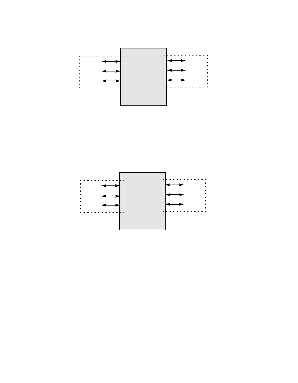
Figure 1.1 LSI53C140 SCSI Bus Modes
A-Side B-Side
LVD
HVD (*)
SE
* All HVD requires external differential transceivers and terminations.
LSI53C140
SCSI Expander
160 PQFP
LVD
HVD (*)
SE
The LSI53C140 is also capable of supporting any combination of SE or
LVD bus mode on either the A or B Side port when using a 192-ball
Plastic Ball Grid Array (PBGA) package. Figure 1.1 illustrates the three
SCSI bus modes available on the A or B Side.
Figure 1.2 LSI53C140 SCSI Bus Modes
A Side B Side
LVD
HVD (*)
SE
LSI53C140
SCSI Expander
192 PBGA
LVD
HVD (*)
SE
* All HVD requires external differential transceivers and terminations.
Refer to the Board Design Considerations in Appendix B about the
LSI53C140 to LSI53C180 as a drop in replacement along with board
design information.
The LSI53C140 operates as both an expander and converter. In both
SCSI bus expander and converter modes, cable segments are
electrically isolated from each other. This feature maintains the signal
integrity of each cable segment.
1-2 Using the LSI53C140
Ver. 2.1 Copyright © 1998–2001 by LSI Logic Corporation. All rights reserved.
Page 13
Table 1.1 shows the types of operations for the LSI53C140 160 Plastic
Quad Flat Pack (PQFP).
Table 1.1 Types of Operation
Signal Type Mode Speed
LVD to LVD Repeater Ultra2
HVD to HVD
SE to SE Repeater Ultra
Or any combination above for Repeater.
LVD to HVD
LVD to SE Converter Ultra
1
HVD
Or any combination above for Converter.
1. All HVD requires external differential transceivers and terminations.
1
1
to SE Converter Ultra
Repeater Ultra
Converter Ultra
The LSI53C140 provides additional control capability through the pin
level isolation mode (Warm Swap Enable). This feature permits logical
disconnection of both the A Side bus and the B Side bus without
disrupting SCSI transfers currently in progress. For example, devices on
the logically disconnected B Side can be swapped out while the A Side
bus remains active.
The LSI53C140 is based on previous bus expander technology resulting
in some signal filtering and retiming to maintain signal skew budgets. The
LSI53C140 is independent of software.
1.2 Applications
The LSI53C140 supports these applications:
• Server clustering environments
• Expanders creating distinct SCSI cable segments which are
Applications 1-3
Ver. 2.1 Copyright © 1998–2001 by LSI Logic Corporation. All rights reserved.
electrically isolated from each other
Page 14
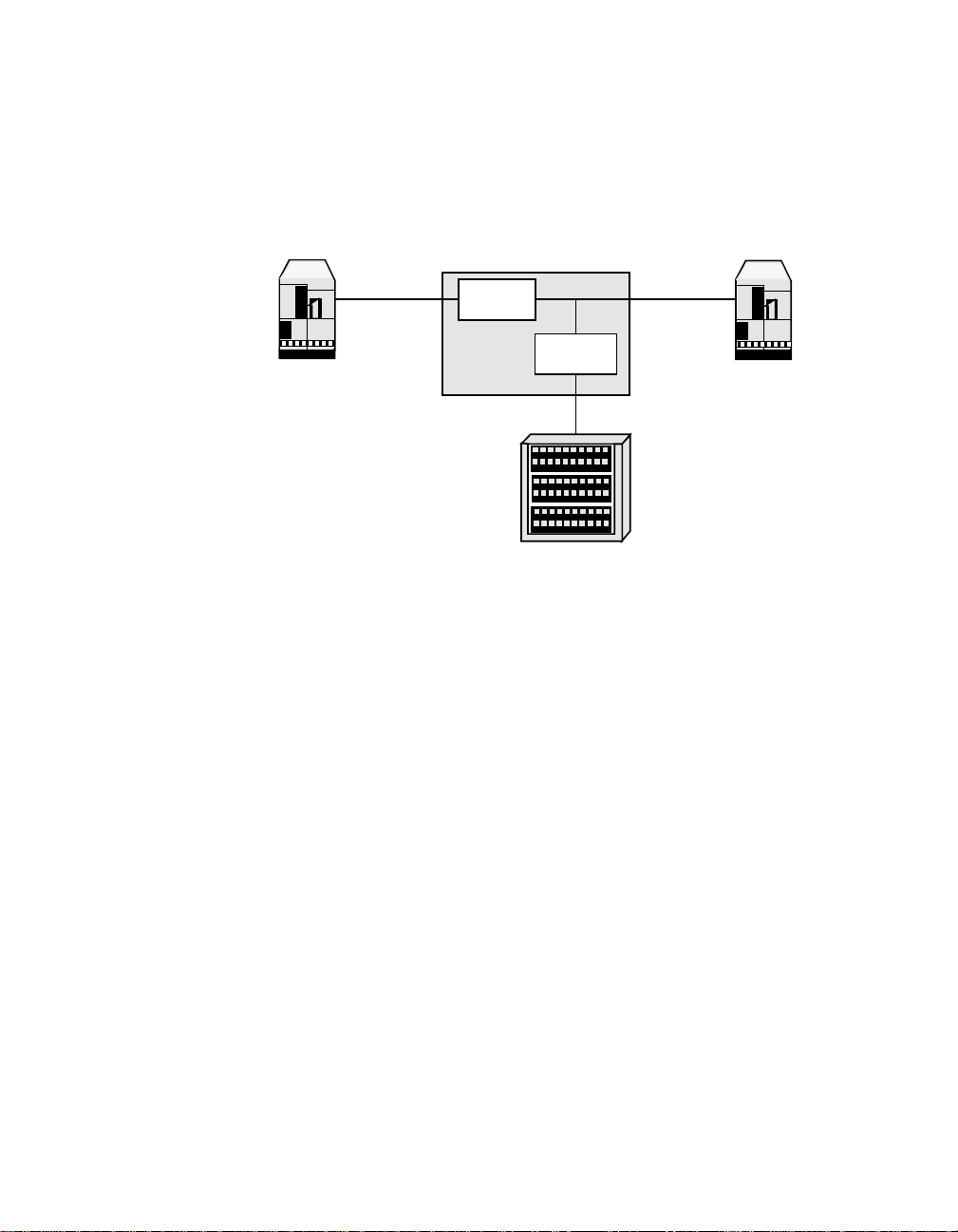
Figure 1.3 shows two LSI53C140 expanders that configure three
segments. This configuration allows segments A and B to be treated as
a point-to-point segment. Segment C is treated as a load segment with
at least 8 inches between every node.
Figure 1.3 LSI53C140 Server Clustering
Primary Server
Segment A
SCSI Bus
Expander
SCSI Bus
Expander
Segment C
Shared Disk Subsystem
Segment B
Secondary Server
Figure 1.3 demonstrates how SCSI bus expanders are used to couple
bus segments together without any impact of the SCSI protocol or
software. Configurations that use the LSI53C140 in the Ultra2 mode
(LVD to LVD) allow the system designer to take advantage of the inherent
cable distance, device connectivity, data reliability, and increased transfer
rate benefits of LVD signaling with Ultra2 SCSI peripherals.
Table 1.2 shows the various distance requirements for each SCSI bus
mode.
1-4 Using the LSI53C140
Ver. 2.1 Copyright © 1998–2001 by LSI Logic Corporation. All rights reserved.
Page 15
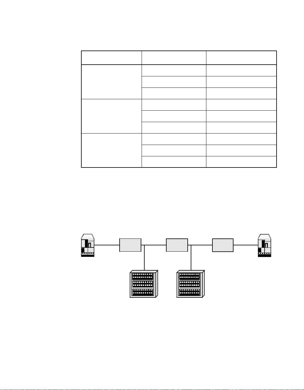
Table 1.2 SCSI Bus Distance Requirements
Segment Mode Length Limit
A LVD (Ultra2) 25 meters
SE (Ultra) 3 meters
1
HVD (Ultra) 25 meters
B LVD (Ultra2) 12 meters
SE (Ultra) 1.5 meters
HVD (Ultra 12 meters
C LVD (Ultra2) 12 meters
SE (Ultra) 1.5 meters
HVD (Ultra) 12 meters
1. The length may be more, possibly 6 meters, as no devices are attached to it.
Figure 1.4 illustrates the cascading of the LSI53C140 to achieve four
distinct SCSI segments. Segments A and D can be treated as point-topoint segments. Segments B and C are treated as load segments with
at least 8-inch spacing between every node.
Figure 1.4 LSI53C140 SCSI Bus Device
Segment A Segment B Segment C
Primary
Server
SCSI Bus
Expander
Shared Disk
Subsystem
SCSI Bus
Expander
Shared Disk
Subsystem
SCSI Bus
Expander
Applications 1-5
Ver. 2.1 Copyright © 1998–2001 by LSI Logic Corporation. All rights reserved.
Segment D
Secondary
Server
Page 16
1.2.1 Features
Table 1.3 shows the various distance requirements for each transmission
mode.
Table 1.3 Transmission Mode Distance Requirements
Segment Mode Length Limit
A, D LVD (Ultra2) 25 meters
SE (Ultra) 1.5 meters
HVD (Ultra) 25 meters
B, C LVD (Ultra2) 12 meters
SE (Ultra) 1.5 meters
HVD (Ultra) 12 meters
The LSI53C140 supports these features:
• Any combination of LVD, SE, or HVD transceivers
• Creates distinct SCSI bus segments that are electrically isolated
from each other
• Integrated LVDlink transceivers for direct attachment to either LVD,
SE, or HVD bus segments
• Operates as a SCSI Bus Expander
– LVD to LVD (Ultra2 SCSI)
– HVD to HVD (Ultra SCSI)
– SE to SE (Ultra SCSI)
• Operates as a SCSI Bus Converter
– LVD to HVD (Ultra SCSI)
– LVD to SE (Ultra SCSI)
– HVD to SE (Ultra SCSI)
• Targets and initiators may be located on either the A or B Side of the
device
1-6 Using the LSI53C140
Ver. 2.1 Copyright © 1998–2001 by LSI Logic Corporation. All rights reserved.
Page 17

• Accepts any asynchronous or synchronous transfer speed up to
Ultra2 SCSI (for LVD to LVD mode only)
• Dynamic addition/removal of SCSI bus segments by using the
electrical isolation mode
• Does not consume a SCSI ID
• Propagates the RESET/ signal from one side to the other regardless
of the SCSI bus state
• Notifies initiator(s) of changes in transmission mode (SE/LVD/HVD)
on A or B side segments by using SCSI bus RESET/
• SCSI Busy LED driver for activity indicator
• Up to four LSI53C140s may be cascaded
• Does not require software
1.2.2 Specifications
The LSI53C140 specifications are:
• 40 MHz Input Clock
• 160-pin PQFP
• 192-ball PBGA; This package is a drop in replacement for the
LSI53C180 when the design uses the LSI53C180 pinout.
• Compliant with the SCSI Parallel Interface (SPI-2)
• Compliant with SCSI Enhanced Parallel Interface (EPI)
Specifications
1.3 Benefits of LVDlink
The LSI53C140 supports LVD technology for SCSI, a signaling
technology that increases the reliability of SCSI data transfers over
longer distances than those supported by SE SCSI technology. The low
current output of LVD allows the I/O transceivers to be integrated directly
onto the chip. LVD provides the reliability of HVD SCSI technology
without the added cost of external differential transceivers. LVD allows a
longer SCSI cable and more devices on the bus. LVD provides a
long-term migration path to even faster SCSI transfer rates without
compromising signal integrity, cable length, or connectivity.
Benefits of LVDlink 1-7
Ver. 2.1 Copyright © 1998–2001 by LSI Logic Corporation. All rights reserved.
Page 18

For backward compatibility to existing SE devices, the LSI53C140
features multimode LVDlink transceivers that can switch between LVD
and SE modes.
Some features of integrated LVDlink Multimode transceivers are:
• Supports SE, LVD, or HVD technology (HVD must have external
transceivers)
• Allows greater device connectivity and longer cable length
• LVDlink transceivers save the cost of external differential transceivers
• Supports a long-term performance migration path
1-8 Using the LSI53C140
Ver. 2.1 Copyright © 1998–2001 by LSI Logic Corporation. All rights reserved.
Page 19

Chapter 2
Functional
Descriptions
This chapter describes all signals, their groupings, and their functions. It
includes these topics:
• Section 2.1, “Interface Signal Descriptions,” page 2-1
• Section 2.2, “SCSI Signal Descriptions,” page 2-6
2.1 Interface Signal Descriptions
The LSI53C140 has no programmable registers, and therefore, no
software requirements. SCSI control signals control all LSI53C140
functions. Figure 2.1 shows a block diagram of the LSI53C140 device
divided into the following blocks:
• A Side SCSI Control Block
– LVD, SE, and HVD drivers and receivers
• B Side SCSI Control Block
– LVD, SE, and HVD drivers and receivers
• Retiming Logic
• Precision Delay Control
• State Machine Control
LSI53C140 Ultra2 SCSI Bus Expander 2-1
Ver. 2.1 Copyright © 1998–2001 by LSI Logic Corporation. All rights reserved.
Page 20
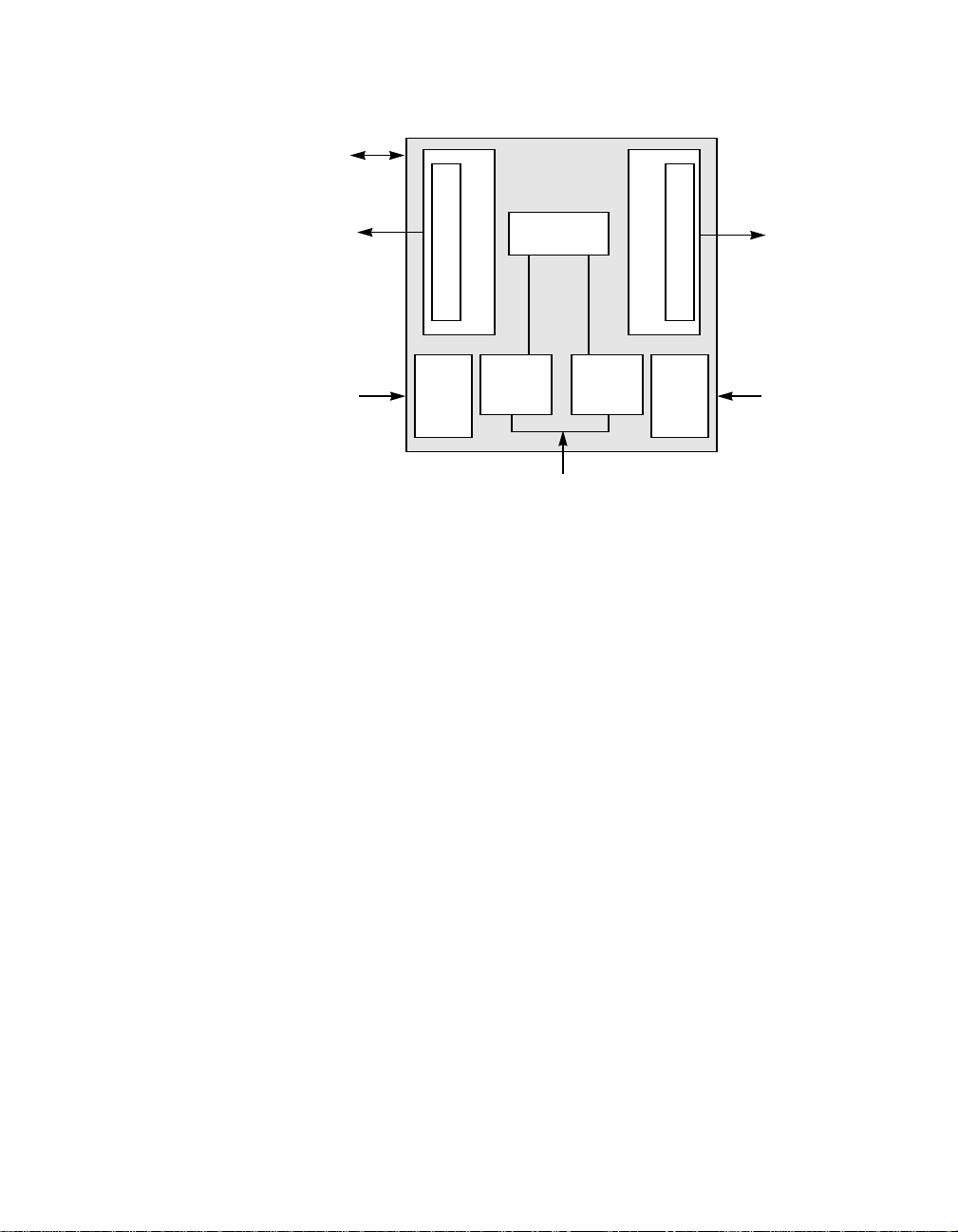
Figure 2.1 LSI53C140 Block Diagram
Control
Signals
LVD, SE, HVD
Wide Ultra SCSI Bus
(A Side)
ansceivers
r
VDink T
L
ol Block
SCSI Contr
Retiming
Logic
k
ol Bloc
LVDink Transceivers
SCSI Contr
LVD, SE, HVD
Wide Ultra SCSI Bus
(B Side)
Precision
er
A_DIFFSENS B_DIFFSENS
VD
L
Control
Receiv
DIFFSENS
Delay
40 MHz Clock Input
In its simplest form, the LSI53C140 passes data and parity from a source
bus to a load bus. The side asserting, deasserting, or releasing the SCSI
signals is the source side. This model of the LSI53C140 represents
pieces of wire that allow corresponding SCSI signals to flow from one
side to the other side. The LSI53C140 monitors arbitration and selection
by devices on the bus so it can enable the proper drivers to pass the
signals along. In addition, the LSI53C140 does signal retiming to
maintain the signal skew budget from the source bus to the load bus.
2.1.1 SCSI A Side and B Side Control Blocks
The SCSI A Side pins are connected internally to the corresponding
SCSI B Side pins, forming bidirectional connections to the SCSI bus.
In the LVD/LVD mode, the SCSI A Side and B Side control blocks
connect to both targets and initiators and accept any asynchronous or
synchronous data transfer rates up to the 80 Mbytes/s rate of Wide
Ultra2 SCSI. TolerANT®and LVDlink technologies are part of both the A
Side and B Side control blocks.
State
Machine
Control
LVD
Receiver
DIFFSENS
2-2 Functional Descriptions
Ver. 2.1 Copyright © 1998–2001 by LSI Logic Corporation. All rights reserved.
Page 21

2.1.1.1 LSI53C140 Requirements for Synchronous Negotiation
The LSI53C140 builds a table of information regarding devices on the
bus in on-chip RAM. The Synchronous Data Transfer Request (SDTR)
and Wide Data Transfer Request (WDTR) information for each device is
taken from the MSG bytes during negotiation. For all devices in the
configuration to communicate accurately with each other through the
LSI53C140 at Ultra2 (Fast-40) rates, it is necessary for a complete
synchronous negotiation to take place between the initiator and target(s)
prior to any data transfer. On a 16-bit bus, the LSI53C140 at Ultra2
approaches rates of 80 Mbytes/s. The LSI53C140 defaults to Fast-20
rates when a valid negotiation between the initiator and target has not
occurred.
2.1.1.2 TolerANT Technology
In the SE mode, the LSI53C140 features TolerANT technology, which
includes active negation on the SCSI drivers and input signal filtering on
the SCSI receivers. Active negation causes the SCSI Request,
Acknowledge, Data, and Parity signals to be actively driven HIGH rather
than passively pulled up by terminators.
TolerANT receiver technology improves data integrity in unreliable
cabling environments, where other devices would be subject to data
corruption. TolerANT receivers filter the SCSI bus signals to eliminate
unwanted transitions without the long signal delays associated with
RC-type input filters. This improved driver and receiver technology helps
eliminate double clocking of data, which is the single biggest reliability
issue with SCSI operations.
The benefits of TolerANT technology include increased immunity to noise
on the deasserting signal edge, better performance due to balanced duty
cycles, and improved SCSI transfer rates. In addition, TolerANT SCSI
devices prevent glitches on the SCSI bus at power-up or power-down, so
other devices on the bus are also protected from data corruption.
Interface Signal Descriptions 2-3
Ver. 2.1 Copyright © 1998–2001 by LSI Logic Corporation. All rights reserved.
Page 22

2.1.1.3 LVDlink Technology
To support greater device connectivity and longer SCSI cables, the
LSI53C140 features LVDlink technology, the LSI Logic implementation of
multimode LVD SCSI. LVDlink transceivers provide the inherent reliability
of differential SCSI, and a long-term migration path of faster SCSI
transfer rates.
LVDlink technology is based on current drive. Its low output current
reduces the power needed to drive the SCSI bus. Therefore, the I/O
drivers can be integrated directly onto the chip. This reduces the cost and
complexity compared to traditional (high power) differential designs.
LVDlink lowers the amplitude of noise reflections and allows higher
transmission frequencies.
The LVDlink transceivers in side A and side B operate in the LVD, HVD
(external differential transceivers), or SE modes. The LSI53C140
automatically detects the type of signal connected, based on the voltages
detected by A_DIFFSENS and B_DIFFSENS.
2.1.2 Retiming Logic
As SCSI signals propagate from one side of the LSI53C140 to the other
side, the logic circuits that retime the bus signals process the SCSI
signals, as needed. This guarantees or improves the required SCSI
timings. The State Machine Controls govern the retiming logic that keeps
track of SCSI phases, the location of initiator and target devices, and
various timing functions. In addition, the retiming logic contains
numerous delay elements that are periodically calibrated by the Precision
Delay Control block. This calibration occurs in order to guarantee
specified timing such as output pulse widths, setup and hold times, and
others.
When a synchronous negotiation takes place between devices, a nexus
is formed, and the on-chip RAM stores the corresponding information for
that nexus. This information remains in place until a chip reset, power
down, or renegotiation occurs. This enables the chips to make more
accurate retiming adjustments.
2-4 Functional Descriptions
Ver. 2.1 Copyright © 1998–2001 by LSI Logic Corporation. All rights reserved.
Page 23
2.1.3 Precision Delay Control
The Precision Delay Control block provides calibration information to the
precision delay elements in the retiming logic block in order to maintain
precise timing as signals propagate through the device. As the
LSI53C140 operating conditions (such as voltage and temperature) vary
over time, the Precision Delay Control block periodically updates the
delay settings in the retiming logic to maintain constant and precise
control over bus timing.
2.1.4 State Machine Control
The State Machine Control keeps track of the SCSI bus phase protocol
and other internal operating conditions. This block provides signals to the
retiming logic that identify how to properly handle SCSI bus signal
retiming and protocol, based on observed bus conditions.
2.1.5 DIFFSENS Receiver
The LSI53C140 contains LVD DIFFSENS receivers that detect the
voltage level on the A Side or B Side DIFFSENS lines to inform the
LSI53C140 of the transmission mode being used by the SCSI buses. The
LVD DIFFSENS receivers are capable of detecting the voltage level of
incoming SCSI signals to determine whether it is from an SE, LVD, or
HVD device. A device does not change its present signal driver or
receiver mode based on the DIFFSENS voltage levels unless a new
mode is sensed continuously for at least 100 ms.
Transmission mode detection for SE, LVD, or HVD is accomplished
through the use of the DIFFSENS lines. Table 2.1 shows the voltages on
the DIFFSENS lines and modes they will cause.
Table 2.1 DIFFSENS Voltage Levels
Voltage Mode
−0.35 to +0.5 SE
+0.7 to +1.9 LVD
+2.4 to +5.5 HVD
Interface Signal Descriptions 2-5
Ver. 2.1 Copyright © 1998–2001 by LSI Logic Corporation. All rights reserved.
Page 24

2.1.6 Dynamic Transmission Mode Changes
Any dynamic mode change (SE/LVD/HVD) on a bus segment is
considered to be a significant event that requires the initiator to
determine whether the mode change meets the requirements for that bus
segment.
The LSI53C140 supports dynamic transmission mode changes by
notifying the initiator(s) of changes in transmission mode (SE/LVD/HVD)
on A or B side segments by using SCSI bus RESET. The DIFFSENS line
detects a valid mode switch on the bus segments. After the DIFFSENS
state is present for 100 ms, the LSI53C140 generates a SCSI reset on
the opposite bus from the one that the transmission mode change
occurred on. This reset informs any initiators residing on the opposite
segment about the change in the transmission mode. Then, the
initiator(s) renegotiates synchronous transfer rates with each device on
that segment to ensure that there is a valid bus segment for that mode.
2.2 SCSI Signal Descriptions
Figure 2.2 shows the LSI53C140 signal grouping. A description of the
signal groups follows. For a description of a specific signal, refer to
Section 3.1, “General Description,” in Chapter 3. For information about
signal electrical characteristics, refer to Section 3.2, “Electrical
Characteristics,” in Chapter 3. For SCSI bus signal timing, see
Section 3.2.4, “SCSI Interface Timing,” in Chapter 3.
2-6 Functional Descriptions
Ver. 2.1 Copyright © 1998–2001 by LSI Logic Corporation. All rights reserved.
Page 25
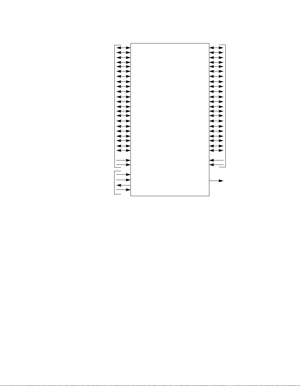
Figure 2.2 LSI53C140 Signal Grouping
A_SSEL+
A_SSEL−
A_SBSY+
A_SBSY−
A-Side
LVD, HVD, or SE
SCSI Interface
Control Signals
A_SRST+
A_SRST−
A_SREQ+
A_SREQ−
A_SACK+
A_SACK−
A_SMSG+
A_SMSG−
A_SCD+
A_SCD−
A_SIO+
A_SIO−
A_SATN+
A_SATN−
A_SDP[1:0]+
A_SDP[1:0]−
A_SD[15:0]+
A_SD[15:0]−
A_DIFFSENS
A_HVD_MODE
RESET/
WS_ENABLE/
XFER_ACTIVE
CLOCK
2.2.1 Data and Parity (SD and SDP)
LSI53C140
B_SSEL+
B_SSEL−
B_SBSY+
B_SBSY−
B_SRST+
B_SRST−
B_SREQ+
B_SREQ−
B_SACK+
B_SACK−
B_SMSG+
B_SMSG−
B_SCD+
B_SCD−
B_SIO+
B_SIO−
B_SATN+
B_SATN−
B_SDP[1:0]+
B_SDP[1:0]−
B_SD[15:0]+
B_SD[15:0]−
B_DIFFSENS
B_HVD_MODE
BSY_LED
B-Side
LVD, HVD, or SE
SCSI Interface
The signals named A_SD[15:0]± and A_SDP[1:0]± are the data and
parity signals from the A Side, and B_SD[15:0]± and B_SDP[1:0]± are
the data and parity signals from the B Side of the LSI53C140. The
LSI53C140 sends and receives these signals by using SCSI compatible
drivers and receiver logic designed into the LSI53C140 interfaces. This
logic provides the multimode LVD and SE interfaces in the chip. This
logic also provides the necessary drive, sense thresholds, and input
hysteresis to function correctly in a SCSI bus environment.
The LSI53C140 receives data and parity signals and passes them from
the source bus to the load bus and provides any necessary edge shifting
to guarantee the skew budget for the load bus. Either side of the
LSI53C140 may be the source bus or the load bus. The side that is
asserting, deasserting, or releasing the SCSI signals is the source side.
These steps describe the LSI53C140 data processing:
SCSI Signal Descriptions 2-7
Ver. 2.1 Copyright © 1998–2001 by LSI Logic Corporation. All rights reserved.
Page 26

1. The receiver logic accepts the asserted data as soon as it is
received. Once the clock signal has been received, data is gated
from the receiver latch.
2. The path is next tested to ensure the signal, if being driven by the
LSI53C140, is not misinterpreted as an incoming signal.
3. The data is then leading edge filtered. The assertion edge is held for
a specified time to prevent any signal bounce. The input signal
controls the duration.
4. The next stage uses a latch to sample the signal. This provides a
stable data window for the load bus.
5. The final step develops pull-up and pull-down controls for the SCSI
I/O logic, including 3-state controls for the pull-up.
6. A parallel function ensures that bus (transmission line) recovery
occurs for a specified time after the last signal deassertion on each
signal line.
2.2.2 SCSI Bus Activity LED (BSY_LED)
Internal logic detects SCSI bus activity and generates a signal that
produces an active HIGH output. This output can be used to drive a LED
to indicate SCSI activity.
The internal circuitry is a digital one shot that is active HIGH with a
minimum pulse width of 16 ms. The BSY_LED output current is 8 mA.
This output may have an LED attached to it with the other lead of the
LED grounded through a suitable resistor.
2.2.3 Select Control (SSEL)
A_SSEL and B_SSEL are control signals used during bus arbitration and
selection. Whichever side asserts, SSEL propagates it to the other side.
If both signals are asserted at the same time, the A Side receives SSEL
and sends it to the B Side. This output has pull-down control for an open
collector driver. The select control signals go through this process:
2-8 Functional Descriptions
Ver. 2.1 Copyright © 1998–2001 by LSI Logic Corporation. All rights reserved.
Page 27

1. The input signal is blocked if it is being driven by the LSI53C140.
2. The next stage is a leading edge filter. This ensures that the output
does not switch for a specified time after the leading edge. The
duration of the input signal then determines the duration of the
output.
3. A parallel function ensures that bus (transmission line) recovery
occurs for a specified time after the last signal deassertion on each
signal line.
2.2.4 Busy Control (SBSY)
A_SBSY and B_SBSY signals are propagated from the source bus to the
load bus. The busy control signals go through this process:
1. The bus is tested to ensure the signal, if being driven by the
LSI53C140, is not misinterpreted as an incoming signal.
2. The data is then leading edge filtered. The assertion edge is held for
a specified time to prevent any signal bounce. The input signal
controls the duration.
3. The signal path switches the long and short filters used in the circuit
depending upon the current state of the LSI53C140. The current
state of the LSI53C140 State Machine that tracks SCSI phases
selects the mode. The short filter mode passes data through, while
the long filter mode indicates the bus free state. When the Busy
(SBSY) and Select (SSEL) sources switch from side to side, the long
filter mode is used. This output is then fed to the output driver, which
is a pull-down open collector only.
4. A parallel function ensures that bus (transmission line) recovery is
availablefor a specified time after the last signal deassertion on each
signal line.
2.2.5 Reset Control (SRST)
The controller passes the A_SRST and B_SRST signals from the source
bus to the load bus. This output has pull-down control for an open
collector driver. The controller processes these reset signals in this
sequence:
SCSI Signal Descriptions 2-9
Ver. 2.1 Copyright © 1998–2001 by LSI Logic Corporation. All rights reserved.
Page 28

1. The input signal is blocked if it is already being driven by the
LSI53C140.
2. The next stage is a leading edge filter. This ensures that the output
does not switch during a specified time after the leading edge. The
duration of the input signal then determines the duration of the
output.
3. A parallel function ensures that bus (transmission line) recovery
occurs for a specified time after the last signal deassertion on each
signal line.
When the LSI53C140 senses a true mode change on either bus, it
generates a SCSI reset to the opposite bus. For example, when LVD
mode changes to SE mode, a reset occurs.
2.2.6 Request and Acknowledge Control (SREQ and SACK)
The A_SREQ, A_SACK, B_SREQ, and B_SACK are clock and control
signals. Their signal paths contain controls to guarantee minimum pulse
widths, filter edges, and does some retiming when used as data transfer
clocks. Only the leading edge is filtered in single transition clocking.
SREQ and SACK have paths from the A Side to the B Side and from the
B Side to the A Side. The received signal goes through these processing
steps before being sent to the opposite bus:
1. The asserted input signal is sensed and forwarded to the next stage
if the direction control permits it. State machines develop the
direction controls that are driven by the sequence of bus control
signals.
2. The signal must then pass the test of not being generated by the
LSI53C140.
3. The next stage is a leading edge filter. This ensures that the output
does not switch during the specified hold time after the leading edge.
The duration of the input signal determines the duration of the output
after the hold time. The circuit guarantees a minimum pulse rate.
4. The next stage passes the signal if it is not a data clock. If SREQ or
SACK is a data clock, it delays the leading edge to improve data
output setup times. The input signal again controls the duration.
2-10 Functional Descriptions
Ver. 2.1 Copyright © 1998–2001 by LSI Logic Corporation. All rights reserved.
Page 29

5. This stage is a trailing edge signal filter. When the signal deasserts,
the filter does not permit any signal bounce. The output signal
deasserts at the first deasserted edge of the input signal.
6. The last stage develops pull-up and pull-down signals with drive and
3-state control.
7. A parallel function ensures that bus (transmission line) recovery
occurs for a specified time after the last signal deassertion on each
signal line.
2.2.7 Control/Data, Input/Output, Message, and Attention Controls (SCD, SIO, SMSG, and SATN)
A_SCD, A_SIO, A_SMSG, A_SATN, B_SCD, B_SIO, B_SMSG, and
B_SATN are control signals that follow these processing steps:
1. The input signal is blocked if it is being driven by the LSI53C140.
2. The next stage is a leading edge filter. This ensures the output does
not switch for a specified time after the leading edge. The duration
of the input signal determines the duration of the output.
3. The final stage develops pull-up and pull-down controls for the SCSI
I/O logic, including 3-state controls for the pull-up.
4. A parallel function ensures that bus (transmission line) recovery is for
a specified time after the last signal deassertion on each signal line.
2.2.8 Differential Direction Control
A_SD[15:0], A_SDP[1:0], A_SBSY, A_SSEL, A_SCD, A_SIO, A_SMSG,
A_SREQ, A_SACK, A_SATN, A_SRST, B_SD[15:0], B_SDP[1:0],
B_SBSY, B_SSEL, B_SCD, B_SIO, B_SMSG, B_SREQ, B_SACK,
B_SATN, and B_SRST are all multimode signals. The HVD_MODE input
pins control the mode and the voltage is sensed at the DIFFSENS inputs.
When the system selects HVD signaling and the DIFFSENS line sees
the proper voltage input, all the minus signal leads become SE
inputs/outputs to HVD drivers/receivers. All plus signals become the HVD
driver/receiver direction control signals. The A and B Sides are
independently controlled. Table 2.2 describes the Direction Control signal
polarity.
SCSI Signal Descriptions 2-11
Ver. 2.1 Copyright © 1998–2001 by LSI Logic Corporation. All rights reserved.
Page 30

Table 2.2 Direction Control Signal Polarity
Signal Level State Effect
LOW = 0 Deasserted Input signals into the LSI53C140.
HIGH = 1 Asserted Drive the LSI53C140 signals onto the bus.
When the system selects SE mode due to the lack of HVD_MODE and
the correct DIFFSENS voltage, the plus signal leads are internally tied to
ground and the minus SCSI signals become the SE input/outputs.
When the system selects LVD mode due to the lack of HVD_MODE and
the correct DIFFSENS voltage, the plus and minus signal leads are
differential signal pairs.
2.2.9 A and B HVD Mode (A_HVD_MODE and B_HVD_MODE)
These inputs inform the LSI53C140 that external drivers and receivers
are used in this particular application. The effect of this control is to
disable the LVDand SE modes of operation from the corresponding port.
Table 2.3 describes the HVD_MODE Control signal polarity.
Table 2.3 HVD_MODE Control Signal Polarities
Signal Level State Effect
LOW = 0 Deasserted LSI53C140 drivers function in SE or LVD mode.
HIGH = 1 Asserted HVD signals and controls are enabled from the
port.
2.2.10 A and B Differential Sense (A_DIFFSENS and B_DIFFSENS)
These control pins determine the mode of SCSI bus signaling that is
expected. Table 2.4 describes the Mode Sense Control voltage levels.
2-12 Functional Descriptions
Ver. 2.1 Copyright © 1998–2001 by LSI Logic Corporation. All rights reserved.
Page 31

Table 2.4 Mode Sense Control Voltage Levels
Voltage Mode
−0.35 to +0.5 SE
+0.7 to +1.9 LVD
+2.4 to +5.5 HVD
For example, if a differential source is plugged into the B Side that has
been configured to run in the differential mode and if a SE source is
detected, then the B Side is disabled and no B Side signals are driven.
This is a protection mechanism for SE interfaces that are connected to
differential drivers.
2.2.11 Control Signals
This section provides information about RESET/, WS_ENABLE, and
XFER_ACTIVE pins. It also describes the function of the CLOCK input.
2.2.11.1 Chip Reset (RESET/)
This general purpose chip reset forces all of the internal elements of the
LSI53C140 into a known state. It brings the State Machine to an idle
state and forces all controls to a passive state. The minimum RESET/
input asserted pulse width is 100 ns.
The LSI53C140 also contains an internal Power On Reset (POR)
function that is ORed with the chip reset pin. This eliminates the need
for an external chip reset if the power supply meets ramp up
specifications. Table 2.5 describes the RESET/ Control signal polarity.
Table 2.5 RESET/ Control Signal Polarity
Signal Level State Effect
LOW = 0 Asserted The chip forces reset to all internal LSI53C140
HIGH = 1 Deasserted LSI53C140 is not in a forced reset state.
SCSI Signal Descriptions 2-13
Ver. 2.1 Copyright © 1998–2001 by LSI Logic Corporation. All rights reserved.
elements.
Page 32

2.2.11.2 Warm Swap Enable (WS_ENABLE/)
This input removes the chip from an active bus without disturbing the
current SCSI transaction (for Warm Swap). When the WS_ENABLE/ pin
is asserted, after detection of the next bus free state, the SCSI signals
are 3-stated. This occurs so that the LSI53C140 no longer passes
through signals until the WS_ENABLE/ pin is deasserted HIGH and both
SCSI buses enter the Bus Free state. As an indication that the chip is
idle, or ready to be warm swapped, the XFER_ACTIVE signal deasserts
LOW. An LED or some other indicator could be connected to the
XFER_ACTIVE signal. This feature of Warm Swap Enable is to isolate
buses in certain situations. Table 2.6 describes the WS_ENABLE/ signal
polarity.
Table 2.6 WS_ENABLE/ Signal Polarity
Signal Level State Effect
LOW = 0 Asserted Requests the LSI53C140 to go off-line after
HIGH = 1 Deasserted Enables the LSI53C140 to run normally.
2.2.11.3 Transfer Active (XFER_ACTIVE)
This output is an indication that the chip has finished its internal testing,
the SCSI bus has entered a Bus Free state, and SCSI traffic can now
pass from one bus to the other. The signal is asserted HIGH when the
chip is active. Table 2.7 describes the XFER_ACTIVE signal polarity.
Table 2.7 XFER_ACTIVE Signal Polarity
Signal Level State Effect
HIGH = 1 Asserted Indicates normal operation, and enables
LOW = 0 Deasserted Detects a Bus Free state by the LSI53C140
detection of a SCSI Bus Free state.
transfers through the LSI53C140.
due to WS_ENABLE/ being low, thus disabling
transfers through the device.
2-14 Functional Descriptions
Ver. 2.1 Copyright © 1998–2001 by LSI Logic Corporation. All rights reserved.
Page 33

2.2.11.4 Clock (CLOCK)
This is the 40 MHz oscillator input to the LSI53C140. It is the clock
source for the protocol control state machines and timing generation
logic. This clock is not used in any bus signal transfer paths.
2.2.12 SCSI Termination
The terminator networks provide the biasing needed to pull signals to an
inactive voltage level, and to match the impedance seen at the end of
the cable with the characteristic impedance of the cable. Terminators
must be installed at the extreme ends of each SCSI segment, and only
at the ends. No SCSI segment should ever have more or less than two
terminators installed and active. SCSI host adapters should provide a
means of accommodating terminators. The terminators should be
socketed, so they may be removed if not needed. Otherwise, the
terminators should be disabled by means of software.
LSI Logic requires the use of multimode terminators because these
terminators provide both LVD and SE termination, depending on what
mode of operation is detected by the DIFFSENS pins. HVD requires a
different termination configuration. The use of active termination is highly
recommended.
SCSI Signal Descriptions 2-15
Ver. 2.1 Copyright © 1998–2001 by LSI Logic Corporation. All rights reserved.
Page 34

2-16 Functional Descriptions
Ver. 2.1 Copyright © 1998–2001 by LSI Logic Corporation. All rights reserved.
Page 35

Chapter 3
LSI53C140
Specifications
This chapter provides the electrical characteristics and descriptions
associated with the 160-pin PQFP and the 192-ball PBGA packages for
the LSI53C140. It includes these topics:
• Section 3.1, “General Description,” page 3-2
• Section 3.2, “Electrical Characteristics,” page 3-11
• Section 3.3, “Mechanical Drawings,” page 3-23
LSI53C140 Ultra2 SCSI Bus Expander 3-1
Ver. 2.1 Copyright © 1998–2001 by LSI Logic Corporation. All rights reserved.
Page 36

3.1 General Description
LSI Logic provides two packages for the LSI53C140:
• A 160-pin PQFP package, and
• A 192-ball PBGA package.
Tables 3.1 through 3.4 list the signal descriptions grouped by function:
• SCSI A Side Interface Pins (Table 3.1)
• SCSI B Side Interface Pins (Table 3.2)
• Chip Interface Control Pins (Table 3.3)
• Power and Ground Pins (Table 3.4)
The decoupling capacitor arrangement shown in Figure 3.1 is
recommended to maximize the benefits of the internal split ground
system. Capacitor values should be between 0.01 µF and 0.1 µF.
Figure 3.1 illustrates the 160-pin PQFP diagram.
3-2 LSI53C140 Specifications
Ver. 2.1 Copyright © 1998–2001 by LSI Logic Corporation. All rights reserved.
Page 37

Figure 3.1 LSI53C140 160-Pin PQFP Pin Diagram
B_SD11+
B_SD11−
B_SD10+
B_SD10−
B_SD9+
B_SD9−
VSS
SCSI
B_SD8+
B_SD8−
VDD
SCSI
B_SIO+
B_SIO−
B_SREQ+
B_SREQ−
VSS
SCSI
B_SCD+
B_SCD−
B_SSEL+
B_SSEL−
B_SMSG+
B_SMSG−
VSS
SCSI
VSS
CORE
B_SRST+
B_SRST−
VDD
CORE
VDD
SCSI
B_SACK+
B_SACK−
B_SBSY+
B_SBSY−
VSS
SCSI
B_SATN+
B_SATN−
B_SDP0+
B_SDP0−
VDD
SCSI
RBIAS
B_SD7+
B_SD7−
SCSI
A_SD14+
VSS
A_SD15−
137
136
135
SCSI
A_SD15+
VDD
A_SDP1−
134
133
132
A_SDP1+
A_SD0−
A_SD0+
VSS
131
130
129
128
SCSI
VSS
1
2
3
4
5
6
7
8
9
10
11
12
13
14
15
16
17
18
19
20
21
22
23
24
25
26
27
28
29
30
31
32
33
34
35
36
37
38
39
40
SCSI
B_DIFFSENS
VDDIOB_HVD_MODE
NCNCNCNCNCNCWS_ENABLE/
160
159
158
157
156
155
154
153
152
151
150
XFER_ACTIVE
149
BSY_LED
CLOCK
RESET/
A_HVD_MODE
148
147
146
145
VSSIOA_DIFFSENS
A_SD12−
A_SD12+
A_SD13−
A_SD13+
144
143
142
141
140
139
Top View
A_SD14−
138
414243444546474849505152535455565758596061626364656667686970717273747576777879
A_SD1−
A_SD1+
127
126
A_SD2−
A_SD2+
125
124
A_SD3−
A_SD3+
123
122
SCSI
VDD
121
120
119
118
117
116
115
114
113
112
111
110
109
108
107
106
105
104
103
102
101
100
80
VSS
SCSI
A_SD4−
A_SD4+
A_SD5−
A_SD5+
A_SD6−
A_SD6+
VDD
SCSI
A_SD7−
A_SD7+
VSS
SCSI
A_SDP0−
A_SDP0+
A_SATN−
A_SATN+
A_SBSY−
A_SBSY+
VSS
CORE
VSS
SCSI
A_SACK−
A_SACK+
99
VDD
98
97
96
95
94
93
92
91
90
89
88
87
86
85
84
83
82
81
SCSI
VDD
CORE
A_SRST−
A_SRST+
VSS
SCSI
A_SMSG−
A_SMSG+
A_SSEL−
A_SSEL+
A_SCD−
A_SCD+
VSS
SCSI
A_SREQ−
A_SREQ+
A_SIO−
A_SIO+
A_SD8−
A_SD8+
VDD
SCSI
SCSI
B_SD6−
B_SD5−
B_SD6+
B_SD5+
VSS
B_SD4+
1. NC pins are not connected.
Figure 3.2 illustrates the 192-ball PBGA package.
General Description 3-3
Ver. 2.1 Copyright © 1998–2001 by LSI Logic Corporation. All rights reserved.
B_SD4−
SCSI
B_SD3+
VSS
B_SD3−
SCSI
B_SD2+
VDD
B_SD2−
B_SD1+
B_SD1−
SCSI
B_SD0+
VSS
B_SD0−
B_SDP1+
B_SD15+
B_SDP1−
VSS
B_SD15−
SCSI
B_SD14−
B_SD14+
SCSI
VDD
B_SD13+
B_SD13−
B_SD12+
SCSI
SCSI
SCSI
VSS
VSS
B_SD12−
VDD
A_SD11−
A_SD11+
A_SD9+
A_SD10−
A_SD10+
SCSI
A_SD9−
VSS
Page 38

Figure 3.2 LSI53C140 192-Ball PBGA Top View
A1 A2 A3 A4 A5 A6 A7 A8 A9
NC
B1 B2 B3 B4 B5 B6 B7 B8 B9
B_SD11+ B_SD11- NC NC WS_ENABLE/ BSY_LED A_HVD_MODE
C1 C2 C3 C4 C5 C6 C7 C8 C9
B_SD10+ B_SD10- B_DIFFSENS NC
D1 D2 D3
B_SD9+ B_SD9- NC
E1 E2 E3
B_SD8+ B_SD8-
F1 F2 F3
B_SIO+ B_SIO- NC
G1 G2 G3 G7 G8 G9
B_SREQ+ B_SREQ- VSS VSS VSS VSS
H1 H2 H3 H7 H8 H9
B_SCD- B_SSEL+ B_SCD+ VSS VSS VSS
J1 J2 J3 J7 J8
B_SSEL- B_SMSG+
K1 K2 K3 K7 K8 K9
B_SMSG- B_SRST+
L1 L2 L3 L7 L8 L9
B_SRST- NC VSS VSS VSS VSS
M1 M2 M3
VDD
B_HVD_MODE NC NC XFER_ACTIVE RESET/ A_DIFFSENS A_SD12-
IO
VDD
VDD
VDD
VDD
SCSI
SCSI
CORE
VDD
SCSI
NC VSS CLOCK
VSS VSS
VSS VSS VSS
CORE
A_SD12+
VDD
SCSI
B_SACK+ B_SACK- B_SBSY+
N1 N2 N3
B_SBSY- B_SATN+
P1 P2 P3
B_SATN- B_SDP0- B_SDP0+
R1 R2 R3 R4 R5 R6 R7 R8 R9
RBIAS B_SD7+ B_SD7- NC
T1 T2 T3 T4 T5 T6 T7 T8 T9
NC B_SD6+ B_SD5+ B_SD4+ B_SD3+ B_SD2- B_SD1+ B_SD0+ B_SDP1+
U1 U2 U3 U4 U5 U6 U7 U8 U9
NC B_SD6- B_SD5- B_SD4- B_SD3- NC B_SD1-
VDD
SCSI
VDD
SCSI
B_SD2+ VSS B_SD0-
VDD
CORE
3-4 LSI53C140 Specifications
Ver. 2.1 Copyright © 1998–2001 by LSI Logic Corporation. All rights reserved.
VDD
SCSI
B_SDP1-
Page 39

Figure 3.2 LSI53C140 192-Ball PBGA Top View (Cont.)
A10 A11 A12 A13 A14 A15 A16 A17
A_SD13- A_SD14+ A_SD15+ A_SD0- A_SD1- A_SD2- A_SD3- NC
B10 B11 B12 B13 B14 B15 B16 B17
A_SD14- A_SD15- A_SDP1- A_SD0+ A_SD1+ A_SD2+ A_SD3+ A_SD4-
C10 C11 C12 C13 C14 C15 C16 C17
A_SD13+ VSS A_SDP1+
VDD
SCSI
NC NC A_SD5- A_SD4+
D15 D16 D17
A_SD5+ A_SD6+ A_SD6-
E15 E16 E17
VDD
SCSI
F15 F16 F17
A_SD7+ A_SD7-
G10 G11 G15 G16 G17
VSS VSS VSS A_SATN+ A_SATN-
H10 H11 H15 H16 H17
VSS VSS NC A_SBSY+ A_SBSY-
J10 J11 J15 J16 J17
VSS VSS
K10 K11 K15 K16 K17
VSS VSS
L10 L11 L15 L16 L17
VSS VSS VSS A_SMSG- A_SRST+
R10 R11 R12 R13 R14 R15 R16 R17
NC VSS NC
T10 T11 T12 T13 T14 T15 T16 T17
B_SD15+ B_SD14+ B_SD13+ B_SD12+ A_SD11+ A_SD10- A_SD8+ A_SD8-
U10 U11 U12 U13 U14 U15 U16 U17
VDD
SCSI
A_SD10+ A_SD9- A_SIO+ A_SIO-
NC A_SDP0+ A_SDP0-
VDD
SCSI
VDD
CORE
M15 M16 M17
A_SSEL+ A_SSEL- A_SMSG+
N15 N16 N17
VDD
SCSI
P15 P16 P17
A_SACK+ A_SACK-
A_SRST- NC
A_SCD+ A_SCD-
NC A_SREQ+ A_SREQ-
B_SD15- B_SD14- B_SD13- B_SD12- A_SD11- A_SD9+ NC NC
General Description 3-5
Ver. 2.1 Copyright © 1998–2001 by LSI Logic Corporation. All rights reserved.
Page 40

3.1.1 Signal Descriptions
This section provides the descriptions for the signals associated with the
LSI53C140. Figure 3.3 illustrates the functional signal grouping for the
LSI53C140.
Figure 3.3 LSI53C140 Functional Signal Grouping
A-Side
LVD, HVD, or SE
SCSI Interface
Control Signals
A_SSEL+
A_SSELA_SBSY+
A_SBSYA_SRST+
A_SRSTA_SREQ+
A_SREQA_SACK+
A_SACKA_SMSG+
A_SMSGA_SCD+
A_SCDA_SIO+
A_SIOA_SATN+
A_SATNA_SDP[1:0]+
A_SDP[1:0]A_SD[15:0]+
A_SD[15:0]-
A_DIFFSENS
A_HVD_MODE
RESET/
WS_ENABLE/
XFER_ACTIVE
CLOCK
LSI53C140
B_SSEL+
B_SSEL-
B_SBSY+
B_SBSY-
B_SRST+
B_SRST-
B_SREQ+
B_SREQ-
B_SACK+
B_SACK-
B_SMSG+
B_SMSG-
B_SCD+
B_SCD-
B_SIO+
B_SIO-
B_SATN+
B_SATN-
B_SDP[1:0]+
B_SDP[1:-0]-
B_SD[15:0]+
B_SD[15:0]-
B_DIFFSENS
B_HVD_MODE
BSY_LED
B-Side
LVD, HVD, or SE
SCSI Interface
3-6 LSI53C140 Specifications
Ver. 2.1 Copyright © 1998–2001 by LSI Logic Corporation. All rights reserved.
Page 41

Table 3.1 lists and describes the SCSI A side interface pins for the
LSI53C140.
Table 3.1 SCSI A Side Interface Pins
Name Pin Ball Type Description
A_SSEL+,− 91, 92 M15, M16 I/O A Side SCSI bus Select control signal.
A_SBSY+,− 104, 105 H16, H17 I/O A Side SCSI bus Busy control signal.
A_SRST+,− 96, 97 L17, K16 I/O A Side SCSI bus Reset control signal.
A_SREQ+,− 86, 87 P16, P17 I/O A Side SCSI bus Request control
A_SACK+,− 100, 101 J16, J17 I/O A Side SCSI bus Acknowledge control
A_SMSG+,− 93, 94 M17, L16 I/O A Side SCSI bus Message control
A_SCD+,− 89, 90 N16, N17 I/O A Side SCSI bus Control and Data
A_SIO+,− 84, 85 R16, R17 I/O A Side SCSI bus Input and Output
A_SATN+,− 106, 107 G16, G17 I/O A Side SCSI bus Attention control
A_SDP[1:0]+,− 131, 132, 108,
109
A_SD[15:0]+,− 134, 135, 137,
138, 139, 140
141, 142,
73, 74, 76, 77,
78, 79, 82, 83,
111, 112, 114,
115, 116, 117,
118, 119, 122,
123, 124, 125,
126, 127, 129,
130
C12, B12, F16,
F17
A12, B11, A11,
B10, C10, A10,
B9, A9, T14,
U14, R14, T15,
U15, R15, T16,
T17, E16, E17,
D16, D17, D15,
C16, C17, B17,
B16, A16, B15,
A15, B14, A14,
B13, A13
signal.
signal.
signal.
control signal.
control signal.
signal.
I/O A Side SCSI bus Data Parity signal.
I/O A Side SCSI bus Data signals.
A_DIFFSENS 143 A8 I A Side SCSI bus Differential Sense
A_HVD_MODE 145 B7 I A Side SCSI bus HVD Mode control
General Description 3-7
Ver. 2.1 Copyright © 1998–2001 by LSI Logic Corporation. All rights reserved.
signal.
signal.
Page 42

Table 3.2 lists and describes the SCSI B side interface pins for the
LSI53C140.
Table 3.2 SCSI B Side Interface Pins
Name Pin Ball Type Description
B_SSEL+,− 18, 19 H2, J1 I/O B Side SCSI bus Select control signal.
B_SBSY+,− 30, 31 M3, N1 I/O B Side SCSI bus Busy control signal.
B_SRST+,− 24, 25 K2, L1 I/O B Side SCSI bus Reset control signal.
B_SREQ+,− 13, 14 G1, G2 I/O B Side SCSI bus Request control signal.
B_SACK+,− 28, 29 M1, M2 I/O B Side SCSI bus Acknowledge control
B_SMSG+,− 20, 21 J2, K1 I/O B Side SCSI bus Message control
B_SCD+,− 16, 17 H3, H1 I/O B Side SCSI bus Control and Data
B_SIO+,− 11, 12 F1, F2 I/O B Side SCSI bus Input and Output
B_SATN+,− 33, 34 N2, P1 I/O B Side SCSI bus Attention control signal.
B_SDP[1:0]+,− 59, 60, 35, 36 T9, U9, P3, P2 I/O B Side SCSI bus Data Parity signal.
B_SD[15:0]+,− 61, 62, 64, 65,
67, 68, 69, 70,
1, 2, 3, 4, 5, 6,
8, 9, 39, 40,
42, 43, 44, 45,
46, 47, 49, 50,
52, 53, 54, 55,
57, 58
B_DIFFSENS 159 C3 I B Side SCSI bus Differential Sense
B_HVD_MODE 157 A3 I B Side SCSI bus HVD Mode control
T10, U10, T11,
U11, T12, U12,
T13, U13, B1,
B2, C1, C2,
D1, D2, E1, E2,
R2, R3, T2, U2,
T3, U3, T4, U4,
T5, U5, R6, T6,
T7, U7, T8, R8
signal.
signal.
control signal.
control signal.
I/O B Side SCSI bus Data signals.
signal.
signal.
3-8 LSI53C140 Specifications
Ver. 2.1 Copyright © 1998–2001 by LSI Logic Corporation. All rights reserved.
Page 43

Table 3.3 lists and describes the LSI53C140 interface control pins.
Table 3.3 Chip Interface Control Pins
Name Pin Ball Type Description
RESET/ 146 A7 I Master Reset for LSI53C140, active LOW.
WS_ENABLE/ 150 B5 I Enable/disable SCSI transfers through the
LSI53C140.
XFER_ACTIVE 149 A6 O Transfers through the LSI53C140 are
enabled/disabled.
CLOCK 147 C8 I Oscillator input for LSI53C140 (40 MHz).
BSY_LED 148 B6 O SCSI activity LED output, 8 mA.
General Description 3-9
Ver. 2.1 Copyright © 1998–2001 by LSI Logic Corporation. All rights reserved.
Page 44

Table 3.4 lists and describes the LSI53C140 power and ground pins.
Table 3.4 Power and Ground Pins
Name Pin Ball Type Description
VDD
SCSI
VDD
CORE
VDD
IO
VSS 7, 15, 22, 32, 41,
10, 27, 37, 51, 66,
75,81, 99, 113,121,
133
C5, C9, C13, E3, E15,
J3, J15, N3, N15, R5,
R9, R13
I Power supplies to the SCSI bus
I/O pins.
26, 98 B8, K3, K15, U8 I Power supplies to the CORE
logic.
158 A2 I Power supplies to the I/O logic.
I Ground ring.
48, 56, 63, 71, 72,
80,88, 95, 102,110,
120, 128, 136, 160,
23, 103, 144
C7, C11, G3, G7, G8,
G9, G10, G11, G15,
H7, H8, H9, H10, H11,
J7, J8, J10, J11, K7,
K8, K9, K10, K11, L3,
L7, L8, L9, L10, L11,
L15, R7, R11
RBIAS 38 R1 I Receiver bias control, R =
9.76 kΩ 1%.
NC 151–156 A1, A4, A5, A17, B3,
N/A No Connections.
B4, C4, C6, C14, C15,
D3, F3, F15, H15, K17,
L2, P15, R4, R10, R12,
T1, U1, U6, U16, U17
Notes:
• All V
• If the power supplies to the VDD
either power up the pins simultaneously or power up VDD
always power down before the VDD
pins must be supplied 3.3 V. The LSI53C140 output signals drive 3.3 V.
DD
and VDD
IO
CORE
pins in a chip testing environment are separated,
CORE
before VDDIO. The VDDIOpin must
CORE
pin.
3-10 LSI53C140 Specifications
Ver. 2.1 Copyright © 1998–2001 by LSI Logic Corporation. All rights reserved.
Page 45

3.2 Electrical Characteristics
This section specifies the DC and AC electrical characteristics of the
LSI53C140. These electrical characteristics are in the following four
categories:
• DC Characteristics
• TolerANT Technology Electrical Characteristics
• AC Characteristics
• SCSI Interface Timing
3.2.1 DC Characteristics
Tables 3.5 through 3.14 give the current and voltage specifications.
Figures 3.4 through 3.6 are driver schematics for the LSI53C140.
Table 3.5 Absolute Maximum Stress Ratings
Symbol Parameter Min Max Unit
T
V
V
V
IN5V
I
LP
ESD Electrostatic
1. Stresses beyond those listed above may cause permanent damage to the
device. These are stress ratings only; functional operation of the device at
these or any other conditions beyond those indicated in the Operating
Conditions section of the manual is not implied.
2. This voltage is for the SCSI pins.
3. This voltage is for the remaining pins.
4. − 2 V < VPIN < 8 V.
Storage temperature −55 150 °C–
STG
Supply voltage −0.5 4.5 V –
DD
Input voltage VSS−0.3 7
IN
Input voltage (5 V
TolerANT pins)
4
Latch-up current ±150 – mA –
discharge
VSS−0.3 5.25 V –
– 2 K V MIL-STD 883C,
5.55
1
Test
Conditions
2
V
3
V
–
Method 3015.7
Electrical Characteristics 3-11
Ver. 2.1 Copyright © 1998–2001 by LSI Logic Corporation. All rights reserved.
Page 46

Table 3.6 Operating Conditions
1
Symbol Parameter Min Max Unit Test Conditions
V
I
I
DD-I/O
I
θ
θ
Supply voltage 3.13 3.47 V –
DD
DD
Supply current
(dynamic SE)
Supply current
– 130 mA –
– 600 mA –
(dynamic LVD)
Supply current (static) – 1 mA –
DD
T
Operating free air 0 70 ˚C –
A
2
Thermal resistance
JA
(junction to ambient air)
3
Thermal resistance
JA
(junction to ambient air)
– 35 ˚C/W –
– 20.4 ˚C/W Zero airflow
1. Conditions that exceed the operating limits may cause the device to function
incorrectly.
2. Value for QFP package.
3. Value for BGA package.
Table 3.7 LVD Driver SCSI Signals—A_SD[15:0]±, A_SDP[1:0]±,
A_SCD, A_SIO±, A_SMSG±, A_SREQ±, A_SACK±,
A_SBSY±, A_SATN±, A_SSEL±, A_SRST±, B_SD[15:0]±,
B_SDP[1:0]±, B_SCD, B_SIO±, B_SMSG±, B_SREQ±,
B_SACK±, B_SBSY±, B_SATN±, B_SSEL±, B_SRST±
1
Symbol Parameter Min Max Units Test Conditions
I
+ Source (+) current 7 12 mA Asserted state
O
I
− Sink (−) current −7 −12 mA Asserted state
O
I
+ Source (+) current −3.5 −6 mA Negated state
O
I
− Sink (−) current 3.5 6 mA Negated state
O
I
OZ
3-state leakage −20 20 µAV
1. VCM= 0.7–1.8 V, RL= 0–110 Ω, R
3-12 LSI53C140 Specifications
Ver. 2.1 Copyright © 1998–2001 by LSI Logic Corporation. All rights reserved.
= 9.76 kΩ.
bias
= 0 V, 3.47 V
PIN
Page 47

Figure 3.4 LVD Driver
R
L
+
−
IO+
IO−
2
R
L
2
+
V
CM
−
Table 3.8 LVD Receiver SCSI Signals—A_SD[15:0]±,
A_SDP[1:0]±, A_SCD±, A_SIO±, A_SMSG±, A_SREQ±,
A_SACK±, A_SBSY±, A_SATN±, A_SSEL±, A_SRST±,
B_SD[15:0]±, B_SDP[1:0]±, B_SCD±, B_SIO±,
B_SMSG±, B_SREQ±, B_SACK±, B_SBSY±, B_SATN±,
B_SSEL±, B_SRST±
Symbol Parameter Min Max Units Test Conditions
1
LVD receiver voltage
V
I
asserting
V
LVD receiver voltage negating – −60 mV –
I
1. VCM= 0.7–1.8 V.
Figure 3.5 LVD Receiver
+
V
+
V
CM
−
I
2
−
+
V
I
2
−
+
−
60 – mV –
Electrical Characteristics 3-13
Ver. 2.1 Copyright © 1998–2001 by LSI Logic Corporation. All rights reserved.
Page 48

Table 3.9 DIFFSENS SCSI Signal
Symbol Parameter Min Max Unit Test Conditions
V
V
V
HVD sense voltage 2.4 VDD+0.3 V –
IH
LVD sense voltage 0.7 1.9 V –
S
SE sense voltage VSS−0.3 0.5 V –
IL
I
Input leakage −10 10 µAV
IN
= 0 V, 5.25 V
PIN
Table 3.10 Input Capacitance
Symbol Parameter Min Max Unit
C
Input capacitance of input pads – 7 pF –
I
C
Input capacitance of I/O pads – 10 pF –
IO
Test
Conditions
Table 3.11 Bidirectional SCSI Signals—A_SD[15:0]±, A_SDP[1:0]±,
A_SREQ±, A_SACK±, B_SD[15:0]±, B_SDP[1:0]±,
B_SREQ±, B_SACK±
Symbol Parameter Min Max Unit
V
V
V
V
I
Input high voltage 2.0 VDD+0.3 V –
IH
Input low voltage VSS−0.3 0.8 V –
IL
1
Output high voltage 2.0 V
OH
Output low voltage V
OL
3-state leakage −20 20 µAV
OZ
SS
DD
0.5 V 48 mA
1. TolerANT active negation enabled.
VIOH= 7.0 mA
Test
Conditions
= 0 V, 3.47 V
PIN
3-14 LSI53C140 Specifications
Ver. 2.1 Copyright © 1998–2001 by LSI Logic Corporation. All rights reserved.
Page 49

Table 3.12 Bidirectional SCSI Signals—A_SCD±, A_SIO±,
A_SMSG±, A_SBSY±, A_SATN±, A_SSEL±, A_SRST±,
B_SCD±, B_SIO±, B_SMSG ,B_SBSY±, B_SATN ,
B_SSEL±, B_SRST
Symbol Parameter Min Max Unit Test Conditions
V
V
V
I
Input high voltage 2.0 VDD+0.3 V –
IH
Input low voltage VSS−0.3 0.8 V –
IL
Output low
OL
voltage
3-state leakage −20 20 µAV
OZ
V
SS
0.5 V 48 mA
= 0 V, 3.47 V
PIN
Table 3.13 Input Control Signals—CLOCK, RESET/, WS_ENABLE
Symbol Parameter Min Max Unit Test Conditions
V
V
I
Input high voltage 2.0 5.55
IH
Input low voltage V
IL
Input leakage −10 10 µAV
OZ
SS
1
V–
0.8 V –
= 0 V, 5.25 V
PIN
1. Operating Conditions.
Figure 3.6 External Reset Circuit
3.3 V
3.3 V
Input
0.1 µF
Reset
Pin 146
Electrical Characteristics 3-15
Ver. 2.1 Copyright © 1998–2001 by LSI Logic Corporation. All rights reserved.
Page 50

Table 3.14 Output Control Signals—BSY_LED, XFER_ACTIVE
Symbol Parameter Min Max Unit Test Conditions
V
V
I
Output high voltage 2.4 V
OH
Output low voltage V
OL
3-state leakage –10 10 µAV
OZ
SS
DD
0.4 V 8 mA
V8mA
= 0 V, 5.25 V
PIN
3-16 LSI53C140 Specifications
Ver. 2.1 Copyright © 1998–2001 by LSI Logic Corporation. All rights reserved.
Page 51

3.2.2 TolerANT Technology Electrical Characteristics
The LSI53C140 features TolerANT technology, which includes active
negation on the SCSI drivers and input signal filtering on the SCSI
receivers. Active negation actively drives the SCSI Request,
Acknowledge, Data, and Parity signals HIGH rather than allowing them
to be passively pulled up by terminators. Table 3.15 provides electrical
characteristics for SE SCSI signals. Figures 3.7 through 3.11 provide
reference information for testing SCSI signals.
Table 3.15 TolerANT Technology Electrical Characteristics
1
Symbol Parameter Min Max Units Test Conditions
2
V
OH
V
V
V
V
V
V
V
TH–VTL
I
OH
I
OL
I
OSH
OL
TH
Output high voltage 2.0 VDD+0.3 V IOH= −7mA
Output low voltage V
Input high voltage 2.0 VDD+0.3 V –
IH
Input low voltage VSS–0.3 0.8 V Referenced to V
IL
Input clamp voltage –0.66 –0.77 V VDD= 4.75;
IK
SS
0.5 V IOL=48mA
Threshold, HIGH to LOW 1.0 1.2 V –
Threshold, LOW to HIGH 1.4 1.6 V –
TL
Hysteresis 300 500 mV –
2
Output high current 2.5 24 mA VOH= 2.5 V
Output low current 100 200 mA VOL= 0.5 V
2
Short-circuit output high
– 625 mA Output driving low,
current
I
= −20 mA
I
pin shorted to V
supply
I
OSL
Short-circuit output low
current
– 95 mA Outputdriving high,
pin shorted to V
supply
SS
DD
3
SS
I
LH
(Sheet 1 of 2)
Input high leakage – 20 µAV
V
PIN
5%,
DD
= 2.7 V
Electrical Characteristics 3-17
Ver. 2.1 Copyright © 1998–2001 by LSI Logic Corporation. All rights reserved.
Page 52

Table 3.15 TolerANT Technology Electrical Characteristics1(Cont.)
Symbol Parameter Min Max Units Test Conditions
dV
dV
I
LL
I
PD
R
C
t
R
t
H
L
Input low leakage – –20 µAV
Power down leakage – 20 µAV
Input resistance 20 – MΩ SCSI pins
I
Capacitance per pin – 15 pF PQFP
P
2
Rise time, 10% to 90% 4.0 18.5 ns Figure 3.7
Fall time, 90% to 10% 4.0 18.5 ns Figure 3.7
F
V
V
PIN
DD
PIN
DD
= 1.2 V
±5%
=0V
=0V,
/dt Slew rate, LOW to HIGH 0.15 0.50 V/ns Figure 3.7
/dt Slew rate, HIGH to LOW 0.15 0.50 V/ns Figure 3.7
ESD Electrostatic discharge 2 – kV MIL-STD-883C;
3015-7
Latch-up 100 – mA –
Filter delay 20 30 ns Figure 3.8
Ultra filter delay 10 15 ns Figure 3.8
Ultra2 filter delay 5 8 ns Figure 3.8
Extended filter delay 40 60 ns Figure 3.8
,
4
(Sheet 2 of 2)
1. These values are guaranteed by periodic characterization; they are not 100% tested on every device.
2. Active negation outputs only: Data, Parity, SREQ/, SACK/. (Minus Pins) SCSI mode only.
3. Single pin only; irreversible damage may occur if sustained for more than one second.
4. SCSI RESET/ pin has 10 kΩ pull-up resistor.
3-18 LSI53C140 Specifications
Ver. 2.1 Copyright © 1998–2001 by LSI Logic Corporation. All rights reserved.
Page 53
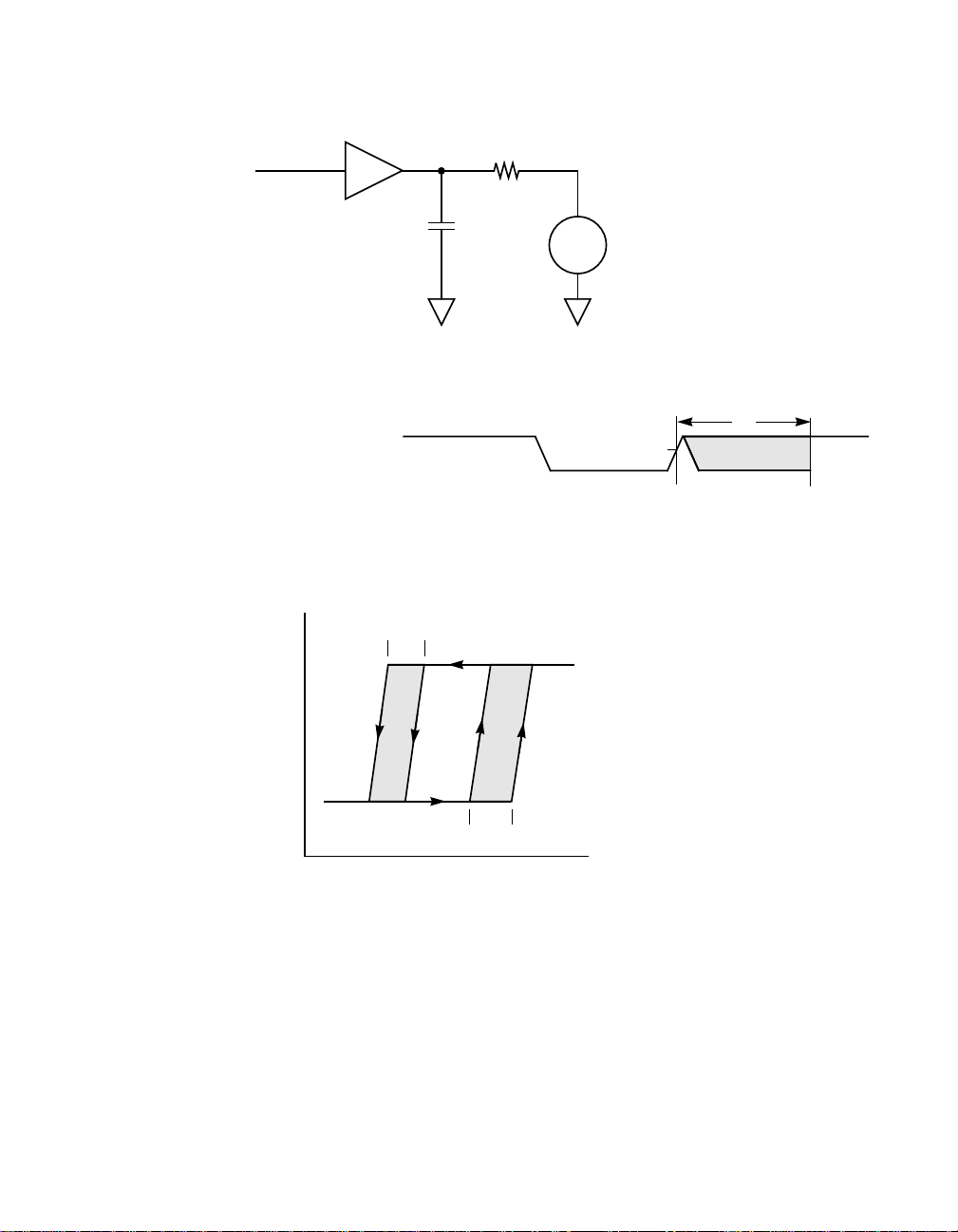
Figure 3.7 Rise and Fall Time Test Conditions
47 Ω
20 pF
+
2.5 V
−
Figure 3.8 SCSI Input Filtering
REQ/ or ACK/ Input
Note: t1is the input filtering period.
Figure 3.9 Hysteresis of SCSI Receivers
1.1 1.3
1
t
V
TH
1
0
Received Logic Level
1.5 1.7
Input Voltage (Volts)
Electrical Characteristics 3-19
Ver. 2.1 Copyright © 1998–2001 by LSI Logic Corporation. All rights reserved.
Page 54

Figure 3.10 Input Current as a Function of Input Voltage
+40
+20
8.2 V
0
−0.7 V
−20
Input Current (milliamperes)
−40
−4 0 4 8 12 16
Input Voltage (Volts)
OUTPUT
ACTIVE
Figure 3.11 Output Current as a Function of Output Voltage
0
−200
−400
100
80
60
40
14.4 V
HI-Z
−600
Output Sink Current (milliamperes)
−800
012345
Output Voltage (Volts)
3-20 LSI53C140 Specifications
Ver. 2.1 Copyright © 1998–2001 by LSI Logic Corporation. All rights reserved.
20
Output Source Current (milliamperes)
0
0123 45
Output Voltage (Volts)
Page 55

3.2.3 AC Characteristics
The AC characteristics described in this section apply over the entire
range of operating conditions (refer to Section 3.2.1, “DC
Characteristics”). Chip timing is based on simulation at worst case
voltage, temperature, and processing. The LSI53C140 requires a
40 MHz clock input. Table 3.16 and Figure 3.12 provide clock timing data.
Table 3.16 Clock Timing
Symbol Parameter Min Max Units
t
1
t
2
t
3
t
4
Clock period 24.75 25.25 ns
Clock low time 10 15 ns
Clock high time 10 15 ns
Clock rise time 1 – V/ns
Figure 3.12 Clock Timing
t
Clock
t
3.2.4 SCSI Interface Timing
Table 3.17 provides input timing data. Table 3.18 provides output timing
data. Figure 3.13 provides input/output timing data.
Table 3.17 Input Timing
Symbol Parameter Min Max Units
t
t
t
t
Input data setup 1 – ns
1
Input data hold 4.75 – ns
2
Input REQ/ACK assertion pulse width 11 – ns
3
Input REQ/ACK deassertion pulse width 11 – ns
4
1
t
3
t
2
4
Electrical Characteristics 3-21
Ver. 2.1 Copyright © 1998–2001 by LSI Logic Corporation. All rights reserved.
Page 56
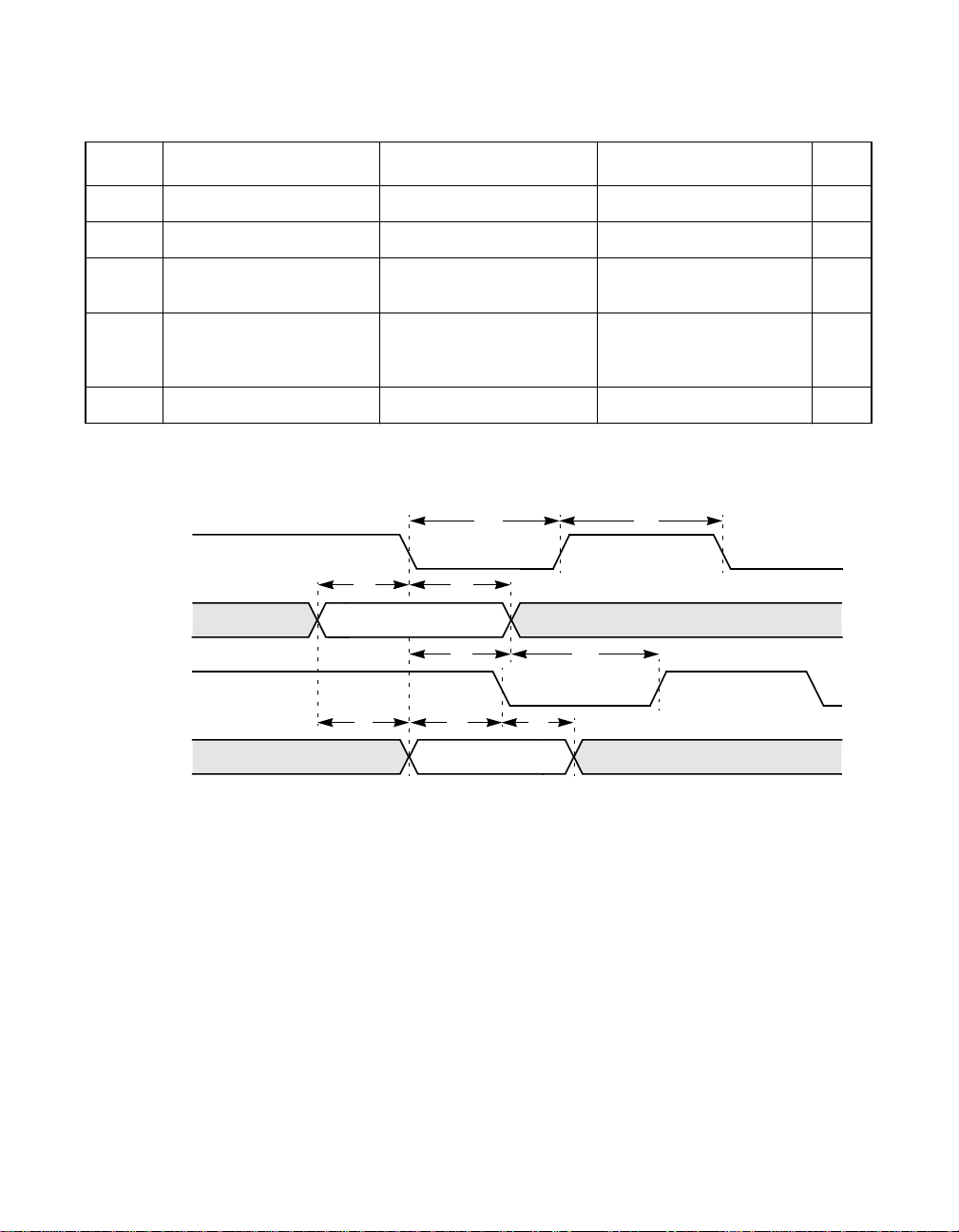
Table 3.18 Output Timing
Symbol Parameter Min Max Units
t
Output data setup Nominal: negotiated/2 – ns
5
t
Output data hold Nominal: negotiated/2 – ns
6
t
Output REQ/ACK pulse
7
width
t
REQ/ACK transport delay 25 ns if REQ/ACK is clock
8
t
Data transport delay 6 [t3+ 35] ns
9
max [negotiated ns, t3− 5] max [negotiated ns, t3+5] ns
for input data,
10 ns if not
50 ns if REQ/ACK is clock
for input data,
30 ns if not
ns
Figure 3.13 Input/Output Timing
Input Timing
REQ or ACK
Data
Output Timing
REQ or ACK
Data
t
1
Valid Data
t
9
t
3
t
2
t
8
t
5
Valid Data
t
4
t
7
t
6
3-22 LSI53C140 Specifications
Ver. 2.1 Copyright © 1998–2001 by LSI Logic Corporation. All rights reserved.
Page 57

3.3 Mechanical Drawings
LSI Logic component dimensions conform to a current revision of the
JEDEC Publication 95 standard package outline, using ANSI 14.5Y
“Dimensioning and Tolerancing” interpretations. As JEDEC drawings are
balloted and updated, changes may have occurred. To ensure the use of
a current drawing, the JEDEC drawing revision level should be verified.
Visit www.eia.org/jedec for review of Publication 95 drawings and
revision levels.
For printed circuit board land patterns that will accept LSI Logic
components, LSI Logic recommends that customers refer to the IPC
standards (Institute for Interconnecting and Packaging Electronic
Circuits). Specification number IPC-SM-782, “Surface Mount Design and
Land Pattern Standard” is an established method of designing land
patterns. Feature size and tolerances are industry standards based on
IPC assumptions.
Mechanical Drawings 3-23
Ver. 2.1 Copyright © 1998–2001 by LSI Logic Corporation. All rights reserved.
Page 58

3.3.1 LSI53C140 160-Pin PQFP Mechanical Drawing
The LSI53C140 is packaged in a 160-pin metric PQFP. Figure 3.14 is the
package drawing for the LSI53C140.
Figure 3.14 LSI53C140 160-Pin PQFP (PF) Mechanical Drawing
Important: This drawing may not be the latest version. For board layout and manufacturing, obtain the
most recent engineering drawings from your LSI Logic marketing representative by
requesting the outline drawing for package code PF.
3-24 LSI53C140 Specifications
Ver. 2.1 Copyright © 1998–2001 by LSI Logic Corporation. All rights reserved.
Page 59

Figure 3.14 LSI53C140 160-Pin PQFP (PF) Mechanical Drawing (Cont.)
Important: This drawing may not be the latest version. For board layout and manufacturing, obtain the
most recent engineering drawings from your LSI Logic marketing representative by
requesting the outline drawing for package code PF.
Mechanical Drawings 3-25
Ver. 2.1 Copyright © 1998–2001 by LSI Logic Corporation. All rights reserved.
Page 60

3.3.2 LSI53C140 192-Ball PBGA Mechanical Drawing
The LSI53C140 is available as a 192-ball PBGA. Figure 3.15 illustrates
the 192-ball PBGA mechanical drawing. Refer to Appendix B for more
detailed information.
Figure 3.15 192-Ball PBGA (IJ, I2) Mechanical Drawing
Important: This drawing may not be the latest version. For board layout and manufacturing, obtain the
most recent engineering drawings from your LSI Logic marketing representative by
requesting the outline drawing for package code IJ, I2.
3-26 LSI53C140 Specifications
Ver. 2.1 Copyright © 1998–2001 by LSI Logic Corporation. All rights reserved.
Page 61

Appendix A
Wiring Diagrams
Figure A.1 illustrates a typical LSI53C140 in an evaluation test board
application. Figure A.2 shows the wiring diagram for Ultra SCSI operation
in the differential mode using pull-up resistors.
LSI53C140 Ultra2 SCSI Bus Expander A-1
Ver. 2.1 Copyright © 1998–2001 by LSI Logic Corporation. All rights reserved.
Page 62

Figure A.1 LSI53C140 Wiring Diagram 1 of 4
A-2 Wiring Diagrams
Ver. 2.1 Copyright © 1998–2001 by LSI Logic Corporation. All rights reserved.
Page 63

Figure A.1 LSI53C140 Wiring Diagram 2 of 4
A-3
Ver. 2.1 Copyright © 1998–2001 by LSI Logic Corporation. All rights reserved.
Page 64

Figure A.1 LSI53C140 Wiring Diagram 3 of 4
A-4 Wiring Diagrams
Ver. 2.1 Copyright © 1998–2001 by LSI Logic Corporation. All rights reserved.
Page 65

Ver. 2.1 Copyright © 1998–2001 by LSI Logic Corporation. All rights reserved.
Figure A.1 LSI53C140 Wiring Diagram 4 of 4
Connector Page
A-5
Test circuit switch only.
Test circuit switch only.
Page 66

Figure A.2 LSI53C140 Differential Wiring Diagram
LSI53C140
MSG−
SD[8:15]+
SDP1+
SD[8:15]−
SDP1−
SDP0+
SDP0−
DIFFSENS
SEL+
BSY+
RST+
SEL−
BSY−
RST−
REQ−
ACK−
C/D−
I/O−
ATN−
REQ+
ACK+
SD7+
SD6+
SD5+
SD4+
SD3+
SD2+
SD1+
SD0+
SD7−
SD6−
SD5−
SD4−
SD3−
SD2−
SD1−
SD0−
Float
Float
VDD
1.5 K
VDD
DIFFSENS
1.5 K
VDD
VDD
1.5 K
1.5 K
1.5 K
VDD
1.5 K
1.5 K
1.5 K
1.5 K
SELBSYRST-
1.5 K
SD0−
SD1−
SD2−
SD3−
SD4−
SD5−
SD6−
SD7−
SDP0−
VDD
1.5 K
SEL+
BSY+
RST+
REQ/
ACK−
MSG−
C_D−
I_O−
ATN-
DIFFSENS
SD0+
SD1+
SD2+
SD3+
SD4+
SD5+
SD6+
SD7+
SDP0+
DIFFSENS
Schottky
Diode
SN75976A2
CDE0
CDE1
CDE2
BSR
CRE
1A
1DE/RE
2A
2DE/RE
3A
3DE/RE
4A
4DE/RE
5A
5DE/RE
6A
6DE/RE
7A
7DE/RE
8A
8DE/RE
9A
9DE/RE
SN75976A2
CDE0
CDE1
CDE2
BSR
CRE
1A
1DE/RE
2A
2DE/RE
3A
3DE/RE
4A
4DE/RE
5A
5DE/RE
6A
6DE/RE
7A
7DE/RE
8A
8DE/RE
9A
9DE/RE
DIFFSENS (pin 21)
−SEL
+SEL
−BSY
+BSY
−RST
+RST
−REQ
+REQ
−ACK
+ACK
−MSG
+MSG
−C/D
+C/D
−I/O
+I/O
−ATN
+ATN
−DB0
+DB0
−DB1
+DB1
−DB2
+DB2
−DB3
+DB3
−DB4
+DB4
−DB5
+DB5
−DB6
+DB6
−DB7
+DB7
−DBP
+DBP
(42)
(41)
(34)
(33)
(38)
(37)
(46)
(45)
(36)
(35)
(40)
(39)
(44)
(43)
(48)
(47)
(30)
(29)
(4)
(3)
(6)
(5)
(8)
(7)
(10)
(9)
(12)
(11)
(14)
(13)
(16)
(15)
(18)
(17)
(20)
(19)
1B+
1B−
2B+
2B−
3B+
3B−
4B+
4B−
5B+
5B−
6B+
6B−
7B+
7B−
8B+
8B−
9B+
9B−
1B+
1B−
2B+
2B−
3B+
3B−
4B+
4B−
5B+
5B−
6B+
6B−
7B+
7B−
8B+
8B−
9B+
9B−
SCSI
Bus
A-6 Wiring Diagrams
Ver. 2.1 Copyright © 1998–2001 by LSI Logic Corporation. All rights reserved.
Page 67

Appendix B
Board Design
Considerations
This appenidx describes the design considerations for using the
LSI53C180 as a drop in replacement for the LSI53C140. Both chips are
available as a 192-ball PBGA in a 23 x 23 mm package. This appendix
also describes the differences in pin configurations required for operation
of the two devices.
The LSI53C180 supports Ultra160 data transfer rates for an LVD bus and
Ultra data transfer rates for an SE bus. The LSI53C180 does not support
HVD. Thus, HVD mode enable pins for each port are no longer present.
In the LSI53C140, pins B7 and A3 should be pulled to GND to disable
HVD mode when operating in SE or LVD mode. These two pins are no
connects in the LSI53C180.
The LSI53C180 has an independent RBIAS pin to control margining for
each bus, rather than a single pin for both buses as implemented in the
LSI53C140. A 10 kΩ pull-up resistor on RBIAS is recommended to
provide the correct margining. If initially designing for the LSI53C140 with
the intention of upgrading to the LSI53C180 at a later time, a footprint
from the pull-up resistor for the A-RBIAS signal should be implemented.
Table B.1 summarizes the information in the previous paragraphs.
Table B.1 Pin Adjustments
Pin
Number LSI53C140 Signal LSI53C180 Signal
K17 NC A-RBIAS
B7 A_HVD_MODE NC
A3 B_HVD_MODE NC
LSI53C140 Ultra2 SCSI Bus Expander B-1
Ver. 2.1 Copyright © 1998–2001 by LSI Logic Corporation. All rights reserved.
Page 68

Table B.2 lists all of the no connect pins for the LSI53C140 and
LSI53C180.
Table B.2 No Connect Pins
Signal No Connect (NC) Pins
LSI53C140 D3, F3, L2, T1, U1, R4, U6, R10, R12, U16, U17, P15, H15,
LSI53C180 D3, F3, L2, T1, U1, R4, U6, R10, R12, U16, U17, P15, H15,
F15, C15, C14, A17, A5, C6, B4, A4, C4, B3
F15, C15, C14, A17, A5, C6, B4, A4, C4, B3, A3, B7
B-2 Board Design Considerations
Ver. 2.1 Copyright © 1998–2001 by LSI Logic Corporation. All rights reserved.
Page 69

Appendix C
Glossary
ACK/ Acknowledge – Driven by an initiator,ACK/ indicates an acknowledgment
or a SCSI data transfer. In the target mode, ACK/ is received as a
response to the REQ/ Signal.
ANSI American National Standards Institute.
Arbitration The process of selecting one respondent from a collection of several
candidates that request service concurrently.
Asserted A signal is asserted when it is in the state that is indicated by the name of
the signal. Opposite of negated or deasserted.
Assertion The act of driving a signal to the true state.
Asynchronous
Transmission
ATN/ Attention – Driven by an initiator, indicates an attention condition. In the
Block A block is the basic 512 byte size of storage that the storage media is
BSY/ Busy – Indicates that the SCSI Bus is being used. BSY/ can be driven by
Bus Acollection of unbroken signal lines that interconnect computer modules.
Bus Expander Bus expander technology permits the extension of a bus by providing
Transmission in which each byte of the information is synchronized
individually through the use of Request (REQ/) and Acknowledge (ACK/)
signals.
target role, ATN/ is received and is responded to by entering the Message
Out Phase.
divided into. The Logical Block Address protocol uses sequential block
addresses to access the media.
the initiator or the target device.
The connections are made by taps on the lines.
some signal filtering and retiming to maintain signal skew budgets.
LSI53C140 Ultra2 SCSI Bus Expander C-1
Ver. 2.1 Copyright © 1998–2001 by LSI Logic Corporation. All rights reserved.
Page 70

Cable Skew
Delay
Cable skew delay is the minimum difference in propagation time allowed
between any two SCSI bus signals measured between any two SCSI
devices.
C_D/ Control/Data – Driven by a target. When asserted, indicates Control or
Data Information is on the SCSI Bus. This signal is received by the
initiator.
Connect The function that occurs when an initiator selects a target to start an
operation, or a target reselects an initiator to continue an operation.
Control Signals The set of nine lines used to put the SCSI bus into its different phases.
The combinations of asserted and negated control signals define the
phases.
Controller A computer module that interprets signals between a host and a
peripheral device. Often, the controller is a part of the peripheral device,
such as circuitry on a disk drive.
DB[7:0]/ SCSI Data Bits – These eight Data Bits (DB[7:0]/), plus a Parity Bit
(DBP/), form the SCSI Bus. DB7/ is the most significant bit and has the
highest priority ID during the Arbitration Phase. Data parity is odd. Parity
is always generated and optionally checked. Parity is not valid during
arbitration.
Deasserted The act of driving a signal to the false state or allowing the cable
terminators to bias the signal to the false state (by placing the driver in the
high impedance condition).
A signal is deasserted or negated when it is in the state opposite to that
which is indicated by the name of the signal. Opposite of asserted.
Device A single unit on the SCSI bus, identifiable by a SCSI address. It can be a
processor unit, a storage unit (such as a disk or tape controller or drive),
an output unit (such as a controller or printer), or a communications unit.
Differential A signaling alternative that employs differential drivers and receivers to
improve signal-to-noise ratios and increase maximum cable lengths.
Disconnect The function that occurs when a target releases control of the SCSI bus,
allowing the bus to go to the Bus Free phase.
Driver When used in the context of electrical configuration, “driver” is the
circuitry that creates a signal on a line.
C-2 Glossary
Ver. 2.1 Copyright © 1998–2001 by LSI Logic Corporation. All rights reserved.
Page 71

External
Configuration
All SCSI peripheral devices are external to the host enclosure.
External
Terminator
The terminator that exists on the last peripheral device that terminates the
end of the external SCSI bus.
Free In the context of Bus Free phase, “free” means that no SCSI device is
actively using the SCSI bus and, therefore, the bus is available for use.
Host A processor, usually consisting of the central processing unit and main
memory. Typically, a host communicates with other devices, such as
peripherals and other hosts. On the SCSI bus, a host has a SCSI
address.
Host Adapter Circuitry that translates between a processor's internal bus and a different
bus, such as SCSI. On the SCSI bus, a host adapter usually acts as an
initiator.
Initiator A SCSI device that requests another SCSI device (a target) to perform an
operation. Usually, a host acts as an initiator and a peripheral device acts
as a target.
Internal
All SCSI peripheral devices are internal to the host enclosure.
Configuration
Internal
Terminator
The terminator that exists within the host that terminates the internal end
of the SCSI bus.
I/O Input/Output – Driven by a target. I/O controls the direction of data
transfer on the SCSI Bus. When active, this signal indicates input to the
initiator. When inactive, this signal indicates output from the initiator. This
signal is also used to distinguish between the Selection and Reselection
Phases.
I/O Cycle An I/O cycle is an Input (I/O Read) operation or Output (I/O Write)
operation that accesses the PC Card’s I/O address space.
Logical Unit The logical representation of a physical or virtual device, addressable
through a target. A physical device can have more than one logical unit.
Low (logical
A signal is at the low logic level when it is below approximately 0.5 volts.
level)
Glossary C-3
Ver. 2.1 Copyright © 1998–2001 by LSI Logic Corporation. All rights reserved.
Page 72

LSB Abbreviation for Least Significant Bit or Least Significant Byte. That
portion of a number, address or field that occurs right-most when its value
is written as a single number in conventional hexadecimal or binary
notation. The portion of the number having the least weight in a
mathematical calculation using the value.
LUN Logical Unit Number. Used to identify a logical unit.
Mandatory A characteristic or feature that must be present in every implementation of
the standard.
MHz MegaHertz – Measurement in millions of Hertz per second. Used as a
measurement of data transfer rate.
microsecond
One millionth of a second.
(µs)
MSB Abbreviation for Most Significant Bit or Most Significant Byte. That portion
of a number, address or field that occurs left-most when its value is
written as a single number in conventional hexadecimal or binary
notation. The portion of the number having the most weight in a
mathematical calculation using the value.
MSG/ Message – Driven active by a target during the Message Phase. This
signal is received by the initiator.
nanosecond
One billionth of a second.
(ns)
Negated A signal is negated or deasserted when it is in the state opposite to that
which is indicated by the name of the signal. Opposite of asserted.
Negation The act of driving a signal to the false state or allowing the cable
terminators to bias the signal to the false state.
Parity A method of checkingthe accuracy of binary numbers. An extrabit, called
a parity bit, is added to a number. If even parity is used, the sum of all 1s
in the number and its corresponding parity is always even. If odd parity is
used, the sum of the 1s and the parity bit is always odd.
Peripheral
device
A device that can be attached to the SCSI bus.Typical peripheral devices
are disk drives, tape drives, printers, CD ROMs, or communications units.
Phase One of the eight states to which the SCSI bus can be set. During each
phase, different communication tasks can be performed.
Port A connection into a bus.
C-4 Glossary
Ver. 2.1 Copyright © 1998–2001 by LSI Logic Corporation. All rights reserved.
Page 73

Priority The ranking of the devices on the bus during arbitration.
Protocol A convention for data transmission that encompasses timing control,
formatting, and data representation.
Receiver The circuitry that receives electrical signals on a line.
Reconnect The function that occurs when a target reselects an initiator to continue an
operation after a disconnect.
Release The act of allowing the cable terminators to bias the signal to the false
state (by placing the driver in the high impedance condition).
REQ/ Request – Driven by a target, indicates a request for a SCSI data-transfer
handshake. This signal is received by the initiator.
Reselect A target can disconnect from an initiator in order to perform a time-
consuming function, such as a disk seek. After performing the operation,
the target can “reselect” the initiator.
RESET Reset – Clears all internal registers when active. It does not assert the
SCSI RST/ signal and therefore does not reset the SCSI bus.
RST Reset – Indicates a SCSI Bus reset condition.
SCSI Small Computer System Interface.
SCSI Address The octal representation of the unique address ([7:0]) assigned to a SCSI
device. This address is normally assigned and set in the SCSI device
during system installation.
SCSI ID
Identification)
The bit-significant representation of the SCSI address referring to one of
the signal lines DB7/ through DB0/.
or SCSI Device
ID
SCAM An acronym for SCSI Configured AutoMatically. SCAM is the new SCSI
automatic ID assignment protocol. SCAM frees SCSI users from locating
and setting SCSI ID switches and jumpers. SCAM is the key part of Plug
and Play SCSI.
SDTR Synchronous Data Transfer Request messages are used to negotiate a
synchronous data transfer agreement between two SCSI devices. An
SDTR agreement applies to all logical units of the two SCSI devices that
negotiated agreement.
SEL/ Select – Used by an initiator to select a target, or by a target to reselect an
initiator.
Glossary C-5
Ver. 2.1 Copyright © 1998–2001 by LSI Logic Corporation. All rights reserved.
Page 74

Single-Ended
Configuration
An electrical signal configuration that uses a single line for each signal,
referenced to a ground path common to the other signal lines. The
advantage of a single-ended configuration is that it uses half the pins,
chips, and board area that differential/low-voltage differential
configurations require. The main disadvantage of single-ended
configurations is that they are vulnerable to common mode noise. Also,
cable lengths are limited.
Synchronous
Transmission
Transmission in which the sending and receiving devices operate
continuously at the same frequency and are held in a desired phase
relationship by correction devices. For buses, synchronous transmission
is a timing protocol that uses a master clock and has a clock period.
Target A SCSI device that performs an operation requested by an initiator.
Termination The electrical connection at each end of the SCSI bus, composed of a set
of resistors.
µs Microsecond. One millionth of a second.
WDTR Wide Data Transfer Request messages are used to negotiate a wide data
transfer agreement between two SCSI devices. A WDTR agreement
applies to all logical units of the two SCSI devices that negotiated the
agreement.
C-6 Glossary
Ver. 2.1 Copyright © 1998–2001 by LSI Logic Corporation. All rights reserved.
Page 75

Index
Numerics
160-pin plastic quad flat pack 1-7
160-pin PQFP 3-24
pin diagram 3-3
192-ball PBGA 3-26
ball diagram 3-4
192-ball plastic ball grid array 1-7
3-state 2-8
leakage 3-14
A
A_DIFFSENS 3-7
A_HVD_MODE 3-7
A_SACK 2-10
A_SACK+/- 3-7
A_SATN 2-11
A_SATN+/- 3-7
A_SBSY 2-9
A_SBSY+/- 3-7
A_SCD 2-11
A_SCD+/- 3-7
A_SD[15:0] 2-7
A_SD[15:0]+/- 3-7
A_SDP[1:0] 2-7
A_SDP[1:0]+/- 3-7
A_SIO 2-11
A_SIO+/- 3-7
A_SMSG 2-11
A_SMSG+/- 3-7
A_SREQ 2-10
A_SREQ+/- 3-7
A_SRST 2-9
A_SRST+/- 3-7
A_SSEL 2-8
A_SSEL+/- 3-7
absolute maximum stress ratings 3-11
AC characteristics 3-21
acknowledge 2-3
(SACK) 2-10
active negation 2-3
applications 1-3
attention (SATN) 2-11
B
B_DIFFSENS 3-8
B_HVD_MODE 3-8
B_SACK 2-10
B_SACK+/- 3-8
B_SATN 2-11
B_SATN+/- 3-8
B_SBSY 2-9
B_SBSY+/- 3-8
B_SCD 2-11
B_SCD+/- 3-8
B_SD[15:0] 2-7
B_SD[15:0]+/- 3-8
B_SDP[1:0] 2-7
B_SDP[1:0]+/- 3-8
B_SIO 2-11
B_SIO+/- 3-8
B_SMSG 2-11
B_SMSG+/- 3-8
B_SREQ 2-10
B_SREQ+/- 3-8
B_SRST 2-9
B_SRST+/- 3-8
B_SSEL 2-8
B_SSEL+/- 3-8
backward compatibility 1-8
balanced duty cycles 2-3
bidirectional
connections 2-2
SCSI Signals 3-15
SCSI signals 3-14
BSY_LED 2-8, 3-9
bus timing 2-5
busy (BSY) 2-9
C
calibration 2-5
chip reset (RESET/) 2-13
CLOCK 3-9
clock
(CLOCK) 2-15
signal 2-8
timing 3-21
control/data (SCD) 2-11
D
data 2-3, 2-7
DC characteristics 3-11
delay settings 2-5
differential transceivers 1-8
DIFFSENS 2-4, 2-5
receiver 2-5
DIFFSENS SCSI Signals 3-14
direction control signal polarities 2-12
double clocking of data 2-3
LSI53C140 Ultra2 SCSI Bus Expander IX-1
Ver. 2.1 Copyright © 1998–2001 by LSI Logic Corporation. All rights reserved.
Page 76

E
electrical characteristics 3-11
electrostatic discharge 3-11
enable/disable SCSI transfers 3-9
ESD 3-11
F
filter edges 2-10
G
glitches 2-3
H
high voltage differential SCSI 1-7
HVD_MODE control signal polarity 2-12
hysteresis 2-7
hysteresis of SCSI receivers 3-19
I
input
capacitance 3-14
I/O pads 3-14
input pads 3-14
control signals 3-15
high voltage 3-14
low voltage 3-14
timing 3-21
voltage 3-11
voltage (TolerANT pins) 3-11
input current as a function of input voltage 3-20
input/output (SIO) 2-11
interface control pins 3-9
L
latch-up current 3-11
leading edge filter 2-8, 2-10
load bus 2-7
LSI53C140 SCSI bus expander 1-1
LVD
DIFFSENS 2-5
driver SCSI signals 3-12
receiver SCSI signals 3-13
LVDlink 1-8
benefits 1-7, 1-8
technology 2-4
transceivers 1-8, 2-4
M
master reset 3-9
mechanical drawings 3-23
message (SMSG) 2-11
migration path 1-8
O
operating conditions 3-12
operating free air 3-12
output
control signals 3-16
high voltage 3-14
low voltage 3-14
timing 3-22
output current as a function of output voltage 3-20
P
parallel function 2-9, 2-10
parity 2-3, 2-7
PBGA 1-7
pin adjustments
board design B-1
pins
no connect B-2
power
on reset (POR) 2-13
PQFP 1-7
precision
delay control 2-1, 2-4
pull-down 2-8, 2-11
pull-up 2-8, 2-11
pulse width 2-10
R
RBIAS 3-10
RC-type input filters 2-3
receiver latch 2-8
recovery 2-11
reliability issue 2-3
request 2-3
(SREQ) 2-10
reset (SRST) 2-9
RESET/ 2-13, 3-9
control signal polarity 2-13
retiming 2-10
logic 2-1, 2-5
rise and fall time test conditions 3-19
S
SACK 2-10
SCSI
bus protocol 2-5
I/O logic 2-11
parallel Interface-2 1-7
phases 2-4
signal descriptions 3-7
TolerANT technology 2-3
SCSI bus free state 2-14
SCSI enhanced parallel interface 1-7
SCSI input filtering 3-19
SCSI interface timing 3-21
select (SSEL) 2-8
server clustering 1-3
signal
descriptions 3-2
groupings 2-6
skew 2-2
IX-2 Index
Ver. 2.1 Copyright © 1998–2001 by LSI Logic Corporation. All rights reserved.
Page 77

source bus 2-2, 2-7
SREQ 2-10
SSEL 2-8
state machine 2-10
control 2-1, 2-4, 2-5
storage temperature 3-11
supply voltage 3-11
T
temperature 2-5
thermal resistance
BGA package 3-12
QFP package 3-12
TolerANT
drivers and receivers 2-3
receiver technology 2-3
SCSI 2-3
technology 2-3
benefits 2-3
TolerANT technology electrical characteristics 3-17
V
VDD_CORE 3-10
VDD_IO 3-10
VDD_SCSI 3-10
voltage 2-5
VSS 3-10
W
warm swap enable 2-14
wide Ultra2 SCSI 2-2
wiring diagram
evaluation test board A-2
Ultra SCSI differential mode A-6
WS_ENABLE 2-14, 3-9
signal polarity 2-14
X
XFER_ACTIVE 2-14, 3-9
signal polarity 2-14
Index IX-3
Ver. 2.1 Copyright © 1998–2001 by LSI Logic Corporation. All rights reserved.
Page 78

IX-4 Index
Ver. 2.1 Copyright © 1998–2001 by LSI Logic Corporation. All rights reserved.
Page 79

Customer Feedback
We would appreciate your feedback on this document. Please copy the
following page, add your comments, and fax it to us at the number
shown.
If appropriate, please also fax copies of any marked-up pages from this
document.
Important: Please include your name, phone number, fax number, and
company address so that we may contact you directly for
clarification or additional information.
Thank you for your help in improving the quality of our documents.
LSI53C140 Ultra2 SCSI Bus Expander
Ver. 2.1 Copyright © 1998–2001 by LSI Logic Corporation. All rights reserved.
Page 80

Reader’s Comments
Fax your comments to: LSI Logic Corporation
Technical Publications
M/S E-198
Fax: 408.433.4333
Please tell us how you rate this document: LSI53C140 Ultra2 SCSI Bus
Expander. Place a check mark in the appropriate blank for each category.
Excellent Good Average Fair Poor
Completeness of information ____ ____ ____ ____ ____
Clarity of information ____ ____ ____ ____ ____
Ease of finding information ____ ____ ____ ____ ____
Technical content ____ ____ ____ ____ ____
Usefulness of examples and
illustrations
Overall manual ____ ____ ____ ____ ____
____ ____ ____ ____ ____
What could we do to improve this document?
If you found errors in this document, please specify the error and page
number. If appropriate, please fax a marked-up copy of the page(s).
Please complete the information below so that we may contact you
directly for clarification or additional information.
Name
Telephone
Fax
Date
Title
Department Mail Stop
Company Name
Street
City, State, Zip
Customer Feedback
Ver. 2.1 Copyright © 1998–2001 by LSI Logic Corporation. All rights reserved.
Page 81

You can find a current list of our U.S. distributors, international distributors, and sales
offices and design resource centers on our web site at
http://www.lsilogic.com/contacts/na_salesoffices.html
Page 82

 Loading...