

Page 1

TECHNICAL
MANUAL
LSI53C120
Ultra SCSI Bus Expander
August 2001
Version 1.0
®
DB14-000181-00
Page 2

This document contains proprietary information of LSI Logic Corporation. The
information contained herein is not to be used by or disclosed to third parties
without the express written permission of an officer of LSI Logic Corporation.
LSI Logic products are not intended for use in life-support appliances, devices,
or systems. Use of any LSI Logic product in such applications without written
consent of the appropriate LSI Logic officer is prohibited.
Document DB14-000181-00, First Edition (August 2001)
This document describes LSI Logic Corporation’s LSI53C120 Ultra SCSI Bus
Expander and will remain the official reference source for all revisions/releases
of this product until rescinded by an update.
LSI Logic Corporation reserves the right to make changes to any products herein
at any time without notice. LSI Logic does not assume any responsibility or
liability arising out of the application or use of any product described herein,
except as expressly agreed to in writing by LSI Logic; nor does the purchase or
use of a product from LSI Logic convey a license under any patent rights,
copyrights, trademark rights, or any other of the intellectual property rights of LSI
Logic or third parties.
Copyright © 1996-2001 by LSI Logic Corporation. All rights reserved.
TRADEMARK ACKNOWLEDGMENT
The LSI Logic logo design and TolerANT are trademarks or registered
trademarks of LSI Logic Corporation. All other brand and product names may be
trademarks of their respective companies.
MH
To receive product literature, visit us at http://www.lsilogic.com.
For a current list of our distributors, sales offices, and design resource
centers, view our web page located at
http://www.lsilogic.com/contacts/na_salesoffices.html
ii
Page 3

Audience
Preface
This book is the primary reference and technical manual for the
LSI53C120 Ultra SCSI Bus Expander. It contains a complete functional
description and complete physical and electrical specifications for the
LSI53C120 Ultra SCSI Bus Expander chip, which supports single-ended
to single-end SCSI bus expansion (Extender) or single-ended to
differential SCSI bus conversion (Converter).
This manual assumes some prior knowledge of current and proposed
SCSI standards. For background information, please contact:
ANSI
11 West 42nd Street
New York, NY 10036
(212) 642-4900
Ask for document number X3.131-1994 (SCSI-2) (SCSI-3)
Global Engineering Documents
15 Inverness Way East
Englewood, CO 80112
(800) 854-7179 or (303) 792-2181 (outside U.S.)
Ask for document number X3.131-1994 (SCSI-2) or X3.253 (SCSI-3
Parallel Interface)
ENDL Publications
14426 Black Walnut Court
Saratoga, CA 95070
(408) 867-6642
Document names: SCSI Bench Reference, SCSI Encyclopedia
Prentice Hall
Englewood Cliffs, NJ 07632
Preface iii
Page 4

(201) 767-5937
Ask for document number ISBN 0-13-796855-8, SCSI: Understanding
the Small Computer System Interface
LSI Logic World Wide Web
http://www.lsilogic.com
(See EPI (Enhanced Parallel Interface) Specification for expander
configurations)
Revision Record
Revision Date Remarks
1.0 8/01 All product name changes from a SYM to an LSI prefix. Updated
Organization
This document has the following chapters and appendixes:
figure references throughout book. Updated wiring diagram in
Appendix A.
• Chapter 1, Introduction, provides general information about the
LSI53C120 Ultra SCSI Bus Expander.
• Chapter 2, Functional Description, provides information about the
interface signal descriptions.
• Chapter 3, Specifications, describes the LSI53C120 as a 128-pin
PQFP. It also provides minimum and maximum values for the
electrical characteristics of this expander/converter.
• Appendix A, Differential Wiring Diagram, illustrates the LSI53C120
wiring diagram for Ultra SCSI operation.
• Appendix B, Glossary, provides definitions for key terms used in this
manual.
Related Publication
LSI53C141 SCSI Bus Expander, Version 2.1, LSI Logic Corporation,
Order No. S14013.A
iv Preface
Page 5

Conventions Used in This Manual
The word assert means to drive a signal true or active. The word
deassert means to drive a signal false or inactive. Signals that are active
LOW end in a slash mark (/).
Preface v
Page 6

vi Preface
Page 7

Contents
Chapter 1 Introduction
1.1 General Description 1-1
1.2 Features 1-3
1.3 Application Examples 1-4
1.3.1 Scalable Device Connectivity 1-4
1.3.2 SCSI Bus Electrical Isolation 1-6
Chapter 2 Functional Description
2.1 Interface Signal Descriptions 2-1
2.1.1 SCSI A-Side and B-Side Single-Ended
Control Blocks 2-2
2.1.2 Re-timing Logic 2-3
2.1.3 Precision Delay Control 2-3
2.1.4 State Machine Control 2-4
2.1.5 Differential Control 2-4
2.2 SCSI Signal Descriptions 2-4
2.2.1 Data and Parity 2-5
2.2.2 Busy (BSY) Control 2-6
2.2.3 Reset (RST) Control 2-7
2.2.4 Request (REQ)/Acknowledge (ACK) Control 2-7
2.2.5 Control/Data (C/D), Input/Output (I/O),
Message (MSG) and Attention (ATN) Controls 2-8
2.2.6 Differential Direction Controls 2-8
2.2.7 Differential Mode (DIFF_MODE/) 2-9
2.2.8 Differential Sense (DIFF_SENSE) 2-9
2.2.9 Control Signals 2-10
Contents vii
Page 8

Chapter 3 Specifications
3.1 Signal Descriptions 3-1
3.1.1 LSI53C120 Pin Diagram 3-1
3.1.2 LSI53C120 Signal Grouping 3-3
3.1.3 SCSI A Interface Pins 3-4
3.1.4 SCSI B Single-ended Interface Pins 3-5
3.1.5 SCSI B Differential Interface Pins 3-6
3.1.6 Control Interface Pins 3-7
3.2 Electrical Characteristics 3-8
3.2.1 DC Characteristics 3-8
3.2.2 TolerANT Technology Electrical Characteristics 3-12
3.2.3 AC Characteristics 3-15
3.3 LSI53C120 Mechanical Drawing 3-17
Appendix A Differential Wiring Diagram
Appendix B Glossary
Index
Customer Feedback
viii Contents
Page 9

Figures
1.1 LSI53C120 SCSI Bus Device 1-2
1.2 SCSI Extender Application (SE to SE Mode of Operation) 1-5
1.3 SCSI Extender or Converter Application (SE to HVD Mode
of Operation) 1-5
1.4 SCSI Bus Electrical Isolation 1-6
2.1 LSI53C120 Block Diagram 2-2
2.2 LSI53C120 Signal Grouping 2-5
3.1 LSI53C120 Pin Diagram 3-2
3.2 LSI53C120 Functional Signal Grouping 3-3
3.3 Rise and Fall Time Test Conditions 3-13
3.4 SCSI Input Filtering 3-13
3.5 Hysteresis of SCSI Receiver 3-14
3.6 Input Current as a Function of Input Voltage 3-14
3.7 Output Current as a Function of Output Voltage 3-15
3.8 Clock Timing 3-16
3.9 Input/Output Timing 3-17
3.10 LSI53C120 Mechanical Drawing 3-18
A.1 LSI53C120 Differential Wiring Diagram A-2
ix
Page 10

x
Page 11

Tables
1.1 Modes of Operation 1-1
2.1 Direction Control Signals (B_SDIR(15-0, P0, P1), B_BSYDIR,
B_SELDIR, B_CD_DIR, B_IO_DIR, B_MSGDIR, B_REQDIR,
B_ACKDIR, B_ATNDIR and B_RSTDIR) Polarities 2-9
2.2 DIFF_MODE/ Control Signal Polarity 2-9
2.3 DIFF_SENSE Control Signal Polarity 2-10
2.4 RESET/ Control Signal Polarity 2-10
2.5 WS_ENABLE/ Signal Polarity 2-11
2.6 XFER_ACTIVE Signal Polarity 2-11
3.1 SCSI A Signal Description 3-4
3.2 SCSI B Signal Description 3-5
3.3 SCSI B Differential Signal Description 3-6
3.4 Chip Control Signal Description 3-7
3.5 SCSI Control Signal Description 3-7
3.6 Power and Ground Signal Description 3-7
3.7 No Connect Pins 3-8
3.8 Absolute Maximum Stress Ratings 3-8
3.9 Operating Conditions 3-9
3.10 SCSI Signals – A_SD(15-0)/, A_SDP(1-0)/, A_SREQ/,
A_SACK/, B_SD(15-0)/, B_SDP(1-0)/, B_SREQ/, B_SACK/ 3-9
3.11 SCSI Signals – A_SMSG, A_SI_O/, A_SC_D/, A_SATN/,
A_SBSY/, A_SSEL/, A_SRST/, B_SMSG, B_SI_O/,
B_SC_D/, B_SATN/, B_SBSY/, B_SSEL/, B_SRST/ 3-10
3.12 Input Signals – CLOCK, DIFF_SENSE, DIFF_MODE/*,
WS_ENABLE/* 3-10
3.13 Capacitance 3-10
3.14 Differential Signals - B_SDIR(15-0), B_SDIRP0, B_SDIRP1,
B_CD_DIR, B_IO_DIR, B_MSGDIR, B_REQDIR,
B_B_ACKDIR, B_BSYDIR, B_SELDIR, B_RSTDIR 3-11
3.15 Control Signals - RESET/ 3-11
3.16 Control Signals - XFER_ACTIVE 3-11
3.17 TolerANT Technology Electrical Characteristics 3-12
3.18 Clock Timing 3-15
3.19 Input Timing 3-16
3.20 Output Timing 3-16
xi
Page 12

xii
Page 13

Chapter 1
Introduction
This chapter describes the LSI53C120 Ultra SCSI Bus Expander and its
applications. It includes these topics:
• Section 1.1, “General Description,” page 1-1
• Section 1.2, “Features,” page 1-3
• Section 1.3, “Application Examples,” page 1-4
1.1 General Description
The LSI53C120 Ultra SCSI Bus Expander is a single chip solution
allowing the extension of device connectivity and/or cable length limits of
the SCSI bus. The LSI53C120 operates as a Ultra SCSI bus expander
when multiple single-ended to single-ended cables are connected
together while being electrically isolated from each other.TheLSI53C120
also operates as a SCSI bus converter when single-ended to differential
cables are connected together while being electrically isolated from each
other.
The LSI53C120 operates in two modes: single-ended to single-ended
(Extender Mode) or single-ended to High Voltage Differential (HVD)
(Converter Mode). For applications requiring SE to Low Voltage
Differential (LVD), use the LSI53C141 SCSI Bus Expander. Table 1.1
shows all modes of operation.
Table 1.1 Modes of Operation
Product Extender Converter
LSI53C120 SE to SE SE to HVD
LSI5353C141 SE to SE SE to LVD
LSI53C120 Ultra SCSI Bus Expander 1-1
Page 14
In both SCSI Bus Extender and Converter modes, cable segments are
electrically isolated from each other. This feature maintains the signal
integrity of each cable segment. For bus isolation applications, the
LSI53C120 is ideally suited for the LSI53C875 Ultra SCSI controller.
The LSI53C120 provides additional control capability through the pin
level electrical isolation mode. This feature permits logical disconnection
of both the A-side bus and the B-side bus without disrupting SCSI
transfers currently in progress. For example, devices on the logically
disconnected B-side can be swapped out while the A-side bus remains
active.
The LSI53C120 is based upon bus expander technology resulting in
some signal filtering and re-timing to maintain signal skew budgets. In
addition, the LSI53C120 has no programmable registers, therefore, it
does not require any software.
Figure 1.1 LSI53C120 SCSI Bus Device
A-Side
Single-ended Wide Ultra SCSI Bus
(Data and Control)
Control Signals
40 MHz Oscillator
LSI53C120
SCSI Bus
Expander
B-Side
Single-ended Wide Ultra SCSI Bus
(Data and Control)
or
Differential Wide Ultra SCSI Bus
(Data and Control)
1-2 Introduction
Page 15

1.2 Features
The LSI53C120 Ultra SCSI Bus Expander supports these features:
• Accepts any asynchronous or synchronous data transfer rates up to
the 40 MB/s rate of Wide Ultra SCSI
• Allows targets and initiators to connect either to the SCSI A-side or
SCSI B-side of the LSI53C120
• Does not consume a SCSI ID
• Can cascade up to three LSI53C120s in series
• Requires 40 MHz input clock
• Supports two modes of operation
– Single-ended to Single-ended Mode
– Single-ended to High Voltage Differential Mode
(with external transceivers)
• Connects two wide and/or narrow SCSI buses
– Extends Ultra SCSI cable lengths in certain applications
– Extends total number of connected Ultra SCSI devices
supported
• Supports TolerANT
®
active negation technology
• Includes complete support for SCSI-1, SCSI-2, and SCSI-3
• Does not require software
• Allows pin level SCSI bus disable mode
• Comes packaged in a 128-pin PQFP
• Includes TolerANT Technology
The LSI53C120 SCSI Bus Expander works with the extensive LSI Logic
LSI53C7xx and LSI53C8xx family of SCSI products. It also works with
other industry SCSI controllers, disk drives, and SCSI peripherals.
Advantages of the LSI53C120 are that it does not require any software
or consume a SCSI ID. This allows for easy integration and maximum
bus utilization. Adding the LSI53C120 to a SCSI bus environment
creates a low risk solution for applications requiring scalable device
connectivity and SCSI bus electrical isolation.
Features 1-3
Page 16

Figure 1.1 on page 1-2 illustrates the connectivity of the LSI53C120 Ultra
SCSI Bus Expander device. A SCSI Single-ended (SE) bus connects
directly to the SCSI A-side. The interface signals are SCSI bus
compatible driver and receiver signals with no internal termination. The
SCSI B-side has the SE capable driver and receiver and also provides
the individual driver controls for external High Voltage Differential (HVD)
transceivers.
The LSI53C120 provides additional control capability through the pin
level SCSI bus disable mode. This feature allows logical disconnection of
both the A-side bus and B-side bus without disrupting transfers currently
in progress. For example, this feature allows electrical disconnection of
devices on the B-side to be swapped out while the A-side bus remains
active.
The TolerANT technology feature prevent glitches on the SCSI bus at
power-up or power-down, so other devices on the bus are also protected
from data corruption. For more detailed information about this
technology, refer to Section 2.1.1.1, “TolerANT Drivers and Receivers,”
page 2-3.
1.3 Application Examples
The following examples are typical applications for the LSI53C120 Ultra
SCSI Bus Expander. Many other configurations are possible and are only
limited by the imagination of the system architect.
1.3.1 Scalable Device Connectivity
Figure 1.2 illustrates how to use the LSI53C120 to increase the number
of devices to 15 on a 3 meter Ultra SCSI bus cable.
1-4 Introduction
Page 17
Figure 1.2 SCSI Extender Application (SE to SE Mode of Operation)
Disk Subsystem
Single-ended (3 meters)
Ultra SCSI
Host Adapter
Terminator
LSI53C120
LSI53C120
LSI53C120
LSI53C8xx
Ultra SCSI Controller
Device 0
Device 1
Device 5
Ultra SCSI Drive Box
(1.5 meters)
Single-ended
Device 6
Device 10
Ultra SCSI Drive Box
(1.5 meters)
Single-ended
Ultra SCSI Drive Box
Device 11
Device 15
Single-ended
Figure 1.3 illustrates both SE to SE, and SE to HVD modes of the
LSI53C120 to create a redundant remote storage configuration.
Figure 1.3 SCSI Extender or Converter Application (SE to HVD Mode of Operation)
Dual Channel Ultra SCSI Host Adapter
LSI53C876
Dual Channel
Ultra SCSI
Controller
Devices 0 & 1
LSI53C120
Differential
Transceivers
Differential
Transceivers
LSI53C120
Differential (25 meters)
Terminator
LSI53C120
Differential
Transceivers
Single-ended (3 meters)
Differential
Transceivers
(1.5 meters)
Device 12
Device 14
Ultra SCSI Remote Storage Box
(1.5 meters)
Single-ended
Application Examples 1-5
Device 7
Device 11
Ultra SCSI Drive Box
(1.5 meters)
Single-ended
LSI53C120
Device 2
Device 6
Ultra SCSI Drive Box
(1.5 meters)
Single-ended
LSI53C120
Page 18
1.3.2 SCSI Bus Electrical Isolation
Figure 1.4 illustrates how to use the LSI53C120 to electrically isolate an
external SCSI bus from an internal SCSI bus. This configuration ensures
externally attached peripherals will not affect the operation of internal
peripherals.
Figure 1.4 SCSI Bus Electrical Isolation
External
SCSI Bus
(Legacy Devices)
H.D. 68 pin
Terminator
Flash
ROM
Internal Ultra SCSI Bus
H.D. 68 pin
Terminator
LSI53C120
LSI53C8xx
Ultra SCSI
Controller
PCI Bus
1-6 Introduction
Page 19

Chapter 2
Functional Description
This chapter describes all signals, their groupings and functions, and
includes these topics:
Section 2.1, “Interface Signal Descriptions,” page 2-1
Section 2.2, “SCSI Signal Descriptions,” page 2-4
2.1 Interface Signal Descriptions
The LSI53C120 has no programmable registers; therefore, no software
requirements. SCSI control signals control all LSI53C120 functions.
Figure 2.1 on page 2-2 is a diagram of the LSI53C120 device divided into
the following blocks:
• SCSI A-Side and B-Side Single-Ended Control Blocks that contain
TolerANT®Drivers and Receivers
• Re-timing Circuit
• Precision Delay Control
• State Machine Control
• Differential Control
LSI53C120 Ultra SCSI Bus Expander 2-1
Page 20
Figure 2.1 LSI53C120 Block Diagram
A-Side
Single-ended
Wide Ultra SCSI Bus
Data and Control
Control Signals
B-Side
Single-ended
Wide Ultra SCSI Bus
Data and Control
Re-timing Circuit
Control
State
Machine
Control
or
SCSI Control Block
TolerANT Drivers and Receivers
High Voltage Differential
Transceiver Control
Wide Ultra SCSI Bus
Differential
Control
Chip Boundary
TolerANT Drivers and Receivers
Control
SCSI Control Block
Precision
Delay
Control
40 Mhz Clock Input
In its simplest form, the LSI53C120 passes data and parity from a source
bus to a load bus. The side asserting, deasserting or releasing the SCSI
signals is the source side. The model of the LSI53C120 represents
pieces of wire that allow corresponding SCSI signals to flow from one
side to the other side. The LSI53C120 monitors arbitration and selection
by devices on the bus so it can enable the proper drivers to pass the
signals along. In addition, the LSI53C120 does some signal re-timing to
maintain the signal skew budget from source bus to load bus.
2.1.1 SCSI A-Side and B-Side Single-Ended Control Blocks
In the Single-ended (SE) to Single-ended mode, the SCSI A-side pins
are connected internally to the corresponding SCSI B-side pins, forming
bi-directional connections to the SCSI bus.
The SCSI A-side and B-side SE control blocks connect to both targets
and initiators and accept any asynchronous or synchronous data transfer
rates up to the 40 Mbytes/s rate of Wide Ultra SCSI. TolerANT
technology is part of the SCSI A-side and B-side SE control blocks.
2-2 Functional Description
Page 21

2.1.1.1 TolerANT Drivers and Receivers
The LSI53C120 features TolerANT technology, which includes active
negation on the SCSI drivers and input signal filtering on the SCSI
receivers. Active negation causes the SCSI Request, Acknowledge,
Data, and Parity signals to be actively driven HIGH rather than passively
pulled up by terminators.
TolerANT receiver technology improves data integrity in unreliable
cabling environments, where other devices would be subject to data
corruption. TolerANT receivers filter the SCSI bus signals to eliminate
unwanted transitions, without the long signal delay associated with RCtype input filters. This improved driver and receiver technology helps
eliminate double clocking of data, the single biggest reliability issue with
SCSI operations.
The benefits of TolerANT include increased immunity to noise on the
deasserting signal edge, better performance due to balanced duty
cycles, and improved SCSI transfer rates. In addition, TolerANT SCSI
devices prevent glitches on the SCSI bus at power-up or power-down, so
other devices on the bus are also protected from data corruption.
2.1.2 Re-timing Logic
The SCSI signals, as they propagate from one side of the LSI53C120 to
the other side, are processed by logic that re-times the bus signals as
needed to guarantee or improve required SCSI timings. The state
machine controls govern the re-timing logic to keep track of SCSI
phases, the location of initiator and target devices, and various timing
functions. In addition, the re-timing logic contains numerous precision
delay elements that are periodically calibrated by the Precision Delay
Control block in order to guarantee specified timings such as output
pulse widths, setup and hold times, and other elements.
2.1.3 Precision Delay Control
The Precision Delay Control block provides calibration information to the
precision delay elements in the Re-timing Logic block. This calibration
information provides precise timings as signals propagate through the
device. As the LSI53C120 voltage and temperature vary over time, the
Precision Delay Control block periodically updates the delay settings in
Interface Signal Descriptions 2-3
Page 22

the Re-timing Logic to maintain constant and precise control over bus
timings.
2.1.4 State Machine Control
The State Machine Control tracks the SCSI bus phase protocol and other
internal operating conditions. This block provides signals to the Re-timing
Logic that identifies how to properly handle SCSI bus signal re-timing
based on SCSI protocol.
2.1.5 Differential Control
In the SCSI converter (SE to High Voltage Differential (HVD)) mode, the
SCSI A-side pins are connected internally to the corresponding SCSI
B-side differential pins, forming bidirectional connections to the SCSI
bus.
2.2 SCSI Signal Descriptions
Figure 2.2 illustrates the signal groupings of the LSI53C120. A
description the of signal groups follow. For a description of a specific
signal, refer to Section 3.1, “Signal Descriptions,” page 3-1. See
Section 3.2, “Electrical Characteristics,” page 3-8 about signal electrical
characteristics.
2-4 Functional Description
Page 23

Figure 2.2 LSI53C120 Signal Grouping
LSI53C120
Data and Control
SCSI A
Control Signals
A_SD[15:0]/
A_SDP[1:0]/
A_SC_D/
A_SI_O/
A_SMSG/
A_SREQ/
A_SACK/
A_SBSY/
A_SATN/
A_SSEL/
A_SRST/
RESET/
WS_ENABLE/
XFER_ACTIVE
CLOCKClock Input
B_SD15:0]/
B_SDP[1:0]/
B_SC_D/
B_SI_O/
B_SMSG/
B_SREQ/
B_SACK/
B_SBSY/
B_SATN/
B_SSEL/
B_SRST/
B_SD[15:-0]/
B_SDP[1:0]/
B_SC_D/
B_SI_O/
B_SMSG/
B_SREQ/
B_SACK/
B_SBSY/
B_SATN/
B_SSEL/
B_SRST/
DIFF_MODE/
DIFF_SENSE
SCSI B
Data and
Control
SCSI B
Differential
Control
Transceiver
Control
2.2.1 Data and Parity
The signals named A_SD[15:0]/ and A_SDP[1:0]/ are the data and parity
signals from the A-side and B_SD[15:0]/ and B_SDP[1:0]/ are the data
and parity signals from the B-side of the LSI53C120. The LSI53C120
sends and receives these signals by using SCSI compatible driver and
receiver logic designed into the LSI53C120 interfaces. This logic
provides the necessary drive, sense thresholds, and input hysteresis to
function correctly in a SCSI bus environment.
The LSI53C120 receives data and parity signals and passes them from
the source bus to the load bus and provides any necessary edge shifting
to guarantee the skew budget for the load bus. Either side of the
SCSI Signal Descriptions 2-5
Page 24

LSI53C120 can be the source bus or the load bus. The side asserting,
deasserting, or releasing the SCSI signals is the source side. The
following steps are a part of the LSI53C120 data path.
1. The receiver logic accepts the asserted data as soon as it is
received. Once the clock signal (REQ/ACK) has been received, then
the receiver latch gates the data.
2. The path is tested to ensure the signal if being driven by the
LSI53C120 is not misinterpreted as an incoming signal.
3. The data is leading edge filtered. The assertion edge is held for a
specified time to prevent any signal bounce. The input signal controls
the duration.
4. A latch samples the signal. This provides a stable data window for
the load bus.
5. The final stage develops pull-up and pull-down controls for the SCSI
I/O logic, including 3-state controls for the pull-up.
6. A parallel function ensures that bus (transmission line) recovery is
ensured for a specified time after the last signal deassertion on each
signal line.
2.2.2 Busy (BSY) Control
The LSI53C120 propagates the A_SBSY/ and B_SBSY/ signals from the
source bus to the load bus. The following steps describe this process.
1. The bus is tested to ensure the signal if being driven by the
LSI53C120 is not misinterpreted as an incoming signal.
2. The data is leading edge filtered. The assertion edge is held for a
specified time to prevent any signal bounce. The input signal controls
the duration.
3. The signal path switches the long and short filters used in the circuit
depending upon the current state of the LSI53C120. The current
state of the LSI53C120 State Machine that tracks SCSI phases
selects the mode. The short filter mode passes data through, while
the long filter mode indicates the bus free state. When the Busy
(SBSY) and Select (SSEL) sources switch from side to side, the long
filter mode is used. This output is then fed to the output driver, which
is a pull-down open collector only.
2-6 Functional Description
Page 25

4. A parallel function ensures that bus (transmission line) recovery is
ensured for a specified time after the last signal deassertion on each
signal line.
2.2.3 Reset (RST) Control
The LSI53C120 passes A_SRST/ and B_SRST/ reset signals from the
source to the load bus. The following steps describe this process.
1. The LSI53C120 blocks another RST input signal if one is already
being driven from the source to the load bus.
2. The next stage is a leading edge filter. This ensures that the output
does not switch for a specified time after the leading edge. The
duration of the input signal then determines the duration of the
output.
3. A parallel function ensures that bus (transmission line) recovery is
ensured for a specified time after the last signal deassertion on each
signal line.
2.2.4 Request (REQ)/Acknowledge (ACK) Control
A_SACK/, B_SACK/, A_SREQ/ and B_SREQ/ are clock and control
signals. Their signal paths contain controls to guarantee minimum pulse
width, filter edges, and does some re-timing when used as data transfer
clocks. Each signal, REQ and ACK, has paths from A to B and B to A.
The received signal goes through the following processing steps before
being sent to the opposite bus.
1. The asserted input signal is sensed and forwarded to the next stage
if the direction control permits it. The direction controls are developed
from state machines that are driven by the sequence of bus control
signals.
2. The signal must then pass the test of not being generated by the
LSI53C120.
3. The next stage is a leading edge filter. This ensures that the output
does not switch during the specified hold time after the leading edge.
The duration of the input signal determines the duration of the output
after the hold time. The circuit guarantees a minimum pulse.
4. The next stage passes the signal if it is not a data clock. If REQ or
ACK is a data clock, it delays the leading edge to improve data
SCSI Signal Descriptions 2-7
Page 26

output setup times. The duration is again controlled by the input
signal.
5. This stage is a trailing edge signal filter. When the signal deasserts,
the filter does not permit any signal bounce. The output signal
deasserts at the first deasserted edge of the input signal.
6. The final stage develops pull-up and pull-down signals with drive and
3-state control.
7. A parallel function ensures that bus (transmission line) recovery is
ensured for a specified time after the last signal deassertion on each
signal line.
2.2.5 Control/Data (C/D), Input/Output (I/O), Message (MSG) and Attention (ATN) Controls
A_SCD/, A_SIO/, A_SMSG/, A_SATN/, B_SCD/, B_SIO/, B_SMSG/ and
B_SATN/ are control signals. The following steps describe the process
regarding these control signals:
1. The LSI53C120 blocks another input signal if one is already being
driven from the source to the load bus.
2. The next stage is a leading edge filter. This ensures that the output
does not switch for a specified time after the leading edge. The
duration of the input signal then determines the duration of the
output.
3. The final stage develops pull-up and pull-down controls for the SCSI
I/O logic, including 3-state controls for the pull-up.
4. A parallel function ensures that bus (transmission line) recovery is
ensured for a specified time after the last signal deassertion on each
signal line.
2.2.6 Differential Direction Controls
B_SDIR(15-0, P0, P1), B_BSYDIR, B_SELDIR, B_CD_DIR, B_IO_DIR,
B_MSGDIR, B_REQDIR, B_ACKDIR, B_ATNDIR and B_RSTDIR are all
differential direction control signals on the B-side of the LSI53C120.
When the B-side is used in SE mode, these signals are not used and
should be left unconnected. When the B-side is used in HVD mode,
these signals control the direction of each external differential transceiver
on the B-side interface.
2-8 Functional Description
Page 27

Every B-side signal requires a driver enable control to allow for all the
possible signal conditions including SCAM support. The data bits require
individual controls for the selection phase of SCSI bus protocol. Table 2.1
shows the Direction Control Signals to illustrate their possible signal
levels, states and subsequent effects.
Table 2.1 Direction Control Signals (B_SDIR(15-0, P0, P1),
B_BSYDIR, B_SELDIR, B_CD_DIR, B_IO_DIR,
B_MSGDIR, B_REQDIR, B_ACKDIR, B_ATNDIR and
B_RSTDIR) Polarities
Signal Level State Effect
HIGH = 1 Asserted Drive LSI53C120 signals onto Bus B
LOW = 0 Deasserted Input Bus B signals to LSI53C120
2.2.7 Differential Mode (DIFF_MODE/)
This input informs the LSI53C120 that external differential transceivers
are used in this particular application. In addition, this input causes
internal logic to adjust for external differential control. Table 2.2 shows
the DIFF_MODE/ control signal polarity to illustrate its possible signal
levels, states and subsequent effects.
Table 2.2 DIFF_MODE/ Control Signal Polarity
Signal Level State Effect
LOW = 0 Asserted Differential Signals and Controls are
HIGH = 1 Deasserted LSI53C120 Bus B drivers function in
2.2.8 Differential Sense (DIFF_SENSE)
This input signal determines if a single-ended device is placed on the
differential bus. If a single-ended source is detected, the differential
B-side is disabled and no differential B-side signals are driven. This
mechanism prevents potential damage to the HVD transceivers.
SCSI Signal Descriptions 2-9
enabled from the LSI53C120
single-ended mode
Page 28

Table 2.3 shows the DIFF_SENSE control signal polarity to illustrate its
possible signal levels, states and subsequent effects.
Table 2.3 DIFF_SENSE Control Signal Polarity
Signal Level State Effect
HIGH = 1 Asserted The B-side drivers and receivers are
LOW = 0 Deasserted B-side drivers and receivers are disabled.
2.2.9 Control Signals
This section provides information about the RESET/, WS_ENABLE/, and
XFER_ACTIVE pins. It also describes the function of the CLOCK input.
2.2.9.1 Chip Reset (RESET/)
This general purpose chip reset forces all the internal elements of the
LSI53C120 into a known state. It brings the State Machine to an idle
state and forces all controls to a passive state. The minimum RESET/
input asserted pulse width is 100 ns.
The LSI53C120 also contains an internal Power On Reset (POR)
function that is ORed with the chip reset pin. This eliminates the need
for an external chip reset if the power supply meets ramp up
specifications.
Table 2.4 RESET/ Control Signal Polarity
enabled.
Signal Level State Effect
LOW = 0 Asserted Reset is forced to all internal LSI53C120
HIGH = 1 Deasserted LSI53C120 is not in a forced reset state.
2.2.9.2 Warm Swap Enable (WS_ENABLE/)
This input provides additional control capability for the LSI53C120. It
allows both the SCSI A-side bus and the SCSI B-side bus to be logically
disconnected. When the WS_ENABLE/ pin is asserted, after detection of
the next Bus Free state, the SCSI signals are 3-stated. This occurs so
2-10 Functional Description
elements.
Page 29

that the LSI53C120 no longer passes through signals until the
WS_ENABLE/ pin is deasserted HIGH and both SCSI buses enter the
Bus Free state. As an indication that the chip is idle, or ready to be warm
swapped, the XFER_ACTIVE signal deasserts LOW. An LED or some
other indicator could be connected to the XFER_ACTIVE signal. LSI
Logic recommends using the Warm Swap Enable feature to isolate
buses for specific situations.
Table 2.5 WS_ENABLE/ Signal Polarity
Signal Level State Effect
LOW = 0 Asserted The LSI53C120 is requested to go off-line
HIGH = 1 Deasserted The LSI53C120 is enabled to run normally.
2.2.9.3 Transfer Active (XFER_ACTIVE)
This output is an indication that the chip has finished its internal testing,
the SCSI bus has entered a Bus Free state, and SCSI traffic can no pass
from one bus to the other. The signal is asserted HIGH when the chip is
active.
Table 2.6 XFER_ACTIVE Signal Polarity
Signal Level State Effect
HIGH = 1 Asserted Indicates normal operation, and transfers
LOW = 0 Deasserted The LSI53C120 has detected a Bus Free
after detection of a SCSI Bus Free state
through the LSI53C120 are enabled
state due to WS_ENABLE/ being LOW,
thus disabling transfers through the
device.
2.2.9.4 Clock (CLOCK)
This is the 40 MHz oscillator input to the LSI53C120. This is the clock
source for protocol control state machines and timing generation logic.
This clock is not used in any bus signal transfer paths.
SCSI Signal Descriptions 2-11
Page 30

2-12 Functional Description
Page 31

Chapter 3
Specifications
This chapter provides technical specifications regarding the LSI53C120
Ultra SCSI Bus Expander and includes these topics:
• Section 3.1, “Signal Descriptions,” page 3-1
• Section 3.2, “Electrical Characteristics,” page 3-8
• Section 3.3, “LSI53C120 Mechanical Drawing,” page 3-17
3.1 Signal Descriptions
The LSI53C120 is packaged in a 128-pin Plastic Quad Flat Pack (PQFP).
Detailed descriptions follow, grouped by function.The decoupling
capacitor arrangement shown below is recommended to maximize the
benefits of the internal split ground system. Capacitor values should be
between 0.01 µF and 0.1 µF.
3.1.1 LSI53C120 Pin Diagram
Figure 3.1 on page 3-2 shows the LSI53C120 128-pin Plastic Quad Flat
Pack (PQFP) pin diagram.
LSI53C120 Ultra SCSI Bus Expander 3-1
Page 32

Figure 3.1 LSI53C120 Pin Diagram
VSS_IO
VDD-SCSI
A_SD12/
A_SD13/
A_SD14/
VSS_SCSI
A_SD15/
A_SDP1/
A_SD0/
A_SD1/
VSS_SCSI
A_SD2/
A_SD3/
A_SD4/
A_SD5/
VSS_SCSI
A_SD6/
A_SD7/
A_SDP0/
A_SATN/
VSS_SCSI
A_SBSY/
SCSI A Interface Pins
A_SACK/
A_SRST/
A_SMSG/
A_SSEL/
VSS_SCSI
A_SCD/
A_SREQ/
A_SIO/
A_SDB8/
VSS_SCSI
A_SD9/
A_SD10/
A_SD11/
VDD_SCSI
WS_ENABLE/
NC
NC
1
2
3
4
5
6
7
8
9
10
11
12
13
14
15
16
17
18
19
20
21
22
23
24
25
26
27
28
29
30
31
32
33
34
35
36
37
38
XFER_ACTIVENCNCNCVDD_IO
NC
128
127
126
125
124
123
122
VDD_CORE
121
NC
B_SDIR12
B_SDIR13
120
119
118
B_SDIR14
VSS_CORE
VSS_IO
117
116
115
LSI53C120
128 PQFP
SCSI B Differential Control
B_SDIR15
B_SDIRP1
B_SDIR0
B_SDIR1
VDD_IO
B_SDIR2
B_SDIR3
B_SDIR4
114
113
112
111
110
109
108
107
106
B_SDIR5
VSS_IO
B_SDIR6
105
104
B_SDIR7
103
102
101
100
99
98
97
96
95
94
93
92
91
90
89
88
87
86
85
84
83
82
81
80
79
78
77
76
75
74
73
72
71
70
69
68
67
66
65
B_SDIRP0
B_ATNDIR
VDD_SCSI
B_SD12/
B_SD13/
B_SD14/
VSS_SCSI
B_SD15/
B_SDP1/
B_SD0/
B_SD1/
VSS_SCSI
B_SD2/
B_SD3/
B_SD4/
B_SD5/
Vss_SCSI
B_SD6/
B_SD7/
B_SDP0/
B_SATN/
Vss_SCSI
B_SBSY/
B_SACK/
B_SRST/
B_SMSG/
B_SSEL/
VSS_SCSI
B_SCD/
B_SREQ/
B_SIO/
B_SD8/
VSS_SCSI
B_SD9/
B_SD10/
B_SD11/
VDD_SCSI
B_BSYDIR
SCSI B Single-ended Interface Pins
39404142434445464748495051525354555657585960616263
NC
NC
NC
NC
RESET/
VSS_IO
3-2 Specifications
CLOCK
VDD_IO
VDD_CORE
DIFF_MODE/
VSS_IO
B_SDIR11
B_SDIR10
VSS_CORE
DIFF_SENSE
B_SDIR9
VDD_IO
B_SDIR8
B_IO_DIR
SCSI B Differential Control
B_SELDIR
B_CD_DIR
B_REQDIR
B_MSGDIR
64
VSS_IO
B_RSTDIR
B_ACKDIR
Page 33

3.1.2 LSI53C120 Signal Grouping
Figure 3.2 shows the decoupling capacitor arrangement.
Figure 3.2 LSI53C120 Functional Signal Grouping
LSI53C120
Data and Control
SCSI A
Control Signals
A_SD[15:0]/
A_SDP[1:0]/
A_SC_D/
A_SI_O/
A_SMSG/
A_SREQ/
A_SACK/
A_SBSY/
A_SATN/
A_SSEL/
A_SRST/
RESET/
WS_ENABLE/
XFER_ACTIVE
CLOCKClock Input
B_SD15:0]/
B_SDP[1:0]/
B_SC_D/
B_SI_O/
B_SMSG/
B_SREQ/
B_SACK/
B_SBSY/
B_SATN/
B_SSEL/
B_SRST/
B_SD[15:-0]/
B_SDP[1:0]/
B_SC_D/
B_SI_O/
B_SMSG/
B_SREQ/
B_SACK/
B_SBSY/
B_SATN/
B_SSEL/
B_SRST/
DIFF_MODE/
DIFF_SENSE
SCSI B
Data and
Control
SCSI B
Differential
Control
Transceiver
Control
Signal Descriptions 3-3
Page 34

3.1.3 SCSI A Interface Pins
Table 3.1 lists the SCSI A side interface pins associated with the 128-pin
Plastic Quad Flat Pack (PQFP).
Table 3.1 SCSI A Signal Description
SCSI A Pin Type Strength Description
A_SD[15:0] 8, 6, 5,
4, 36,
35, 34,
32, 19,
18, 16,
15, 14,
13, 11,
10
A_SDP/(1-0) 9, 20 I/O 48 mA Data parity bits
A_SCD/ 29 I/O 48 mA Phase line, command/data
A_SIO/ 31 I/O 48 mA Phase line, input/output
A_SMSG/ 26 I/O 48 mA Phase line, message
A_SREQ/ 30 I/O 48 mA Data handshake signal from target device
A_SACK/ 24 I/O 48 mA Data handshake signal from initiator device
A_SBSY/ 23 I/O 48 mA Bus arbitration signal, busy
A_SATN/ 21 I/O 48 mA Attention, the initiator is requesting a message out
A_SSEL/ 27 I/O 48 mA Bus arbitration signal, select device
A_SRST/ 25 I/O 48 mA Bus Reset
I/O 48 mA Data (16-bit SCSI bus)
phase
3-4 Specifications
Page 35

3.1.4 SCSI B Single-ended Interface Pins
Table 3.2 lists the SCSI B side single-ended interface pins associated
with the 128 pin Plastic Quad Flat Pack (PQFP).
Table 3.2 SCSI B Signal Description
SCSI B Pin Type Strength Description
B_SD/(15-0) 95, 97, 98,
99, 67, 68,
69, 71, 84,
85, 87, 88,
89, 90, 92,
93
B_SDP/(1-0) 94, 83 I/O 48 mA Data parity bits
B_SCD/ 74 I/O 48 mA Phase line, command/data
B_SIO/ 72 I/O 48 mA Phase line, input/output
B_SMSG/ 77 I/O 48 mA Phase line, message
B_SREQ/ 73 I/O 48 mA Data handshake signal from target device
B_SACK/ 79 I/O 48 mA Data handshake signal from initiator device
B_SBSY/ 80 I/O 48 mA Bus arbitration signal, busy
B_SATN/ 82 I/O 48 mA Attention, the initiator is requesting a message out
B_SSEL/ 76 I/O 48 mA Bus arbitration signal, select device
B_SRST/ 78 I/O 48 mA Bus Reset
I/O 48 mA Data (16-bit SCSI bus)
phase
Signal Descriptions 3-5
Page 36

3.1.5 SCSI B Differential Interface Pins
Table 3.3 lists the High Voltage Differential (HVD) interface pins
associated with the 128-pin Plastic Quad Flat Pack (PQFP).
Table 3.3 SCSI B Differential Signal Description
SCSI B
Differential Pin Type Strength Description
B_SDIR(15-0) 114, 117, 118,
119, 51,52, 54,
55, 103, 104,
106, 107, 108,
109, 111, 112
B_SDIRP(1-0) 113, 102 O 4 mA Driver direction control for SCSI parity signals
B_CD_DIR 59 O 4 mA Driver direction control for CD/
B_IO_DIR 56 O 4 mA Driver direction control for IO/
B_MSGDIR 61 O 4 mA Driver direction control for MSG/
B_REQDIR 57 O 4 mA Driver direction control for REQ/
B_ACKDIR 64 O 4 mA Driver direction control for ACK/
B_BSYDIR 65 O 4 mA Driver direction control for BSY/
B_ATNDIR 101 O 4 mA Driver direction control for ATN/
B_SELDIR 60 O 4 mA Driver direction control for SEL/
B_RSTDIR 62 O 4 mA Driver direction control for RST/
O 4 mA Driver direction control for SCSI data line
3-6 Specifications
Page 37

3.1.6 Control Interface Pins
Tables 3.4 through 3.7 list the various control interface pins.
Table 3.4 Chip Control Signal Description
Control Pin Type Strength Description
RESET/ 44 I Master reset, active low.
WS_ENABLE/ 38 I Enable/disable SCSI transfers through the LSI53C120.
XFER_ACTIVE 126 O 16 mA Transfers through the LSI53C120 are enabled/disabled.
Table 3.5 SCSI Control Signal Description
SCSI Control Pin Type Description
CLOCK 47 I 40 MHz input clock
DIFF_MODE/ 48 I SCSI B-side bus mode control
DIFF_SENSE 49 I The DIFF_SENSE pin detects the presence of a single-ended device
on a differential system. This pin should be tied low during singleended operation and pulled high during differential operation.
Table 3.6 Power and Ground Signal Description
Power and Ground Pin Type Description
VDD-SCSI 3, 37, 66, 100 I/O Power supplies to the SCSI bus I/O pins
VSS-SCSI 7, 12, 17,22,28, 33,
70, 75, 81, 86, 91,
96
VSS_IO 41, 53, 63, 105, 115,
127
VDD_IO 45, 58, 110, 122 I/O Power supplies to the I/O pins
VDD_CORE 46, 121 CORE Power supplies to the CORE logic
VSS_CORE 50, 116 CORE Power supplies to the CORE logic
I/O Power supplies to the SCSI bus I/O pins
I/O Power supplies to the I/O pins
Signal Descriptions 3-7
Page 38

Table 3.7 No Connect Pins
No Connects Pin Type Description
NC 39, 40, 42, 43, 120,
123, 124
Require pullups 1, 2, 128 Requires a pullup.
Require pulldown 125 Requires a pulldown with a 1K ohm resistor.
No external connection required.
3.2 Electrical Characteristics
This section provides information about the DC and AC characteristics
for the LSI53C120 Ultra SCSI Bus Expander.
3.2.1 DC Characteristics
Table 3.8 lists the maximum stress ratings for the LSI53C120 device.
Table 3.8 Absolute Maximum Stress1Ratings
Symbol Parameter Min Max Unit Test Conditions
T
STG
V
DD
V
IN
I
LP
ESD
2
Storage temperature -55 150 °C–
Supply voltage -0.5 7.0 V –
Input Voltage VSS- 0.5 VDD+ 0.5 V –
Latch-up current ± 150 – mA –
3
Electrostatic discharge – 2K V MIL-STD 883C, Method 3015.7
1. Stresses beyond those listed above may cause permanent damage to the device. These are stress
ratings only; functional operation of the device at these or any other conditions beyond those indicated in the Operating Conditions section of the manual is not implied.
2. -2V < VPIN < 8V
3. SCSI pins only
3-8 Specifications
Page 39

Table 3.9 lists the operating conditions for the LSI53C120 device.
Table 3.9 Operating Conditions
1
Symbol Parameter Min Max Unit Test Conditions
V
DD
I
DD
T
A
θ
JA
Supply voltage 4.75 5.25 V –
Supply current (dynamic)
Supply current (static)
–801mA
mA
–
–
Operating free air 0 70 °C–
Thermal resistance
– 41.3 °C/W –
(junction to ambient air)
1. Conditions that exceed the operating limits may cause the device to function incorrectly.
Table 3.10 provides the minimum and maximum values associated with
these LSI53C120 SCSI signals.
Table 3.10 SCSI Signals – A_SD(15-0)/, A_SDP(1-0)/, A_SREQ/, A_SACK/, B_SD(15-
0)/, B_SDP(1-0)/, B_SREQ/, B_SACK/
Symbol Parameter Min Max Unit Test Conditions
V
IH
V
IL
1
V
OH
V
OL
I
OZ
1. TolerANT active negation enabled
Input high voltage 1.9 VDD+ 0.5 V –
Input low voltage VSS- 0.5 1.0 V –
Output high voltage 2.4 3.5 V 2.5 mA
Output low voltage V
SS
0.4 V 48 mA
3-state leakage -10 10 µA–
Electrical Characteristics 3-9
Page 40

Table 3.11 provides the minimum and maximum values for these
LSI53C120 SCSI signals.
Table 3.11 SCSI Signals – A_SMSG, A_SI_O/, A_SC_D/, A_SATN/, A_SBSY/, A_SSEL/,
A_SRST/, B_SMSG, B_SI_O/, B_SC_D/, B_SATN/, B_SBSY/, B_SSEL/,
B_SRST/
Symbol Parameter Min Max Unit Test Conditions
V
IH
V
IL
V
OL
I
OZ
Input high voltage 1.9 VDD+ 0.5 V –
Input low voltage VSS- 0.5 1.0 V –
Output low voltage V
3-state leakage
(SRST/ only)
SS
-10
-500
0.5 V 48 mA
10
µA–
-50
Table 3.12 provides the minimum and maximum values for the
LSI53C120 Input signals.
Table 3.12 Input Signals – CLOCK, DIFF_SENSE, DIFF_MODE/*, WS_ENABLE/*
Symbol Parameter Min Max Unit Test Conditions
V
IH
V
IL
I
IN
1. The minimum (I
Input high voltage 2.0 VDD+ 0.5 V –
Input low voltage VSS- 0.5 0.8 V –
Input leakage -10
) Input leakage for DIFF_MODE/ and WS_ENABLE/ is -100 µA.
IN
1
10 µA–
Table 3.13 provides the minimum and maximum values concerning
capacitance for the LSI53C120.
Table 3.13 Capacitance
Symbol Parameter Min Max Unit Test Conditions
C
I
C
IO
Input capacitance of input
pads
Input capacitance of I/O
pads
– 7 pF –
–10pF –
3-10 Specifications
Page 41

Table 3.14 provides the minimum and maximum values for the
LSI53C120 Differential signals.
Table 3.14 Differential Signals - B_SDIR(15-0), B_SDIRP0, B_SDIRP1, B_CD_DIR,
B_IO_DIR, B_MSGDIR, B_REQDIR, B_B_ACKDIR, B_BSYDIR, B_SELDIR,
B_RSTDIR
Symbol Parameter Min Max Unit Test Conditions
V
OH
V
OL
I
OZ
Output high voltage 2.4 V
Output low voltage V
SS
DD
0.4 V 4 mA
V-4mA
3-state leakage -10 10 µA–
Tables 3.15 and 3.16 provide the minimum and maximum values for the
LSI53C120 Control signals.
Table 3.15 Control Signals - RESET/
Symbol Parameter Min Max Unit Test Conditions
V
IH
V
IL
I
OZ
Input high voltage 3.5 VDD+ 0.5 V –
Input low voltage VSS- 0.5 1.5 V –
3-state leakage -10 10 µA–
Table 3.16 Control Signals - XFER_ACTIVE
Symbol Parameter Min Max Unit Test Conditions
V
OH
V
OL
I
OZ
Output high voltage 2.4 V
Output low voltage V
SS
DD
0.4 V 16 mA
V16mA
3-state leakage -10 10 µA–
Electrical Characteristics 3-11
Page 42

3.2.2 TolerANT Technology Electrical Characteristics
Table 3.17 provides the minimum and maximum values for the
LSI53C120 TolerANT technology electrical characteristics.
Table 3.17 TolerANT Technology Electrical Characteristics
1
Symbol Parameter Min Max Units Test Conditions
2
V
OH
V
OL
V
IH
V
IL
V
IK
V
TH
V
TL
V
TH-VTL
2
I
OH
I
OL
I
OSH
I
OSL
I
LH
I
LL
R
I
C
P
2
t
R
Output high voltage 2.5 3.5 V IOH= 2.5 mA
Output low voltage 0.1 0.5 V IOL=48mA
Input high voltage 1.9 7.0 V –
Input low voltage -0.5 1.0 V Referenced to V
Input clamp voltage -0.66 -0.77 V VDD= 4.75; II= -20 mA
Threshold, high to low 1.1 1.3 V –
Threshold, low to high 1.5 1.7 V –
Hysteresis 200 400 mV –
Output high current 2.5 24 mA VOH= 2.5 V
Output low current 100 200 mA VOL= 0.5 V
2
Short-circuit output high current – 625 mA Output driving low, pin shorted to
V
DD
supply
3
Short-circuit output low current – 95 mA Output driving high, pin shorted
to V
supply
SS
Input high leakage – 10 µA -0.5 < VDD< 5.25
V
= 2.7 V
PIN
Input low leakage – -10 µA -0.5 < VDD< 5.25
V
= 0.5 V
PIN
Input resistance 20 – MΩ SCSI pins
4
Capacitance per pin – 10 pF PQFP
Rise time, 10% to 90% 9.7 18.5 ns Figure 3.4
SS
3-12 Specifications
Page 43
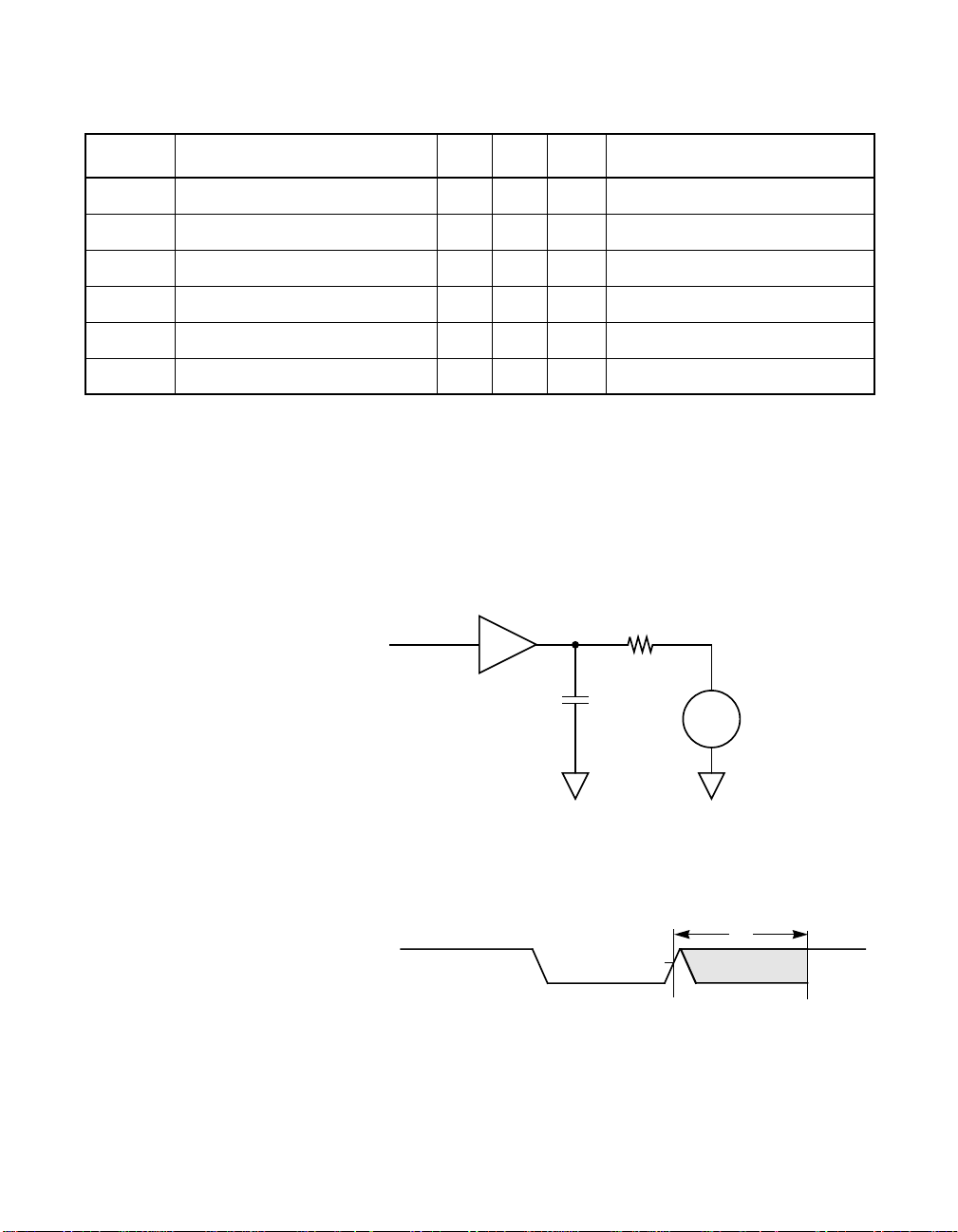
Table 3.17 TolerANT Technology Electrical Characteristics1(Cont.)
Symbol Parameter Min Max Units Test Conditions
t
F
dV
/dt Slew rate, low to high 0.15 0.49 V/ns Figure 3.3
H
dV
/dt Slew rate, high to low 0.19 0.67 V/ns Figure 3.3
L
Fall time, 90% to 10% 5.2 14.7 ns Figure 3.4
ESD Electrostatic discharge 2 – KV MIL-STD-883C; 3015-7
Latch-up 100 – mA –
t
1
Filter delay 10 15 ns Figure 3.4
1. These values are guaranteed by periodic characterization; they are not 100% tested on every device.
2. Active negation outputs only: Data, Parity, SREQ/, SACK/
3. Single pin only; irreversible damage may occur if sustained for one second.
4. SCSI RESET pin has 10 kΩ pull-up resistor.
Figure 3.3 shows the rise and fall time test conditions described in
Table 3.17.
Figure 3.3 Rise and Fall Time Test Conditions
47 Ω
20 pF
+
2.5 V
−
Figure 3.4 shows the SCSI input filtering described in Table 3.17.
Figure 3.4 SCSI Input Filtering
t
1
REQ/ or ACK/ Input
Note: t1is the input filtering period.
V
TL
Figure 3.5 shows the hysteresis of a SCSI receiver.
Electrical Characteristics 3-13
Page 44

Figure 3.5 Hysteresis of SCSI Receiver
1.1 1.3
1
Receiving Logic Level
0
1.5 1.7
Input Voltage (Volts)
Figure 3.6 shows input current as a function of input voltage.
Figure 3.6 Input Current as a Function of Input Voltage
+40
+20
0
−20
Input Current (milliAmperes)
−40
−4 0 4 8 12 16
Figure 3.7 shows output current as a function of output voltage.
3-14 Specifications
14.4 V
8.2 V
− 0.7 V
HIGH-Z
OUTPUT
ACTIVE
Input Voltage (Volts)
Page 45

Figure 3.7 Output Current as a Function of Output Voltage
0
−200
−400
−600
Output Sink Current (milliamperes)
−800
012345
Output Voltage (Volts)
3.2.3 AC Characteristics
The AC characteristics described in this section apply over the entire
range of operating conditions (refer to the DC Characteristics section).
Chip timings (Figure 3.8 on page 3-16) are based on simulation at worst
case voltage, temperature, and processing. The LSI53C120 requires a
40 MHz clock input. (See Table 3.18.)
100
80
60
40
20
0
Output Source Current (milliamperes)
012345
Output Voltage (Volts)
Table 3.18 Clock Timing
Symbol Parameter Min Max Units
t
1
t
2
t
3
t
4
Electrical Characteristics 3-15
Clock period 24.5 25.5 ns
Clock low time 10 15 ns
Clock high time 10 15 ns
Clock rise time 1 – V/ns
Page 46

Figure 3.8 Clock Timing
CLOCK
3.2.3.1 SCSI Interface Timing
Table 3.19 shows the SCSI interface input timing, Table 3.20 shows the
SCSI interface output timing, and Figure 3.9 on page 3-17 shows the
input/output timing diagram.
Table 3.19 Input Timing
Symbol Parameter Min Max Units
t
1
t
3
t
2
t
4
t
1
t
2
t
3
t
4
Input data setup 1 - ns
Input data hold 6 - ns
Input REQ/ACK assertion pulse width 11 - ns
Input REQ/ACK deassertion pulse width 16 - ns
Table 3.20 Output Timing
Symbol Parameter Min Max Units
t
5
t
6
t
7
t
8
t
9
Output data setup min [t1+ 17ns, t4+5] – ns
Output data hold max [24, (t2- 20), t3]– ns
Output REQ/ACK pulse width max [20 ns, t3-5] max [30 ns, t3+5] ns
REQ/ACK transport delay 25 ns if REQ/ACK is
clock for input data,
50 ns if REQ/ACK is clock
for input data, 30 ns if not
ns
10 ns if not
Data transport delay 6 [t3+35] ns
3-16 Specifications
Page 47

Figure 3.9 Input/Output Timing
t
3
Input Timings
REQ or ACK
t
2
t
8
Data
t
1
Valid Data
Output Timings
REQ or ACK
t
5
Valid Data
Data
t
9
3.3 LSI53C120 Mechanical Drawing
The LSI53C120 comes in a 128-pin metric Plastic Quad Flat Package
(PQFP) with a 3.9 mm footprint. See Figure 3.10 on page 3-18.
t
4
t
7
t
6
LSI53C120 Mechanical Drawing 3-17
Page 48

Figure 3.10 LSI53C120 Mechanical Drawing (Sheet 1 of 2)
Important: This drawing may not be the latest version. For board layout and manufacturing, obtain the
most recent engineering drawings from your LSI Logic marketing representative by
requesting the outline drawing for package code CT.
3-18 Specifications
Page 49

Figure 3.10 LSI53C120 Mechanical Drawing (Sheet 2 of 2)
Important: This drawing may not be the latest version. For board layout and manufacturing, obtain the
most recent engineering drawings from your LSI Logic marketing representative by
requesting the outline drawing for package code CT.
LSI53C120 Mechanical Drawing 3-19
Page 50

3-20 Specifications
Page 51

Appendix A
Differential Wiring
Diagram
Figure A.1 shows the wiring diagram for Ultra SCSI operation in the
differential mode using pull-up resistors.
LSI53C120 Ultra SCSI Bus Expander A-1
Page 52

Figure A.1 LSI53C120 Differential Wiring Diagram
LSI53C120
MSG−
SD[8:15]+
SDP1+
SD[8:15]−
SDP1−
SDP0+
SDP0−
DIFFSENS
SEL+
BSY+
RST+
SEL−
BSY−
RST−
REQ−
ACK−
C/D−
I/O−
ATN−
REQ+
ACK+
SD7+
SD6+
SD5+
SD4+
SD3+
SD2+
SD1+
SD0+
SD7−
SD6−
SD5−
SD4−
SD3−
SD2−
SD1−
SD0−
Float
Float
VDD
VDD
DIFFSENS
1.5 K
VDD
1.5 K
VDD
1.5 K
1.5 K
1.5 K
VDD
1.5 K
1.5 K
1.5 K
1.5 K
SELBSYRST-
1.5 K
SD0−
SD1−
SD2−
SD3−
SD4−
SD5−
SD6−
SD7−
SDP0−
VDD
1.5 K
SEL+
BSY+
RST+
REQ/
ACK−
MSG−
C_D−
I_O−
ATN-
DIFFSENS
SD0+
SD1+
SD2+
SD3+
SD4+
SD5+
SD6+
SD7+
SDP0+
DIFFSENS
Schottky
Diode
SN75976A2
CDE0
CDE1
CDE2
BSR
CRE
1A
1DE/RE
2A
2DE/RE
3A
3DE/RE
4A
4DE/RE
5A
5DE/RE
6A
6DE/RE
7A
7DE/RE
8A
8DE/RE
9A
9DE/RE
SN75976A2
CDE0
CDE1
CDE2
BSR
CRE
1A
1DE/RE
2A
2DE/RE
3A
3DE/RE
4A
4DE/RE
5A
5DE/RE
6A
6DE/RE
7A
7DE/RE
8A
8DE/RE
9A
9DE/RE
DIFFSENS (pin 21)
−SEL
+SEL
−BSY
+BSY
−RST
+RST
−REQ
+REQ
−ACK
+ACK
−MSG
+MSG
−C/D
+C/D
−I/O
+I/O
−ATN
+ATN
−DB0
+DB0
−DB1
+DB1
−DB2
+DB2
−DB3
+DB3
−DB4
+DB4
−DB5
+DB5
−DB6
+DB6
−DB7
+DB7
−DBP
+DBP
(42)
(41)
(34)
(33)
(38)
(37)
(46)
(45)
(36)
(35)
(40)
(39)
(44)
(43)
(48)
(47)
(30)
(29)
(4)
(3)
(6)
(5)
(8)
(7)
(10)
(9)
(12)
(11)
(14)
(13)
(16)
(15)
(18)
(17)
(20)
(19)
1B+
1B−
2B+
2B−
3B+
3B−
4B+
4B−
5B+
5B−
6B+
6B−
7B+
7B−
8B+
8B−
9B+
9B−
1B+
1B−
2B+
2B−
3B+
3B−
4B+
4B−
5B+
5B−
6B+
6B−
7B+
7B−
8B+
8B−
9B+
9B−
SCSI
Bus
A-2 Differential Wiring Diagram
Page 53

Appendix B
Glossary
ACK/ Acknowledge – Driven by an initiator, ACK/ indicates an acknowledgment
for a SCSI data transfer. In the target mode, ACK/ is received as a
response to the REQ/ Signal.
ANSI American National Standards Institute.
Arbitration The process of selecting one respondent from a collection of several
candidates that request service concurrently.
Asserted A signal is asserted when it is in the state which is indicated by the name
of the signal. Opposite of negated or deasserted.
Assertion The act of driving a signal to the true state.
Asynchronous
Transmission
ATN/ Attention – Driven by an initiator, indicates an attention condition. In the
Autoconfiguration Ports
Block A block is the basic 512 byte region of storage into which the storage
BSY/ Busy – Indicates that the SCSI Bus is being used. BSY/ can be driven
Transmission in which each byte of the information is synchronized
individually, through the use of Request (REQ/) and Acknowledge (ACK/)
signals.
target role, ATN/ is received and is responded to by entering the
Message Out Phase.
Three 8-bit ports (Address, Write_Data, and Read_Data) used by
software to access the configuration space on each Plug and Play card.
The configuration space is implemented as a set of 8-bit registers. These
registers are used by the Plug and Play software to issue commands,
check status, access the resource data information, and configure the
Plug and Play hardware.
media is divided. The Logical Block Address protocol uses sequential
block addresses to access the media.
by both the initiator and the target device.
LSI53C120 Ultra SCSI Bus Expander B-1
Page 54

Bus Acollection of unbroken signal lines that interconnect computer modules.
The connections are made by taps on the lines.
C_D/ Control/Data – Driven by a target, indicates Control or Data Information
is on the SCSI Bus. This signal is received by the initiator.
Connect The function that occurs when an initiator selects a target to start an
operation, or a target reselects an initiator to continue an operation.
Control Signals The set of nine lines used to put the SCSI bus into its different phases.
The combinations of asserted and negated control signals define the
phases.
Controller A computer module that interprets signals between a host and a
peripheral device. Often, the controller is a part of the peripheral device,
such as circuitry on a disk drive.
DB0/-DB7/ SCSI Data Bits and Parity Bit – These eight Data Bits (DB0/-DB7/), plus
a Parity Bit (DBP/), form the SCSI Bus. DB7/ is the most significant bit
and has the highest priority ID during the Arbitration Phase. Data parity
is odd. Parity is always generated and optionally checked. Parity is not
valid during arbitration.
Deasserted The act of driving a signal to the false state or allowing the cable
terminators to bias the signal to the false state (by placing the driver in
the high impedance condition).
A signal is deasserted or negated when it is in the state opposite to that
which is indicated by the name of the signal. Opposite of asserted.
Device A single unit on the SCSI bus, identifiable by an SCSI address. It can be
a processor unit, a storage unit (such as a disk or tape controller or
drive), an output unit (such as a controller or printer), or a
communications unit.
Disconnect The function that occurs when a target releases control of the SCSI bus,
allowing the bus to go to the Bus Free phase.
Driver When used in the context of electrical configuration, “driver” is the
circuitry that creates a signal on a line. When used in the context of
software, “driver” is the program that translates commands between the
initiator and target.
B-2 Glossary
Page 55

External
Configuration
All SCSI peripheral devices are external to the host enclosure.
External
Terminator
Exit-Point
Terminator
The terminator that exists on the last peripheral subsystem that
terminates the external end of the SCSI bus.
A Terminator that may be enabled or disabled which exists at the 50position high-density connector on hosts that support a mixed
configuration (combination of internal and external SCSI peripheral
devices).
Free In the context of Bus Free phase, “free” means that no SCSI device is
actively using the SCSI bus and, therefore, the bus is available for use.
Gigabyte One billion bytes; equal to one thousand megabytes.
High (logical
A signal is in the high logic state when it is above approximately 2.5 volts.
level)
Host A processor, usually consisting of the central processing unit and main
memory. Typically, a host communicates with other devices, such as
peripherals and other hosts. On the SCSI bus, a host has an SCSI
address.
Host Adapter Circuitry that translates between a processor's internal bus and a
different bus, such as SCSI. On the SCSI bus, a host adapter usually
acts as an initiator.
Initiator An SCSI device that requests another SCSI device (a target) to perform
an operation. Usually, a host acts as an initiator and a peripheral device
acts as a target.
Internal
All SCSI peripheral devices are internal to the host enclosure.
Configuration
Internal
Terminator
The terminator that exists within the host that terminates the internal end
of the SCSI bus.
I/O/ Input/Output – Driven by a target, controls the direction of data transfer
on the SCSI Bus. When active, this signal indicates input to the initiator.
When inactive, this signal indicates output from the initiator. This signal
is also used to distinguish between the Selection and Reselection
Phases.
B-3
Page 56

I/O Cycle An I/O cycle is an Input (I/O Read) operation or Output (I/O Write)
operation that accesses the PC Card’s I/O address space.
I/O Mapped A storage location or register is I/O mapped when it is available to be
accessed using I/O cycles. The register or storage location might also be
accessible using memory cycles, in which case it would also be memory
mapped.
IREQ Interrupt Request – Alerts the host computer of a condition that needs
to be serviced. Most of the interrupts are individually maskable. The
Interrupt Request signal between a PC Card and a socket when the I/O
interface is active.
LBA Abbreviation for Logical Block Address.
Logical Block
Address
A logical block address is a sequential address for accessing the blocks
on the storage media. The first block of the media is addressed as block
0 and succeeding blocks are numbered sequentially until the last block
is encountered. This is the traditional method for accessing peripherals
on an SCSI interface bus.
Logical Unit The logical representation of a physical or virtual device, addressable
through a target. A physical device can have more than one logical unit.
Low (logical
A signal is in the low logic level when it is below approximately 0.5 volts.
level)
LSB Abbreviation for Least Significant Bit or Least Significant Byte. That
portion of a number, address or field that occurs right-most when its
value is written as a single number in conventional hexadecimal or binary
notation. The portion of the number having the least weight in a
mathematical calculation using the value.
LUN Logical Unit Number. Used to identify a logical unit.
Mandatory A characteristic or feature that must be present in every implementation
of the standard.
Memory Cycle A memory cycle is a memory read (using Output Enable) operation or
memory write (using Write Enable / Program) operation that accesses
the PC Card’s common memory or attribute memory address space.
Memory
Interface
B-4 Glossary
The memory interface is the default interface after power-up, PCMCIA
Hard Reset, and PCMCIA Soft Reset for both PCMCIA cards and
Page 57

sockets. This interface supports memory operations as defined in
PCMCIA Release 1.0 and later and is used by both Memory Cards and
I/O Cards.
Memory
Mapped
A storage location or register is memory mapped when it is available to
be accessed using memory cycles. The register or storage location might
also be accessible using I/O cycles, in which it would also be I/O
mapped.
MHz Megahertz – Measurement in thousands of cycles per second. Used as
a measurement of data transfer rate.
microsecond ( s) One millionth of a second.
MSB Abbreviation for Most Significant Bit and Most Significant Byte. That
portion of a number, address or field that occurs left-most when its value
is written as a single number in conventional hexadecimal or binary
notation. The portion of the number having the most weight in a
mathematical calculation using the value.
MSG/ Message – Driven active by a target during the Message Phase. This
signal is received by the initiator.
nanosecond
One billionth of a second.
(ns)
Negated A signal is negated or deasserted when it is in the state opposite to that
which is indicated by the name of the signal. Opposite of asserted.
Negation The act of driving a signal to the false state or allowing the cable
terminators to bias the signal to the false state (by placing the driver in
the high impedance condition).
ns nanoseconds.
PC Abbreviation for Personal Computer. Often used to refer to an 80x86
based computer system.
Parity A method of checking the accuracy of binary numbers. An extra bit,
called a parity bit, is added to a number. If even parity is used, the sum
of all 1s in the number and its corresponding parity is always even. If odd
parity is used, the sum of the 1s and the parity bit is always odd.
B-5
Page 58

Peripheral
device
A device that can be attached to an SCSI bus. Typical peripheral devices
are disk drives, tape drives, printers, CD ROMs, or communications units.
Phase One of the eight states to which the SCSI bus can be set. During each
phase, different communication tasks can be performed.
Plug and Play
(PnP)
Plug and Play is a specification that frees users from locating and setting
ID and IRQ switches and jumpers. PnP permits a card to be configured
automatically after installation.
Port A connection into a bus. The SCSI bus allows eight ports.
Priority The ranking of the devices on the bus during arbitration.
Protocol A convention for data transmission that encompasses timing control,
formatting, and data representation.
Receiver The circuitry that receives electrical signals on a line.
Reconnect The function that occurs when a target reselects an initiator to continue
an operation after a disconnect.
Release The act of allowing the cable terminators to bias the signal to the false
state (by placing the driver in the high impedance condition).
REQ/ Request – Driven by a target, indicates a request for an SCSI data-
transfer handshake. This signal is received by the initiator.
Reselect A target can disconnect from an initiator in order to perform a time-
consuming function, such as a disk seek. After performing the operation,
the target can “reselect” the initiator.
RESET Reset – Clears all internal registers when active. It does not assert the
SCSI RST/ signal and therefore does not reset the SCSI bus.
RST Reset – Indicates an SCSI Bus reset condition.
SCSI Address The octal representation of the unique address (0-7) assigned to an
SCSI device. This address is normally assigned and set in the SCSI
device during system installation.
SCSI ID
(Identification)
The bit-significant representation of the SCSI address referring to one of
the signal lines DB0/ through DB7/.
or SCSI Device
ID
B-6 Glossary
Page 59

SCSI Small Computer System Interface.
SCAM An acronym for SCSI Configured AutoMagically or SCSI Configured
AutoMatically. SCAM is SCSI’s new automatic ID assignment protocol.
SCAM frees SCSI user’s from locating and setting SCSI ID switches and
jumpers. SCAM is the key part of Plug and Play SCSI.
SEL/ Select – Used by an initiator to select a target or by a target to reselect
an initiator.
Single-ended
configuration
An electrical signal configuration that uses a single line for each signal,
referenced to a ground path common to the other signal lines. The
advantage of a single-ended configuration is that it uses half the pins,
chips, and board area that differential configurations require. The main
disadvantage of single-ended configurations is that they are vulnerable
to common mode noise. Also, cable lengths are limited.
Synchronous
transmission
Transmission in which the sending and receiving devices operate
continuously at the same frequency and are held in a desired phase
relationship by correction devices. For buses, synchronous transmission
is a timing protocol that uses a master clock and has a clock period.
Target An SCSI device that performs an operation requested by an initiator.
Termination The electrical connection at each end of the SCSI bus, composed of a
set of resistors.
s Microsecond.
B-7
Page 60

B-8 Glossary
Page 61

Index
Symbols
sB-7
Numerics
3-state 2-6
3-state leakage 3-9
A
A_SACK/ 2-7, 3-4
A_SATN/ 2-8, 3-4
A_SBSY/ 2-6, 3-4
A_SCD/ 2-8, 3-4
A_SD/(15-0) 3-4
A_SDP/(1-0) 3-4
A_SIO/ 3-4
A_SMSG/ 2-8, 3-4
A_SREQ/ 2-7, 3-4
A_SRST/ 2-7, 3-4
A_SSEL/ 3-4
Absolute Maximum Stress Ratings 3-8
AC characteristics 3-15
ACK 2-7, B-1
Acknowledge 2-3
Acknowledge (ACK) 2-7
Active negation 2-3
ANSI B-1
Application examples 1-4
Arbitration B-1
Asserted B-1
Assertion B-1
Asynchronous 1-3
Asynchronous transmission B-1
ATN B-1
Attention 3-4, 3-5
Attention (ATN) 2-8
B
B_ACKDIR 2-8, 3-6
B_ATNDIR 2-8, 3-6
B_BSYDIR 2-8, 3-6
B_CD_DIR 2-8, 3-6
B_IO_DIR 2-8, 3-6
B_MSGDIR 2-8, 3-6
B_REQDIR 2-8, 3-6
B_RSTDIR 2-8, 3-6
B_SACK/ 2-7, 3-5
B_SATN/ 2-8, 3-5
B_SBSY/ 2-6, 3-5
B_SCD/ 2-8, 3-5
B_SD/(15-0) 3-5
B_SDIR(15-0) 3-6
B_SDIR(15-0, P0, P1) 2-8
B_SDIRP(1-0) 3-6
B_SDP/(1-0) 3-5
B_SELDIR 2-8, 3-6
B_SIO/ 2-8, 3-5
B_SMSG/ 2-8, 3-5
B_SREQ/ 2-7, 3-5
B_SRST/ 2-7, 3-5
B_SSEL/ 3-5
Balanced duty cycles 2-3
Bi-directional connections 2-2
Block B-1
BSY B-1
Bus B-2
Bus arbitration 3-4, 3-5
Bus Reset 3-5
Bus timings 2-4
Busy (BSY) 2-6
C
C_D B-2
Calibration 2-3
Capacitance 3-10
Card Information Structure B-2
CCS B-2
Chip Reset (RESET/) 2-10
CLOCK 3-7
Clock (CLOCK) 2-11
Clock signal 2-6
Clock Timing 3-15
Configuration 1-5, 1-6
Configurations 1-4
Connect B-2
Control Signals 3-11, B-2
Control/Data (C/D) 2-8
Controller B-2
D
D0-D7 B-2
Data 2-3, 2-5, 3-5
Data handshake 3-4, 3-5
Data parity bits 3-5
DB0-DB7 B-2
DC Characteristics 3-8
De-asserted B-2
LSI53C120 Ultra SCSI Bus Expander IX-1
Page 62

Decoupling capacitor 3-1, 3-3
Delay settings 2-3
Device B-2
DIFF_MODE 3-7
Diff_Mode Control Signal Polarity 2-9
DIFF_SENSE 3-7
Diff_Sense 3-7
Diff_Sense Control Signal Polarity 2-10
Differential control 2-1
Differential Direction Controls 2-8
Differential Mode (Diff_Mode) 2-9
Differential Sense (Diff_Sense) 2-9
Differential Signals 3-11
Disconnect B-2
Double clocking of data 2-3
Driver B-2
Driver direction control 3-6
E
EEPROM B-3
Electrostatic discharge 3-8
Enable/disable SCSI transfers 3-7
ESD 3-8
External differential transceiver 2-8
External SCSI bus 1-6
F
Filter edges 2-7
Free B-3
G
Gigabyte B-3
Glitches 2-3
H
High (logical level) B-3
Host B-3
Host Adapter B-3
Hysteresis 2-5
I
I/O B-3
I/O Cycle B-4
I/O Mapped B-4
Identification B-6
Initiator B-3
Input and Output Timings 3-16
Input capacitance of I/O pads 3-10
Input capacitance of input pads 3-10
Input high voltage 3-9
Input low voltage 3-9
Input Signals 3-10
Input Voltage 3-8
Input/Output (I/O) 2-8
Internal SCSI bus 1-6
Internal split ground system 3-1
IREQ B-4
L
Latch-up current 3-8
LBA B-4
Leading edge filter 2-7
Leading edge filtered 2-6
Lload bus 2-2
Load bus 2-5
Logical Block Address B-4
Logical Unit B-4
Low (logical level) B-4
LSB B-4
LUN B-4
M
Mandatory B-4
Master reset 3-7
Memory Cycle B-4
Memory Interface B-4
Memory Mapped B-5
Message (MSG) 2-8
MHz B-5
microsecond B-5
MSB B-5
MSG B-5
N
nanosecond B-5
Negated B-5
Negation B-5
ns B-5
O
Operating Conditions 3-9
Operating free air 3-9
Output high voltage 3-9
Output low voltage 3-9
P
Parallel function 2-7
Parity 2-3, 2-5, B-5
PC B-5
Peripheral device B-6
Phase B-6
Phase line 3-4, 3-5
Plastic Quad Flat Pack (PQFP) 3-1, 3-4, 3-5, 3-6
Port B-6
Power On Reset (POR) 2-10
Power-down 2-3
Power-up 2-3
Precision delay control 2-1
Precision delay control block 2-3
Precision delay elements 2-3
Priority B-6
Protocol B-6
Pull-down 2-6, 2-8
Pull-up 2-6, 2-8
Pulse width 2-7
IX-2 Index
Page 63

R
RC-type input filters 2-3
Receiver B-6
Receiver latch 2-6
Reconnect B-6
Recovery 2-8
Release B-6
Reliability issue 2-3
REQ 2-7, B-6
Request 2-3
Request (REQ) 2-7
Reselect B-6
Reserved B-6
RESET 2-10, B-6
Reset (RST) 2-7
RESET/ 3-7
RESET/ Control Signal Polarity 2-10
Re-timing 2-7
Re-timing circuit 2-1
Re-timing logic block 2-3
RST B-6
S
Scalable device connectivity 1-4
SCAM support 2-9
SCSI B-7
TolerANT technology 2-3
SCSI A Signal Description 3-4
SCSI Address B-6
SCSI A-side 1-4, 2-4
SCSI B-side 1-4, 2-4
SCSI bus disable mode 1-3, 1-4
SCSI bus electrical isolation 1-3, 1-6
SCSI bus protocol 2-4, 2-9
SCSI Device ID B-6
SCSI I/O logic 2-8
SCSI ID 1-3, B-6
SCSI Interface Timings 3-16
SCSI phases 2-3
SCSI Signals 3-10
SEL B-7
Signal groupings 2-4
Signal skew 2-2
Single-ended configuration B-7
Single-ended control blocks 2-1, 2-2
Single-ended to differential 1-3, 1-5, 2-4
Single-ended to single-ended 1-3, 1-5, 2-2
Software 1-3, 2-1
Source bus 2-2, 2-5
State 2-8
State machines 2-7
State-machine control 2-1
State-machine controls 2-3, 2-4
Storage temperature 3-8
Supply voltage 3-8
SYM53C120 Pin Diagram 3-1
SYM53C120 SCSI Buddy 1-1
Synchronous 1-3
Synchronous transmission B-7
Temperature 2-3
Termination B-7
Thermal resistance 3-9
TolerANT receiver technology 2-3
TolerANT SCSI 2-3
TolerANT Technology 2-3
Benefits 2-3
Electrical characteristics 3-12
TolerANT® Drivers and Receivers 2-1, 2-3
TolerANT® technology 2-3
Typical applications 1-4
U
Ultra SCSI bus 1-4
V
VDD_CORE 3-7
VDD_IO 3-7
VDD-SCSI 3-7
Vendor unique B-7
Voltage 2-3
VSS_CORE 3-7
VSS_IO 3-7
VSS-SCSI 3-7
W
Warm Start Enable and Transfer Active (WS_ENABLE and
XFER_ACTIVE) 2-10
Wide Ultra SCSI 1-3, 2-2
WS_ENABLE 3-7
WS_ENABLE Signal Polarity 2-11
X
XFER_ACTIVE 3-7
XFER_ACTIVE Signal Polarity 2-11
T
Target B-7
Index IX-3
Page 64

IX-4 Index
Page 65

Customer Feedback
We would appreciate your feedback on this document. Please copy the
following page, add your comments, and fax it to us at the number
shown.
If appropriate, please also fax copies of any marked-up pages from this
document.
Important: Please include your name, phone number, fax number, and
company address so that we may contact you directly for
clarification or additional information.
Thank you for your help in improving the quality of our documents.
LSI53C120 Ultra SCSI Bus Expander
Page 66

Reader’s Comments
Fax your comments to: LSI Logic Corporation
Technical Publications
M/S E-198
Fax: 408.433.4333
Please tell us how you rate this document: LSI53C120 Ultra SCSI Bus
Expander . Place a check mark in the appropriate blank for each category.
Excellent Good Average Fair Poor
Completeness of information ____ ____ ____ ____ ____
Clarity of information ____ ____ ____ ____ ____
Ease of finding information ____ ____ ____ ____ ____
Technical content ____ ____ ____ ____ ____
Usefulness of examples and
illustrations
Overall manual ____ ____ ____ ____ ____
____ ____ ____ ____ ____
What could we do to improve this document?
If you found errors in this document, please specify the error and page
number. If appropriate, please fax a marked-up copy of the page(s).
Please complete the information below so that we may contact you
directly for clarification or additional information.
Name Date
Telephone
Fax
Title
Department Mail Stop
Company Name
Street
City, State, Zip
Customer Feedback
Page 67

U.S. distributors, international distributors, and sales offices and design resource
centers on our web site at
http://www.lsilogic.com/contacts/na_salesoffices.html
Page 68

 Loading...