

Page 1

TECHNICAL
MANUAL
LSI53C1020/1020A
PCI-X to Ultra320
SCSI Controller
February 2004
Version 2.4
®
DB14-000176-06
Page 2

This document contains proprietary information of LSI Logic Corporation. The
information contained herein is not to be used by or disclosed to third parties
without the express written permission of an officer of LSI Logic Corporation.
LSI Logic products are not intended for use in life-support appliances, devices,
or systems. Use of any LSI Logic product in such applications without written
consent of the appropriate LSI Logic officer is prohibited.
Document DB14-000176-06, Version 2.4 (February 2004)
This document describes LSI Logic Corporation’s LSI53C1020 and
LSI53C1020A PCI-X to Ultra320 SCSI Controllers and will remain the official
reference source for all revisions/releases of these products until rescinded by an
update.
LSI Logic Corporation reserves the right to make changes to any products herein
at any time without notice. LSI Logic does not assume any responsibility or
liability arising out of the application or use of any product described herein,
except as expressly agreed to in writing by LSI Logic; nor does the purchase or
use of a product from LSI Logic convey a license under any patent rights,
copyrights, trademark rights, or any other of the intellectual property rights of
LSI Logic or third parties.
Copyright © 2001–2004 by LSI Logic Corporation. All rights reserved.
TRADEMARK ACKNOWLEDGMENT
LSI Logic, the LSI Logic logo design, Fusion-MPT, Integrated Mirroring,
Integrated RAID, Integrated Striping, LVDlink, SDMS, SureLINK, and TolerANT
are trademarks or registered trademarks of LSI Logic Corporation. ARM,
ARM966E-S, and Multi-ICE are trademarks or registered trademarks of ARM
Ltd., used under license. Windows is a registered trademarks of Microsoft
Corporation. NetWare is a registered trademarks of Novell Corporation. Linux is
a registered trademark of Linus Torvalds. Solaris is a trademark of Sun
Microsystems, Inc. SCO OpenServer is a trademark of Caldera International, Inc.
UnixWare is a trademark of The Open Group. All other brand and product names
may be trademarks of their respective companies.
KL
To receive product literature, visit us at http://www.lsilogic.com.
For a current list of our distributors, sales offices, and design resource
centers, view our web page located at
http://www.lsilogic.com/contacts/index.html
ii
Version 2.4 Copyright © 2001–2004 by LSI Logic Corporation. All rights reserved.
Page 3

Audience
Preface
This book is the primary reference and technical manual for the
LSI53C1020/1020A PCI-X to Ultra320 SCSI Controller. It contains a
functional description and electrical specifications for the
LSI53C1020/1020A.
This document assumes that you have some familiarity with
microprocessors and related support devices. The people who benefit
from this book are:
Organization
• Engineers and managers who are evaluating the LSI53C1020/1020A
for use in a system
• Engineers who are designing the LSI53C1020/1020A into a system
This document has the following chapters and appendix:
• Chapter 1, Introduction, provides an overview of the
LSI53C1020/1020A features and capabilities.
• Chapter 2, Functional Description, provides a detailed functional
description of the LSI53C1020/1020A operation. This chapter
describes how the LSI53C1020/1020A implements the PCI/PCI-X
and SCSI bus specifications.
• Chapter 3, Signal Description, provides detailed descriptions of all
LSI53C1020/1020A signals.
• Chapter 4, PCI Host Register Description, provides a bit level
description of the LSI53C1020/1020A host register set.
LSI53C1020/1020A PCI-X to Ultra320 SCSI Controller Technical Manual iii
Version 2.4 Copyright © 2001–2004 by LSI Logic Corporation. All rights reserved.
Page 4

• Chapter 5, Specifications, provides the electrical and physical
• Appendix A, Register Summary, provides a register map for the
Related Publications
LSI Logic Documents
Fusion-MPT Device Management User’s Guide, Version 2.0,
DB15-000186-02
ANSI
11 West 42nd Street
New York, NY 10036
(212) 642-4900
Global Engineering Documents
15 Inverness Way East
Englewood, CO 80112
(800) 854-7179 or (303) 397-7956 (outside U.S.) FAX (303) 397-2740
characteristics of the LSI53C1020/1020A. It also includes
LSI53C1020/1020A pinout tables and mechanical drawings.
LSI53C1020/1020A.
ENDL Publications
14426 Black Walnut Court
Saratoga, CA 95070
(408) 867-6642
Document names: SCSI Bench Reference, SCSI Encyclopedia, SCSI Tutor
Prentice Hall
113 Sylvan Avenue
Englewood Cliffs, NJ 07632
(800) 947-7700
Ask for SCSI: Understanding the Small Computer System Interface,
ISBN 0-13-796855-8
SCSI Electronic Bulletin Board
(719) 533-7950
PCI Special Interest Group
2575 N. E. Katherine
Hillsboro, OR 97214
(800) 433-5177; (503) 693-6232 (International); FAX (503) 693-8344
iv Preface
Version 2.4 Copyright © 2001–2004 by LSI Logic Corporation. All rights reserved.
Page 5

Conventions Used in This Manual
The first time a word or phrase is defined in this manual, it is italicized.
The word assert means to drive a signal true or active. The word
deassert means to drive a signal false or inactive. Signals that are active
LOW end with a “/.”
Hexadecimal numbers are indicated by the prefix “0x” —for example,
0x32CF. Binary numbers are indicated by the prefix “0b” —for example,
0b0011.0010.1100.1111.
Revision History
Revision Date Remarks
v2.4 2/2004 Corrected PCI support information and package/pin compatibility information
in Chapter 1.
v2.3 2/2004 Added 384-pin entries to signal description tables in Chapter 3.
Corrected and updated pin/signal names and ball assignments throughout
the document. Verified that this data is now consistent for the 384-pin and
456-pin packages.
Added a statement that LSI53C1020A controller supports v2.3 of the PCI
spec.
Added descriptions of the Interrupt Disable and Interrupt Status bits to the
PCI Command Register and PCI Status Register sections in Chapter 4 and
noted that the LSI53C1020A controller supports these functions.
Deleted this sentence from section 2.7: “LSI53C1020 based designs do not
use the M66EN pin to determine the PCI bus speed.” (The sentence was not
relevant, since the chip has no M66EN pin.)
Made this correction in description of Diagnostic Read/Write Address register: “The address increments by a dword whenever the host system
accesses the Diagnostic Read/Write
Data register.”
v2.2 12/2003 Updated references to Integrated RAID throughout the document.
Corrected SCSI clock, SCLK LOW, and SCLK HIGH timings in Table 5.13.
Added pinout information for 448 EPBGA and 384 EPBGA packages of the
LSI53C1020A chip. Edited descriptions of Request Queue and Reply Queue
registers (formerly called “Request FIFO” and “Reply FIFO,” respectively).
v2.1 6/2003 Updated the external memory timing diagrams.
Updated the default Subsystem ID value.
Updated the ZCR behavior description.
Updated the Multi-ICE test interface description.
Preface v
Version 2.4 Copyright © 2001–2004 by LSI Logic Corporation. All rights reserved.
Page 6

Revision Date Remarks
v2.0 4/2002 Added the register summary appendix.
Updated the electrical characteristics.
Updated the Index.
Prelim v1.0 2/2002 Updated the description of Fusion-MPT architecture in Chapter 1.
Updated the External Memory Interface descriptions in Chapter 2.
Added the Test Interface description to Chapter 2.
Added the Zero Channel RAID interface description to Chapters 2 and 3.
Updated the MAD Power-On Sense pin description in Chapter 3.
Updated the signal descriptions and lists to include the ZCR-related pins.
Updated the electrical and environmental characteristics in Chapter 5.
Removed SE SCSI electrical/timing characteristics figures from Chapter 5.
Removed SCSI timing information from Chapter 5 and referred readers to
the SCSI spec.
Removed the PSBRAM interface and all related information.
Adv v0.1 4/2001 Initial release of document.
vi Preface
Version 2.4 Copyright © 2001–2004 by LSI Logic Corporation. All rights reserved.
Page 7

Contents
Chapter 1 Introduction
1.1 General Description 1-1
1.2 Benefits of the Fusion-MPT Architecture 1-5
1.3 Benefits of PCI-X 1-6
1.4 Benefits of Ultra320 SCSI 1-7
1.5 Benefits of SureLINK (Ultra320 SCSI Domain Validation) 1-7
1.6 Benefits of LVDlink Technology 1-8
1.7 Benefits of TolerANT®Technology 1-8
1.8 Summary of LSI53C1020 Features 1-9
1.8.1 SCSI Performance 1-9
1.8.2 PCI Performance 1-10
1.8.3 Integration 1-11
1.8.4 Flexibility 1-11
1.8.5 Reliability 1-11
1.8.6 Testability 1-12
Chapter 2 Functional Description
2.1 Block Diagram Description 2-2
2.1.1 Host Interface Module Description 2-3
2.1.2 SCSI Channel Module Description 2-6
2.2 Fusion-MPT Architecture Overview 2-7
2.3 PCI Functional Description 2-8
2.3.1 PCI Addressing 2-8
2.3.2 PCI Commands and Functions 2-9
2.3.3 PCI Arbitration 2-15
2.3.4 PCI Cache Mode 2-15
2.3.5 PCI Interrupts 2-15
2.3.6 Power Management 2-16
LSI53C1020/1020A PCI-X to Ultra320 SCSI Controller Technical Manual vii
Version 2.4 Copyright © 2001–2004 by LSI Logic Corporation. All rights reserved.
Page 8

2.4 Ultra320 SCSI Functional Description 2-18
2.4.1 Ultra320 SCSI Features 2-18
2.4.2 SCSI Bus Interface 2-22
2.5 External Memory Interfaces 2-23
2.5.1 Flash ROM Interface 2-23
2.5.2 NVSRAM Interface 2-26
2.6 Serial EEPROM Interface 2-27
2.7 Zero Channel RAID 2-28
2.8 Multi-ICE Test Interface 2-29
Chapter 3 Signal Description
3.1 Signal Organization 3-2
3.2 PCI Bus Interface Signals 3-4
3.2.1 PCI System Signals 3-4
3.2.2 PCI Address and Data Signals 3-5
3.2.3 PCI Interface Control Signals 3-6
3.2.4 PCI Arbitration Signals 3-6
3.2.5 PCI Error Reporting Signals 3-7
3.2.6 PCI Interrupt Signals 3-7
3.3 PCI-Related Signals 3-8
3.4 SCSI Interface Signals 3-9
3.5 Memory Interface 3-12
3.6 Zero Channel RAID (ZCR) Interface 3-13
3.7 Test Interface 3-14
3.8 GPIO and LED Signals 3-16
3.9 Power and Ground Pins 3-16
3.10 Power-On Sense Pins Description 3-18
3.11 Internal Pull-Ups and Pull-Downs 3-22
Chapter 4 PCI Host Register Description
4.1 PCI Configuration Space Register Descriptions 4-1
Vendor ID 4-3
Device ID 4-3
Command 4-3
Status 4-5
Revision ID 4-7
Class Code 4-7
viii Contents
Version 2.4 Copyright © 2001–2004 by LSI Logic Corporation. All rights reserved.
Page 9

Cache Line Size 4-8
Latency Timer 4-8
Header Type 4-9
I/O Base Address 4-9
Memory [0] Low 4-10
Memory [0] High 4-10
Memory [1] Low 4-11
Memory [1] High 4-11
Subsystem Vendor ID 4-13
Subsystem ID 4-14
Expansion ROM Base Address 4-15
Capabilities Pointer 4-16
Interrupt Line 4-17
Interrupt Pin 4-17
Minimum Grant 4-18
Maximum Latency 4-18
Power Management Capability ID 4-19
Power Management Next Pointer 4-19
Power Management Capabilities 4-20
Power Management Control/Status 4-21
Power Management Bridge Support Extensions 4-22
Power Management Data 4-22
MSI Capability ID 4-22
MSI Next Pointer 4-23
Message Control 4-23
Message Address 4-25
Message Upper Address 4-25
Message Data 4-26
PCI-X Capability ID 4-26
PCI-X Next Pointer 4-27
PCI-X Command 4-27
PCI-X Status 4-29
4.2 I/O Space and Memory Space Register Descriptions 4-32
System Doorbell 4-34
Write Sequence 4-35
Host Diagnostic 4-36
Test Base Address 4-37
Diagnostic Read/Write Data 4-38
Contents ix
Version 2.4 Copyright © 2001–2004 by LSI Logic Corporation. All rights reserved.
Page 10

Diagnostic Read/Write Address 4-39
Host Interrupt Status 4-40
Host Interrupt Mask 4-41
Request Queue 4-42
Reply Queue 4-42
Chapter 5 Specifications
5.1 DC Characteristics 5-1
5.2 TolerANT Technology Electrical Characteristics 5-7
5.3 AC Characteristics 5-9
5.4 External Memory Timing Diagrams 5-12
5.4.1 NVSRAM Timing 5-12
5.4.2 Flash ROM Timing 5-16
5.5 Pinout Information and Mechanical Drawings 5-20
Appendix A Register Summary
Index
Customer Feedback
x Contents
Version 2.4 Copyright © 2001–2004 by LSI Logic Corporation. All rights reserved.
Page 11

Figures
1.1 Typical LSI53C1020 Board Application 1-3
1.2 Typical LSI53C1020 System Application 1-4
2.1 LSI53C1020 Block Diagram 2-3
2.2 Paced Transfer Example 2-19
2.3 Example of Precompensation 2-20
2.4 Flash ROM Block Diagram 2-25
2.5 NVSRAM Diagram 2-26
2.6 ZCR Circuit Diagram for the LSI53C1020 and
LSI53C1000R 2-29
3.1 LSI53C1020/1020A Functional Signal Grouping 3-3
5.1 LVD Driver 5-3
5.2 LVD Receiver 5-4
5.3 Rise and Fall Time Test Condition 5-8
5.4 SCSI Input Filtering 5-8
5.5 External Clock 5-9
5.6 Reset Input 5-10
5.7 Interrupt Output 5-11
5.8 NVSRAM Read Cycle 5-13
5.9 NVSRAM Write Cycle 5-15
5.10 Flash ROM Read Cycle 5-17
5.11 Flash ROM Write Cycle 5-19
5.12 LSI53C1020 456-Pin BGA Top View 5-21
5.13 LSI53C1020A 384-Pin BGA, Top View 5-26
5.14 456-Pin EPBGA (KY) Mechanical Drawing 5-31
5.15 384-Ball Count EPBGA (HT) Mechanical Drawing
(Sheet 1 of 2) 5-32
5.16 448-Ball Count EPBGA (5B) Mechanical Drawing
(Sheet 1 of 2) 5-34
Contents xi
Version 2.4 Copyright © 2001–2004 by LSI Logic Corporation. All rights reserved.
Page 12

xii Contents
Version 2.4 Copyright © 2001–2004 by LSI Logic Corporation. All rights reserved.
Page 13

Tables
2.1 PCI/PCI-X Bus Commands and Encodings 2-10
2.2 Power States 2-16
2.3 Flash ROM Size Programming 2-24
2.4 Flash Signature Value 2-26
2.5 PCI Configuration Record in Serial EEPROM 2-27
2.6 20-Pin Multi-ICE Header Pinout 2-30
3.1 PCI System Signals 3-4
3.2 PCI Address and Data Signals 3-5
3.3 PCI Interface Control Signals 3-6
3.4 PCI Arbitration Signals 3-6
3.5 PCI Error Reporting Signals 3-7
3.6 PCI Interrupt Signal 3-7
3.7 PCI-Related Signals 3-8
3.8 SCSI Bus Clock Signal 3-9
3.9 SCSI Channel Interface Signals 3-9
3.10 SCSI Channel Control Signals 3-11
3.11 Flash ROM/NVSRAM Interface Signals 3-12
3.12 Serial EEPROM Interface Signals 3-13
3.13 ZCR Configuration Signals 3-13
3.14 JTAG, ICE, and Debug Signals 3-14
3.15 LSI Logic Test Signals 3-15
3.16 GPIO and LED Signals 3-16
3.17 Power and Ground Pins 3-16
3.18 No Connect Pins 3-18
3.19 MAD Power-On Sense Pin Options 3-19
3.20 Flash ROM Size Programming 3-21
3.21 Pull-Up and Pull-Down Signal Conditions 3-22
4.1 LSI53C1020 PCI Configuration Space Address Map 4-2
4.2 Subsystem ID Register Download Conditions and Values 4-15
4.3 PCI I/O Space Address Map 4-32
4.4 PCI Memory [0] Address Map 4-33
4.5 PCI Memory [1] Address Map 4-33
5.1 Absolute Maximum Stress Ratings 5-2
5.2 Operating Conditions 5-2
Contents xiii
Version 2.4 Copyright © 2001–2004 by LSI Logic Corporation. All rights reserved.
Page 14

5.3 LVD Driver SCSI Signals – SACK±,SATN±, SBSY±,
SCD±, SD[15:0]±, SDP[1:0]±, SIO±, SMSG±, SREQ±,
SRST±, SSEL± 5-3
5.4 LVD Receiver SCSI Signals – SACK±,SATN±, SBSY±,
SCD±, SD[15:0]±, SDP[1:0]±, SIO±, SMSG±, SREQ±,
SRST±, SSEL± 5-4
5.5 DIFFSENS SCSI Signal 5-4
5.6 Input Capacitance 5-4
5.7 8 mA Bidirectional Signals – GPIO[7:0], MAD[15:0],
MADP[1:0], SerialDATA 5-5
5.8 8 mA PCI Bidirectional Signals – ACK64/, AD[63:0],
C_BE[7:0]/, DEVSEL/, FRAME/, IRDY/, PAR, PAR64,
PERR/, REQ64/, SERR/, STOP/, TRDY/ 5-5
5.9 Input Signals – CLK, DIS_PCI_FSN/, DIS_SCSI_FSN/,
GNT/, IDDTN, IDSEL, IOPD_GNT, BZRESET, BZVDD,
JtagMode, SCANEN, SCAN_MODE, SCLK, TCK_CHIP,
TCK_ICE, TESTACLK, TM, TESTHCLK, TDI_CHIP,
TDI_ICE, TMS_CHIP, TMS_ICE, TN, TRST_ICE/,
TST_RST/, ZCR_EN/ 5-6
5.10 8 mA Output Signals – ALT_INTA/, RAMWE[1:0]/,
FLSHALE[1:0]/, FLSHCE/, INTA/, RAMOE/, RAMCE/,
REQ/, RTCK_ICE, SerialCLK, TDO_CHIP, TDO_ICE 5-6
5.11 12 mA Output Signals – A_LED/, HB_LED/ 5-6
5.12 TolerANT Technology Electrical Characteristics for
SE SCSI Signals 5-7
5.13 External Clock 5-9
5.14 Reset Input 5-10
5.15 Interrupt Output 5-11
5.16 NVSRAM Read Cycle Timing 5-12
5.17 NVSRAM Write Cycle 5-14
5.18 Flash ROM Read Cycle Timing 5-16
5.19 Flash ROM Write Cycle 5-18
5.20 LSI53C1020 456-Pin Pinout by Signal Name 5-22
5.21 LSI53C1020 456-Pin Pinout by BGA Position 5-24
5.22 LSI53C1020A 384-Pin Pinout by Signal Name 5-27
5.23 LSI53C1020A 384-Pin Pinout by BGA Position 5-29
A.24 LSI53C1020 PCI Registers A-1
A.25 LSI53C1020 PCI I/O Space Registers A-3
A.26 LSI53C1020 PCI Memory [0] Registers A-4
xiv Contents
Version 2.4 Copyright © 2001–2004 by LSI Logic Corporation. All rights reserved.
Page 15

Chapter 1
Introduction
This chapter provides a general overview of the LSI53C1020/1020A
PCI-X to Ultra320 SCSI Controller. This chapter contains the following
sections:
• Section 1.1, “General Description”
• Section 1.2, “Benefits of the Fusion-MPT Architecture”
• Section 1.3, “Benefits of PCI-X”
• Section 1.4, “Benefits of Ultra320 SCSI”
• Section 1.5, “Benefits of SureLINK (Ultra320 SCSI Domain
Validation)”
• Section 1.6, “Benefits of LVDlink Technology”
• Section 1.7, “Benefits of TolerANT® Technology”
• Section 1.8, “Summary of LSI53C1020 Features”
1.1 General Description
The LSI53C1020/1020A PCI-X to Single Channel Ultra320 SCSI
Controllers bring Ultra320 SCSI performance to host adapter,
workstation, and server designs, making it easy to add a highperformance SCSI bus to any PCI or PCI-X system.
The LSI53C1020 SCSI controller is available in a 456-pin BGA package.
The LSI53C1020A SCSI controller is available in a 448-pin BGA package
that is pin-compatible with the LSI53C1020 controller and also in a
smaller 384-pin BGA package.
LSI53C1020/1020A PCI-X to Ultra320 SCSI Controller Technical Manual 1-1
Version 2.4 Copyright © 2001–2004 by LSI Logic Corporation. All rights reserved.
Page 16

The LSI53C1020 controller and the 448-pin BGA package of the
LSI53C1020A controller are pin compatible with the LSI53C1000R PCI
to Ultra160 SCSI Controller, to provide an easy and safe migration path
to Ultra320 SCSI. The LSI53C1020/1020A supports up to a 64-bit, 133
MHz PCI-X bus. The Ultra320 SCSI features for the LSI53C1020/1020A
include: double transition (DT) clocking, packetized protocol, paced
transfers, quick arbitrate and select (QAS), skew compensation,
intersymbol interference (ISI) compensation, cyclic redundancy check
(CRC), and domain validation technology. These features comply with
the American National Standard Institute (ANSI) T10 SCSI Parallel
Interface-4 (SPI-4) draft specification.
DT clocking enables the LSI53C1020/1020A to achieve data transfer
rates of up to 320 megabytes per second (Mbytes/s). Packetizedprotocol
increases data transfer capabilities with SCSI information units. QAS
minimizes SCSI bus latency by allowing the bus to directly enter the
arbitration/selection bus phase after a SCSI disconnect and skip the busfree phase. Skew compensation permits the LSI53C1020/1020A to
adjust for cable and bus skew on a per-device basis. Paced transfers
enable high-speed data transfers during DT data phases by using the
REQ/ACK transition as a free-running data clock. Precompensation
enables the LSI53C1020/1020A to adjust the signal drive strength to
compensate for the charge present on the cable. CRC improves the
SCSI data transmission integrity through enhanced detection of
communication errors. SureLINK™ Domain Validation detects the SCSI
bus configuration and adjusts the SCSI transfer rate to optimize bus
interoperability and SCSI data transfer rates. SureLINK Domain
Validation provides three levels of domain validation, assuring robust
system operation.
The LSI53C1020/1020A supports a local memory bus, which supports a
standard serial EEPROM and allows local storage of the BIOS in Flash
ROM memory. The LSI53C1020/1020A supports programming of local
Flash ROM memory for BIOS updates. Figure 1.1 shows a typical
LSI53C1020/1020A board application connected to external ROM
memory.
Note: In the rest of this document, LSI53C1020 refers to both the
1-2 Introduction
Version 2.4 Copyright © 2001–2004 by LSI Logic Corporation. All rights reserved.
LSI53C1020 SCSI controller and the LSI53C1020A SCSI
controller, unless specifically noted. Chapter 5 includes
pinout diagrams and mechanical drawings for both of these
SCSI controllers.
Page 17
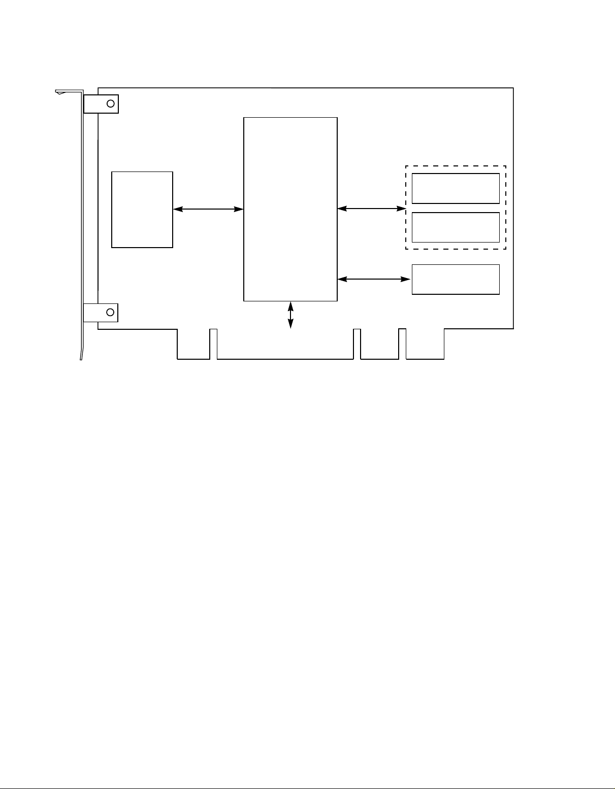
Figure 1.1 Typical LSI53C1020 Board Application
Memory Control
Block
68-PinWide SCSI
Connector
and
Terminator
Memory
Address/Data
Bus
Serial Data
Serial Clock
Flash ROM
NVSRAM
Serial EEPROM
SCSI Signals
LSI53C1020
64-Bit, 133 MHz
PCI-X to
Ultra320 SCSI
Controller
PCI-X Interface
The LSI53C1020 integrates a high-performance Ultra320 SCSI core and
a 64-bit, 133 MHz PCI-X bus master direct memory access (DMA) core.
The LSI53C1020 employs two ARM966E-S
™
processors to meet the
data transfer flexibility requirements of the Ultra320 SCSI, PCI, and PCIX specifications. Separate ARM®processors support the SCSI channel
and the PCI/PCI-X interface.
These processors implement the Fusion-MPT™ architecture, a
multithreaded I/O algorithm that supports data transfers between the host
system and SCSI devices with minimal host processor intervention.
Fusion-MPT technology provides an efficient architecture that solves the
protocol overhead problems of previous intelligent and nonintelligent
adapter designs.
LVDlink™ technology is the LSI Logic implementation of Low Voltage
Differential (LVD) SCSI. LVDlink transceivers allow the LSI53C1020 to
perform either Single-Ended (SE) or LVD transfers. Figure 1.2 illustrates
a typical LSI53C1020 system application.
General Description 1-3
Version 2.4 Copyright © 2001–2004 by LSI Logic Corporation. All rights reserved.
Page 18
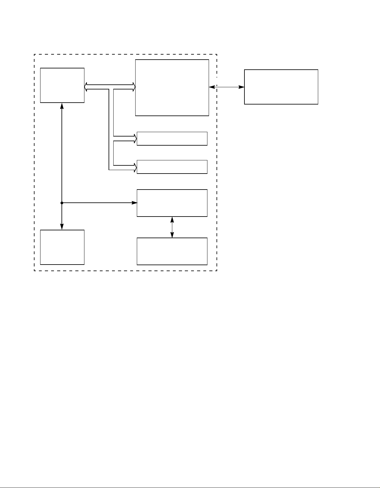
Figure 1.2 Typical LSI53C1020 System Application
LSI53C1020
PCI-X Bus
Interface
Controller
Processor Bus
Central
Processing
Unit
(CPU)
PCI-X Bus
LSI53C1020 PCI-X
to Ultra320 SCSI
PCI Graphic Accelerator
PCI Fast Ethernet
Memory
Controller
Memory
SCSI Bus
Fixed Disk, Optical Disk,
Printer, Tape, and Other
SCSI Peripherals
The LSI53C1020 supports the Integrated RAID™ solution. The
Integrated RAID solution provides cost benefits for the server or
workstation market where the extra performance, storage capacity,
and/or redundancy of a RAID configuration are required. The two
components of the Integrated RAID solution are:
• Integrated Mirroring™ (IM), which provides features of RAID 1 and
RAID 1E. The Integrated Mirroring feature provides physical
mirroring of the boot volume through LSI53C1020 firmware. This
feature provides extra reliability for the system’s boot volume without
burdening the host CPU. The runtime mirroring of the boot drive is
transparent to the BIOS, drivers, and operating system.
• Integrated Striping™ (IS), which provides features of RAID 0. The
IS feature writes data across multiple disks instead of onto one disk.
This is accomplished by partitioning each disk’s storage space into
1-4 Introduction
Version 2.4 Copyright © 2001–2004 by LSI Logic Corporation. All rights reserved.
Page 19

64 Kbyte stripes. These stripes are interleaved round-robin, so that
the combined storage space is composed alternately of stripes from
each disk.
The Fusion-MPT architecture provides the interface to the SCSI
chip/firmware to enable the Integrated Striping and Integrated Mirroring
features. LSI Logic’s CIM interface software is used to continuously
monitor IM volumes and IS volumes and to report status and error
conditions as they arise.
A BIOS-based configuration utility is provided to create the IM and IS
volumes. A DOS-based configuration utility is also provided for use on
the manufacturing floor.
For more information about the Integrated RAID solution, see the
Integrated RAID User’s Guide, DB15-000292.
1.2 Benefits of the Fusion-MPT Architecture
The Fusion-MPT architecture provides an open architecture that is ideal
for SCSI, Fibre Channel, and other emerging interfaces. The I/O interface
is interchangeable at the system and application level; embedded
software uses the same device interface for SCSI and Fibre Channel
implementations, just as application software uses the same storage
management interfaces for SCSI and Fibre Channel implementations.
LSI Logic provides Fusion-MPT device drivers that are binary compatible
between Fibre Channel and Ultra320 SCSI interfaces.
The Fusion-MPT architecture improves overall system performance by
requiring only a thin device driver, which offloads the intensive work of
managing SCSI I/Os from the system processor to the LSI53C1020.
Developed from the proven SDMS™ solution, the Fusion-MPT
architecture delivers unmatched performance of up to 50,000 Ultra320
SCSI I/Os per second with minimal system overhead or device
maintenance. The use of thin, easy-to-develop, common OS device
drivers accelerates time to market by reducing device driver development
and certification times.
The Fusion-MPT architecture provides an interrupt coalescing feature.
Interrupt coalescing allows an I/O controller to send multiple reply
messages in a single interrupt to the host processor. Sending multiple
Benefits of the Fusion-MPT Architecture 1-5
Version 2.4 Copyright © 2001–2004 by LSI Logic Corporation. All rights reserved.
Page 20

reply messages per interrupt reduces context switching of the host
processor and maximizes the host processor efficiency, which results in
a significant improvement of system performance. To use the interrupt
coalescing feature, the host processor must be able to accept and
manage multiple replies per interrupt.
The Fusion-MPT architecture also provides built-in device driver stability
because the device driver need not change for each revision of the
LSI53C1020 silicon or firmware. This architecture is a reliable, constant
interface between the host device driver and the LSI53C1020. Changes
within the LSI53C1020 are transparent to the host device driver,
operating system, and user. The Fusion-MPT architecture also saves the
user significant development and maintenance effort because it is not
necessary to alter or redevelop the device driver when a revision of the
LSI53C1020 device or firmware occurs.
1.3 Benefits of PCI-X
PCI-X doubles the maximum clock frequency of the conventional PCI
bus. The PCI-X Addendum to the PCI Local Bus Specification,
Revision 1.0a, defines enhancements to the proven PCI Local Bus
Specification, Revision 2.2. PCI-X provides more efficient data transfers
by enabling registered inputs and outputs, improves buffer management
by including transaction information with each data transfer, and reduces
bus overheadby restricting the use of wait states and disconnects. PCI-X
also reduces host processor overhead by providing a wide range of error
recovery implementations.
The LSI53C1020 supports up to a 133 MHz, 64-bit PCI-X bus and is
backward compatible with previous versions of the PCI/PCI-X bus. The
LSI53C1020 includes transaction information with all PCI-X transactions
to enable more efficient buffer management schemes. Each PCI-X
transaction contains a transaction sequence identifier (Tag), the identity
of the initiator, and the number of bytes in the sequence. The
LSI53C1020 clocks PCI-X data directly into and out of registers, which
creates a more efficient data path. The LSI53C1020 increases bus
efficiency because it does not insert wait states after the initial data
phase when acting as a PCI-X target and never inserts wait states when
acting as a PCI-X initiator.
1-6 Introduction
Version 2.4 Copyright © 2001–2004 by LSI Logic Corporation. All rights reserved.
Page 21

1.4 Benefits of Ultra320 SCSI
Ultra320 SCSI is an extension of the SPI-4 draft specification that allows
faster synchronous SCSI data transfer rates than Ultra160 SCSI. When
enabled, Ultra320 SCSI performs 160 megatransfers per second,
resulting in approximately double the synchronous data transfer rates of
Ultra160 SCSI. The LSI53C1020 performs 16-bit, Ultra320 SCSI
synchronous data transfers as fast as 320 Mbytes/s. This advantage is
most noticeable in heavily loaded systems or large block size
applications, such as video on-demand and image processing.
Ultra320 SCSI doubles both the data and clock frequencies from
Ultra160 SCSI. Due to the increased data and clock speeds,
Ultra320 SCSI introduces skew compensation and ISI compensation.
These new features simplify system design by resolving timing issues at
the chip level. Skew compensation adjusts for timing differences between
data and clock signals caused by cabling, board traces, and so on. ISI
compensation enhances the first pulse after a change in state to ensure
data integrity.
Ultra320 SCSI includes CRC, which offers higher levels of data reliability
by ensuring complete integrity of transferred data. CRC is a 32-bit
scheme, referred to as CRC-32. CRC guarantees detection of all single
or double bit errors, as well as any combination of bit errors within a
single 32-bit range.
1.5 Benefits of SureLINK (Ultra320 SCSI Domain Validation)
SureLINK Domain Validation software ensures robust SCSI interconnect
management and low-risk Ultra320 SCSI implementations by extending
the domain validation guidelines documented in the SPI-4 specifications.
Domain validation verifies that the system is capable of transferring data
at Ultra320 SCSI speeds, allowing the LSI53C1020 to renegotiate to a
lower data transfer speed and bus width if necessary. SureLINK Domain
Validation is the software control for the domain validation manageability
enhancements in the LSI53C1020. SureLINK Domain Validationsoftware
provides domain validation management at boot time as well as during
system operation.
Benefits of Ultra320 SCSI 1-7
Version 2.4 Copyright © 2001–2004 by LSI Logic Corporation. All rights reserved.
Page 22

SureLINK Domain Validation provides three levels of integrity checking
on a per-device basis: Basic (Level 1) with inquiry command; Enhanced
(Level 2) with read/write buffer; and Margined (Level 3) with margining
of drive strength and slew rates.
1.6 Benefits of LVDlink Technology
The LSI53C1020 supports LVD through LVDlink technology. This
signaling technology increases the reliability of SCSI data transfers over
longer distances than are supported by SE SCSI. The low current output
of LVD allows the I/O transceivers to be integrated directly onto the chip.
To allow the use of the LSI53C1020 in both legacy and Ultra320 SCSI
applications, this device features universal LVDlink transceivers that
support LVD SCSI and SE SCSI.
1.7 Benefits of TolerANT®Technology
The LSI53C1020 features TolerANT technology, which provides active
negation on the SCSI drivers and input signal filtering on the SCSI
receivers. Active negation causes the SCSI Request, Acknowledge,
Data, and Parity signals to be actively driven HIGH rather than passively
pulled up by terminators.
TolerANT receiver technology improves data integrity in unreliable
cabling environments where other devices would be subject to data
corruption. TolerANT receivers filter the SCSI bus signals to eliminate
unwanted transitions, without the long signal delay associated with
RC-type input filters. This improved driver and receiver technology helps
ensure correct clocking of data. TolerANT input signal filtering is a builtin feature of the LSI53C1020 and all LSI Logic Fast SCSI, Ultra SCSI,
Ultra2 SCSI, Ultra160 SCSI, and Ultra320 SCSI devices.
TolerANT technology increases noise immunity, balances duty cycles,
and improves SCSI transfer rates. In addition, TolerANT SCSI devices
do not cause glitches on the SCSI bus at power-up or power-down,
which protects other devices on the bus from data corruption. When used
with the LVDlink transceivers, TolerANT technology provides excellent
signal quality and data reliability in real world cabling environments.
1-8 Introduction
Version 2.4 Copyright © 2001–2004 by LSI Logic Corporation. All rights reserved.
Page 23

TolerANT technology is compatible with both the Alternative One and
Alternative Two termination schemes proposed by ANSI.
1.8 Summary of LSI53C1020 Features
This section provides a summary of the LSI53C1020 features and
benefits. It contains information on SCSI Performance, PCI Performance,
Integration, Flexibility, Reliability, and Testability.
1.8.1 SCSI Performance
The LSI53C1020 contains the following SCSI performance features:
• Supports Ultra320 SCSI
– Paced transfers using a free-running clock
– 320 Mbytes/s SCSI data transfer rate
– Mandatory packetized protocol
– Quick arbitrate and select (QAS)
– Skew compensation with bus training
– Transmitter precompensation to overcome ISI effects for SCSI
data signals
– Retained training information (RTI)
• Offers a performance-optimized architecture
– Two ARM966E-S processors provide high performance with low
latency
– Designed for optimal packetized performance
• Uses proven integrated LVDlink transceivers for direct attach to either
LVD or SE SCSI buses with precision-controlled slew rates
• Supports expander communication protocol (ECP)
• Uses the Fusion-MPT (Message Passing Technology) drivers to
provide full operating system support for the Windows, Linux,Solaris,
SCO OpenServer, UnixWare, OpenUnix 8, and NetWare operating
systems
Summary of LSI53C1020 Features 1-9
Version 2.4 Copyright © 2001–2004 by LSI Logic Corporation. All rights reserved.
Page 24

1.8.2 PCI Performance
The LSI53C1020 supports the following PCI features:
• Has a 133 MHz, 64-bit PCI/PCI-X interface that:
– Operates at 33 MHz or 66 MHz PCI
– Operates at up to 133 MHz PCI-X
– Supports 32-bit or 64-bit data
– Supports 32-bit or 64-bit addressing through Dual Address Cycles
(DA Cs)
– Provides a theoretical 1066 Mbytes/s zero wait state transfer rate
– Complies with PCI Local Bus Specification, Revision 2.2
(LSI53C1020) or Revision 2.3 (LSI53C1020A)
– Complies with the PCI-X Addendum to the PCI Local Bus
Specification, Revision 1.0a
– Complies with the PCI Power Management Interface
Specification, Revision 1.1
– Complies with the PC2001 System Design Guide
• Offers unmatched performance through the Fusion-MPT architecture
• Provides high throughput and low CPU utilization to offload the host
processor
• Uses SCSI Interrupt Steering Logic (SISL) to provide alternate
interrupt routing for RAID applications
• Reduces Interrupt Service Routine (ISR) overhead with interrupt
coalescing
• Supports 32-bit or 64-bit data bursts with variable burst lengths
• Supports the PCI Cache Line Size register
• Supports the PCI Memory Write and Invalidate, Memory Read Line,
and Memory Read Multiple commands
• Supports the PCI-X Memory Read Dword, Split Completion, Memory
Read Block, and Memory Write Block commands
• Supports up to eight PCI-X outstanding split transactions
• Supports Message Signaled Interrupts (MSIs)
1-10 Introduction
Version 2.4 Copyright © 2001–2004 by LSI Logic Corporation. All rights reserved.
Page 25

1.8.3 Integration
The following features make the LSI53C1020 easy to integrate:
• Is backward compatible with previous revisions of the PCI and SCSI
• 448-pin and 456-pin BGA packages are pin compatible with the
• Provides a low-risk migration path to Ultra320 SCSI from the
• Supports a full 32-bit or 64-bit PCI/PCI-X DMA bus master
• Reduces time to market with the Fusion-MPT architecture
• Provides integrated LVDlink transceivers
specifications
LSI53C1000R SCSI controller
LSI53C1000R
– Single driver binary for SCSI and Fibre Channel products
– Thin, easy to develop drivers
– Reduced integration and certification effort
1.8.4 Flexibility
The following features increase the flexibility of the LSI53C1020:
• Universal LVD transceivers are backward compatible with SE
• Provides a flexible programming interface to tune I/O performance or
• Supports MSI or pin-based (INTA/ or ALT_INTA/) interrupt signaling
• Can respond with multiple SCSI IDs
• Is compatible with 3.3 V and 5.0 V PCI signaling
1.8.5 Reliability
devices
to adapt to unique SCSI devices
– Drives and receives 3.3 V PCI signals
– Receives 5.0 V PCI if the PCI5VBIAS pin connects to 5.0 V, but
does not drive 5.0 V signals on the PCI bus
The following features enhance the reliability of the LSI53C1020:
• Supports ISI compensation
Summary of LSI53C1020 Features 1-11
Version 2.4 Copyright © 2001–2004 by LSI Logic Corporation. All rights reserved.
Page 26

• Provides 2 kV electrostatic discharge (ESD) protection on SCSI
signals
• Provides latch-up protection greater than 150 mA
• Provides voltage feed-through protection
• Supports the Integrated RAID (IR) solution to provide physical
mirroring or striping of the boot volume
• Has a high proportion of power and ground pins
• Provides power and ground isolation of I/O pads and internal chip
logic
• Supports CRC checking and generation in double transition (DT)
phases
• Provides comprehensive SureLINK Domain Validation technology:
– Basic (Level 1) with inquiry command
– Enhanced (Level 2) with read/write buffer
– Margined (Level 3) with margining of drive strength and slew
rates
• Supports TolerANT technology, which provides:
1.8.6 Testability
These features enhance the testability of the LSI53C1020:
• Allows all SCSI signals to be accessed through programmed I/O
• Supports JTAG boundary scan
• Provides ARM Multi-ICE®test interface for debugging purposes
– Active negation of SCSI Data, Parity, Request, and Acknowledge
signals for improved SCSI transfer rates
– Input signal filtering on SCSI receivers for improved data
integrity, even in noisy cabling environments
1-12 Introduction
Version 2.4 Copyright © 2001–2004 by LSI Logic Corporation. All rights reserved.
Page 27

Chapter 2
Functional Description
This chapter provides a subsytem level overview of the LSI53C1020, a
discussion of the Fusion-MPT architecture, and a functional description
of the LSI53C1020 interfaces. This chapter contains the following
sections:
• Section 2.1, “Block Diagram Description”
• Section 2.2, “Fusion-MPT Architecture Overview”
• Section 2.3, “PCI Functional Description”
• Section 2.4, “Ultra320 SCSI Functional Description”
• Section 2.5, “External Memory Interfaces”
• Section 2.6, “Serial EEPROM Interface”
• Section 2.7, “Zero Channel RAID”
• Section 2.8, “Multi-ICE Test Interface”
The LSI53C1020 is a high-performance, intelligent PCI-X to Ultra320
SCSI Controller. The LSI53C1020 controller supports the PCI Local Bus
Specification, Revision 2.2; the LSI53C1020A controller supports
Revision 2.3 of this spec. Both controllers support the PCI-X Addendum
to the PCI Local Bus Specification, Revision 1.0a and the proposed SCSI
Parallel Interface-4 (SPI-4) draft standard.
Note: In the rest of this chapter, LSI53C1020 refers to both the
LSI53C1020 SCSI controller and the LSI53C1020A SCSI
controller, unless specifically noted.
The LSI53C1020 employs the Fusion-MPT architecture to ensure robust
system performance, to support binary compatibility of host software
between the LSI Logic SCSI and Fibre Channel products, and to
significantly reduce software development time. Refer to the Fusion-MPT
Device Management User’s Guide for more information on the
LSI53C1020/1020A PCI-X to Ultra320 SCSI Controller Technical Manual 2-1
Version 2.4 Copyright © 2001–2004 by LSI Logic Corporation. All rights reserved.
Page 28

Fusion-MPT architecture and how to control the LSI53C1020 using
Fusion-MPT technology.
2.1 Block Diagram Description
The LSI53C1020 consists of two major modules: a host interface module
and an Ultra320 SCSI channel module. The modules consist of the
following components:
• Host Interface Module
– Up to a 64-bit, 133 MHz PCI/PCI-X Interface
– System Interface
– I/O Processor (IOP)
– DMA Arbiter and Router
– Shared RAM
– External Memory Interface
◊ Flash ROM Memory Controller
◊ NVSRAM
– Timer and Configuration Control
◊ Device Configuration Controller
◊ Serial EEPROM Interface Controller
◊ General Purpose I/O (GPIO) Interface
◊ Chip Timer
• Ultra320 SCSI Channel Module
– Datapath Engine
– Context Manager
– Ultra320 SCSI Core
Figure 2.1 illustrates the relationship between these modules.
2-2 Functional Description
Version 2.4 Copyright © 2001–2004 by LSI Logic Corporation. All rights reserved.
Page 29
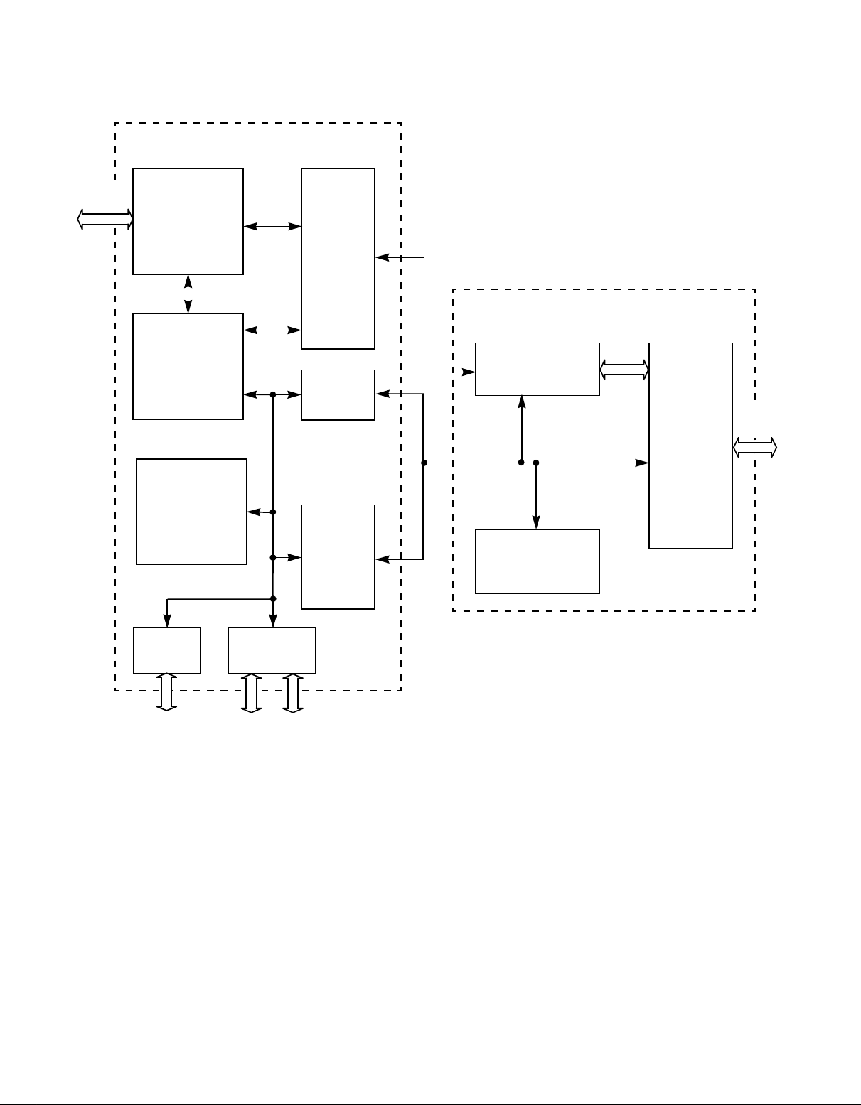
Figure 2.1 LSI53C1020 Block Diagram
Host Interface Module
PCI/
PCI-X
PCI/PCI-X
Interface
DMA
Arbiter
and
Router
SCSI Channel Module
System Interface
IOP
(ARM966E-S
Processor)
Primary Bus
External
Memory
Flash ROM/
NVSRAM
Timer, GPIO,
and EEPROM
SerialGPIO
EEPROM
Bus to Bus
Bridge
Shared
RAM
Datapath Engine
Secondary Bus
Context Manager
(ARM966E-S
Processor)
Ultra320
SCSI
Ultra320 SCSI
Core
2.1.1 Host Interface Module Description
The host interface module provides an interface between the host driver
and the SCSI channel. The host interface module controls system DMA
transfers and the host side of the Fusion-MPT architecture. It also
supports the external memory, serial EEPROM, and GPIO interfaces.
This subsection provides a detailed explanation of the host interface
submodules.
Block Diagram Description 2-3
Version 2.4 Copyright © 2001–2004 by LSI Logic Corporation. All rights reserved.
Page 30

2.1.1.1 PCI Interface
The LSI53C1020 provides a PCI-X interface that supports up to a 64-bit,
133 MHz PCI-X bus. The interface is compatible with all previous
implementations of the PCI specification. For more information on the
PCI interface, refer to Section 2.3, “PCI Functional Description,”
page 2-8.
2.1.1.2 System Interface
The system interface efficiently passes messages between the
LSI53C1020 and other I/O agents using a high-performance, packetized,
mailbox architecture. The LSI53C1020 system interface coalesces PCI
interrupts to minimize traffic on the PCI bus and maximize system
performance.
All host accesses to the IOP, external memory, and timer and
configuration subsystems pass through the system interface and use the
primary bus. The host system initiates data transactions on the primary
bus with the system interface registers. PCI Memory Space [0] and the
PCI I/O Base Address registers identify the location of the system
interface register set. Chapter 4, “PCI Host Register Description,”
provides a bit-level description of the system interface register set.
2.1.1.3 I/O Processor (IOP)
The LSI53C1020 I/O processor (IOP) is a 32-bit ARM966E-S RISC
processor. The IOP controls the system interface and uses the
Fusion-MPT architecture to manage the host side of non-DMA accesses
to the Ultra320 SCSI bus. The context manager uses the Fusion-MPT
architecture to control the SCSI side of data transfers. The IOP and
Context Manager completely manage all SCSI I/Os without host
intervention. Refer to Section 2.2, “Fusion-MPT Architecture Overview,”
page 2-7, for more information on the Fusion-MPT architecture.
2.1.1.4 DMA Arbiter and Router
The descriptor-based DMA Arbiter and Router subsystem manages the
transfer of memory blocks between local memory and the host system.
The DMA channel includes PCI bus master interface logic, the internal
bus interface logic, and a 256-byte system DMA FIFO.
2-4 Functional Description
Version 2.4 Copyright © 2001–2004 by LSI Logic Corporation. All rights reserved.
Page 31

2.1.1.5 Shared RAM
The host interface module physically contains the 96 Kbyte shared RAM.
However, both the host interface module and the SCSI channel module
access the shared RAM. The shared RAM holds a portion of the IOP and
context manager firmware, as well as the request message queue and
reply message queue. All non-DMA data transfers that use the request
and reply message queues pass through the shared RAM.
2.1.1.6 External Memory Controller
The external memory controller subsystem provides a direct interface
between the primary bus and the external memory subsystem. MAD[7:0]
and MADP[0] compose the external memory bus. The LSI53C1020
supports the Flash ROM and NVSRAM interfaces through the external
memory controller. The Flash ROM is optional if the LSI53C1020 is not
the boot device and a suitable driver exists to initialize the device. The
LSI53C1020 uses the NVSRAM for write journaling when an Integrated
Mirroring (IM) volume is defined. Write journaling is used to verify that
the mirrored disks in the IM volume are synchronized with each other.
For a detailed description of this block refer to Section 2.5, “External
Memory Interfaces,” page 2-23.
During power-up or reset the LSI53C1020 uses the MAD[15:0] and
MADP[1:0] signals as Power-On Sense pins, which configure the
LSI53C1020 through their pull-up or pull-down settings. Refer to
Section 3.10, “Power-On Sense Pins Description,” page 3-18, for a
description of the Power-On Sense pin configuration options.
2.1.1.7 Timer, GPIO, and Configuration
This subsystem provides a free-running timer to allow event time
stamping and also controls the GPIO, LED, and serial EEPROM
interfaces. The LSI53C1020 uses the free-running timer to aid in tracking
and managing SCSI I/Os. The LSI53C1020 generates the free-running
timer’s microsecond time base by dividing the SCSI reference clock by
40.
The LSI53C1020 provides eight GPIO pins (GPIO[7:0]). These pins are
under the control of the LSI53C1020 and default to the input mode upon
PCI reset. The LSI53C1020 also provides two LED pins: A_LED/ and
HB_LED/. Either firmware or hardware controls A_LED/. The
Block Diagram Description 2-5
Version 2.4 Copyright © 2001–2004 by LSI Logic Corporation. All rights reserved.
Page 32

LSI53C1020 firmware controls HB_LED/ (heartbeat LED). HB_LED/
indicates that the IOP is operational.
A 2-wire serial interface provides a connection to a nonvolatile external
serial EEPROM. The serial EEPROM stores PCI configuration
parameters for the LSI53C1020. Refer to Section 2.6, “Serial EEPROM
Interface,” page 2-27, for more information concerning the serial
EEPROM.
2.1.2 SCSI Channel Module Description
The LSI53C1020 provides one SCSI bus channel. An Ultra320 SCSI
core, a datapath engine, and a context manager support this SCSI
channel. Refer to Section 2.4, “Ultra320 SCSI Functional Description,”
page 2-18, for an operational description of the LSI53C1020 SCSI
channel.
2.1.2.1 Ultra320 SCSI Core
The Ultra320 SCSI core controls the SCSI bus interface.
2.1.2.2 Datapath Engine
The datapath engine manages the SCSI side of DMA transactions
between the SCSI bus and the host system.
2.1.2.3 Context Manager
The context manager is an ARM966E-S processor. It controls the SCSI
channel side of the LSI53C1020 Fusion-MPT architecture. The context
manager controls the outbound queues, target mode I/O mapping,
disconnect and reselect sequences, scatter/gather lists, and status
reports.
2-6 Functional Description
Version 2.4 Copyright © 2001–2004 by LSI Logic Corporation. All rights reserved.
Page 33

2.2 Fusion-MPT Architecture Overview
The Fusion-MPT architecture provides two I/O methods for the host
system to communicate with the IOP: the system interface doorbell and
the message queues.
The system interface doorbell is a simple, message-passing mechanism
that allows the PCI host system and IOP to exchange single, 32-bit
dword messages. When the host system writes to the doorbell, the
LSI53C1020 hardware generates a maskable interrupt to the IOP, which
can then read the doorbell value and take the appropriate action. When
the IOP writes a value to the doorbell, the LSI53C1020 hardware
generates a maskable interrupt to the host system. The host system can
then read the doorbell value and take the appropriate action.
There are two 32-bit message queues: the request message queue and
the reply message queue. The host uses the request queue to request
an action by the LSI53C1020, and the LSI53C1020 uses the reply queue
to return status information to the host. The request message queue
consists of only the request post FIFO. The reply message queue
consists of both the reply post FIFO and the reply free FIFO. The shared
RAM contains the message queues.
Communication using the message queues occurs through request
messages and reply messages. Request message frame descriptors are
pointers to the request message frames and are passed through the
request post FIFO. The request message frame data structure is up to
128 bytes in length and includes a message header and a payload. The
header uniquely identifies the message. The payload contains
information that is specific to the request. Reply message frame
descriptors have one of two formats and are passed through the reply
post FIFO. When indicating the successful completion of a SCSI I/O, the
IOP writes the reply message frame descriptor using the Context Reply
format, which is a message context. If a SCSI I/O does not complete
successfully, the IOP uses the Address Reply format. In this case, the
IOP pops a reply message frame from the reply free FIFO, generates a
reply message describing the error, writes the reply message to system
memory, and writes the address of the reply message frame to the reply
post FIFO. The host can then read the reply message and take the
appropriate action.
Fusion-MPT Architecture Overview 2-7
Version 2.4 Copyright © 2001–2004 by LSI Logic Corporation. All rights reserved.
Page 34

The doorbell mechanism provides both a high-priority communication
path that interrupts the host system device driver and an alternative
communication path to the message queues. Because data transport
through the system doorbell occurs a single dword at a time, use the
LSI53C1020 message queues for normal operation and data transport.
2.3 PCI Functional Description
The host PCI interface complies with the PCI Local Bus Specification,
Revision 2.2 (LSI53C1020 controller), or Revision 2.3 (LSI53C1020A
controller) and with the PCI-X Addendum to the PCI Local Bus
Specification, Revision 1.0a. The LSI53C1020 supports up to a 133 MHz,
64-bit PCI-X bus. The LSI53C1020 provides support for 64-bit
addressing with Dual Address Cycle (DAC).
2.3.1 PCI Addressing
The three physical address spaces the PCI specification defines are:
• PCI Configuration Space
• PCI I/O Space for operating registers
• PCI Memory Space for operating registers
The following sections describe the PCI address spaces.
2.3.1.1 PCI Configuration Space
The LSI53C1020 defines the PCI Configuration Space registers for the
PCI function. The configuration space is a contiguous 256 x 8-bit set of
addresses. The system BIOS initializes the configuration registers using
PCI configuration cycles. The LSI53C1020 decodes C_BE[3:0]/ to
determine if a PCI cycle intends to access the configuration register
space. The IDSEL signal behaves as a chip select signal that enables
access to the configuration register space only. The LSI53C1020 ignores
configuration read/write cycles when IDSEL is not asserted.
2.3.1.2 PCI I/O Space
The PCI specification defines I/O Space as a contiguous, 32-bit I/O
address that all system resources share, including the LSI53C1020. The
2-8 Functional Description
Version 2.4 Copyright © 2001–2004 by LSI Logic Corporation. All rights reserved.
Page 35

I/O Base Address register determines the 256-byte PCI I/O area that the
PCI device occupies.
2.3.1.3 PCI Memory Space
The LSI53C1020 contains two PCI memory spaces: PCI Memory
Space [0] and PCI Memory Space [1]. PCI Memory Space [0] supports
normal memory accesses, while PCI Memory Space [1] supports
diagnostic memory accesses. The LSI53C1020 requires 64 Kbytes of
memory space.
The PCI specification defines memory space as a contiguous, 64-bit
memory address that all system resources share. The Memory [0] Low
and Memory [0] High registers determine which 64 Kbyte memory area
PCI Memory Space [0] occupies. The Memory [1] Low and Memory [1]
High registers determine which 64 Kbyte memory area PCI Memory
Space [1] occupies.
2.3.2 PCI Commands and Functions
Bus commands indicate to the target the type of transaction the master
is requesting. The master encodes the bus commands on the C_BE[3:0]/
lines during the address phase. The PCI bus command encodings
appear in Table 2.1.
PCI Functional Description 2-9
Version 2.4 Copyright © 2001–2004 by LSI Logic Corporation. All rights reserved.
Page 36

Table 2.1 PCI/PCI-X Bus Commands and Encodings
1
C_BE[3:0]/ PCI Command PCI-X Command
Supports
as Master
Supports
as Slave
0b0000 Interrupt Acknowledge Interrupt Acknowledge No No
0b0001 Special Cycle Special Cycle No No
0b0010 I/O Read I/O Read Yes Yes
0b0011 I/O Write I/O Write Yes Yes
0b0100 Reserved Reserved N/A N/A
0b0101 Reserved Reserved N/A N/A
0b0110 Memory Read Memory Read Dword Yes Yes
0b0111 Memory Write Memory Write Yes Yes
0b1000 Reserved Alias to
Memory Read Block
0b1001 Reserved Alias to
Memory Write Block
PCI: N/A
PCI-X: No
PCI: N/A
PCI-X: No
PCI: N/A
PCI-X: Yes
PCI: N/A
PCI-X: Yes
0b1010 Configuration Read Configuration Read No Yes
0b1011 Configuration Write Configuration Write No Yes
0b1100 Memory Read Multiple Split Completion Yes Yes
2
0b1101 Dual Address Cycle Dual Address Cycle Yes Yes
0b1110 Memory Read Line Memory Read Block Yes Yes
0b1111 Memory Write and Invalidate Memory Write Block Yes Yes
2
3
1. The LSI53C1020 ignores reserved commands as a slave and never generates them as a master.
2. When acting as a slave in the PCI mode, the LSI53C1020 supports this command as the PCI Memory Read command.
3. When acting as a slave in the PCI mode, the LSI53C1020 supports this command as the PCI Memory Write command.
The following sections describe how the LSI53C1020 implements these
commands.
2.3.2.1 Interrupt Acknowledge Command
The LSI53C1020 ignores this command as a slave and never generates
it as a master.
2-10 Functional Description
Version 2.4 Copyright © 2001–2004 by LSI Logic Corporation. All rights reserved.
Page 37

2.3.2.2 Special Cycle Command
The LSI53C1020 ignores this command as a slave and never generates
it as a master.
2.3.2.3 I/O Read Command
This command reads data from an agent mapped in the I/O address
space. When decoding I/O commands, the LSI53C1020 decodes the
lower 32 address bits and ignores the upper 32 address bits. The
LSI53C1020 supports this command when operating in either the PCI or
PCI-X bus mode.
2.3.2.4 I/O Write Command
This command writes data to an agent mapped in the I/O address space.
When decoding I/O commands, the LSI53C1020 decodes the lower 32
address bits and ignores the upper 32 address bits. The LSI53C1020
supports this command when operating in either the PCI or PCI-X bus
mode.
2.3.2.5 Memory Read Command
The LSI53C1020 uses this command to read data from an agent
mapped in the memory address space. The target can perform an
anticipatory read if such a read produces no side effects. The
LSI53C1020 supports this command when operating in the PCI bus
mode.
2.3.2.6 Memory Read Dword Command
This command reads up to a single dword of data from an agent mapped
in the memory address space and can only be initiated as a 32-bit
transaction. The target can perform an anticipatory read if such a read
produces no side effects. The LSI53C1020 supports this command when
operating in the PCI-X bus mode.
2.3.2.7 Memory Write Command
This command writes data to an agent mapped in the memory address
space. The target assumes responsibility for data coherency when it
PCI Functional Description 2-11
Version 2.4 Copyright © 2001–2004 by LSI Logic Corporation. All rights reserved.
Page 38

returns “ready.” The LSI53C1020 supports this command when operating
in either the PCI or PCI-X bus mode.
2.3.2.8 Alias to Memory Read Block Command
This command is reserved for future implementations of the PCI
specification. The LSI53C1020 never generates this command as a
master.When a slave, the LSI53C1020 supports this command using the
Memory Read Block command.
2.3.2.9 Alias to Memory Write Block Command
This command is reserved for future implementations of the PCI
specification. The LSI53C1020 never generates this command as a
master.When a slave, the LSI53C1020 supports this command using the
Memory Write Block command.
2.3.2.10 Configuration Read Command
This command reads the configuration space of a device. The
LSI53C1020 never generates this command as a master, but does
respond to it as a slave. A device on the PCI bus selects the LSI53C1020
by asserting its IDSEL signal when AD[1:0] equal 0b00. During the
address phase of a configuration cycle, AD[7:2] address one of the 64
dword registers in the configuration space of each device. C_BE[3:0]/
address the individual bytes within each dword register and determine
the type of access to perform. Bits AD[10:8] address the PCI Function
Configuration Space (AD[10:8] = 0b000). The LSI53C1020 treats
AD[63:11] as logical don’t cares.
2.3.2.11 Configuration Write Command
This command writes the configuration space of a device. The
LSI53C1020 never generates this command as a master, but does
respond to it as a slave. A device on the PCI bus selects the LSI53C1020
by asserting its IDSEL signal when bits AD[1:0] equal 0b00. During the
address phase of a configuration cycle, bits AD[7:2] address one of the
64 Dword registers in the configuration space of each device. C_BE[3:0]/
address the individual bytes within each Dword register and determine
the type of access to perform. Bits AD[10:8] decode the PCI Function
Configuration Space (AD[10:8] = 0b000). The LSI53C1020 treats
AD[63:11] as logical don’t cares.
2-12 Functional Description
Version 2.4 Copyright © 2001–2004 by LSI Logic Corporation. All rights reserved.
Page 39

2.3.2.12 Memory Read Multiple Command
This command is identical to the Memory Read command, except it
additionally indicates that the master intends to fetch multiple cache lines
before disconnecting. The LSI53C1020 supports PCI Memory Read
Multiple functionality when operating in the PCI mode and determines
when to issue a Memory Read Multiple command instead of a Memory
Read command.
Burst Size Selection – The Read Multiple command reads multiple
cache lines of data during a single bus ownership. The number of cache
lines the LSI53C1020 reads is a multiple of the cache line size, which
Revision 2.2 of the PCI specification provides. The LSI53C1020 selects
the largest multiple of the cache line size based on the amount of data
to transfer.
2.3.2.13 Split Completion Command
Split transactions in PCI-X replace the delayed transactions in
conventional PCI. The LSI53C1020 supports up to eight outstanding split
transactions when operating in the PCI-X mode. A split transaction
consists of at least two separate bus transactions: a split request, which
the requester initiates, and one or more split completion commands,
which the completer initiates. Revision 1.0a of the PCI-X addendum
permits split transaction completion for the Memory Read Block, Alias to
Memory Read Block, Memory Read Dword, Interrupt Acknowledge,
I/O Read, I/O Write, Configuration Read, and Configuration Write
commands. When operating in the PCI-X mode, the LSI53C1020
supports the Split Completion command for all of these commands
except the Interrupt Acknowledge command, which the LSI53C1020
neither responds to nor generates.
2.3.2.14 Dual Address Cycles Command
The LSI53C1020 performs Dual Address Cycles (DACs), according to
the PCI Local Bus Specification, Revision 2.2. The LSI53C1020 supports
this command when operating in either the PCI or PCI-X bus mode.
2.3.2.15 Memory Read Line Command
This command is identical to the Memory Read command except it
additionally indicates that the master intends to fetch a complete cache
PCI Functional Description 2-13
Version 2.4 Copyright © 2001–2004 by LSI Logic Corporation. All rights reserved.
Page 40

line. The LSI53C1020 supports this command when operating in the PCI
mode.
2.3.2.16 Memory Read Block Command
The LSI53C1020 uses this command to read from memory. The
LSI53C1020 supports this command when operating in the PCI-X mode.
2.3.2.17 Memory Write and Invalidate Command
This command is identical to the Memory Write command, except it
additionally guarantees a minimum transfer of one complete cache line.
The master uses this command when it intends to write all bytes within
the addressed cache line in a single PCI transaction unless interrupted
by the target. This command requires implementation of the PCI Cache
Line Size register. The LSI53C1020 determines when to issue a Write
and Invalidate command instead of a Memory Write command and
supports this command when operating in the PCI bus mode.
Alignment – The LSI53C1020 uses the calculated line size value to
determine if the current address aligns to the cache line size. If the
address does not align, the LSI53C1020 bursts data using a noncache
command. If the starting address aligns, the LSI53C1020 issues a
Memory Write and Invalidate command using the cache line size as the
burst size.
Multiple Cache Line Transfers – The Memory Write and Invalidate
command can write multiple cache lines of data in a single bus
ownership. The LSI53C1020 issues a burst transfer as soon as it
reaches a cache line boundary. The PCI Local Bus specification states
that the transfer size must be a multiple of the cache line size. The
LSI53C1020 selects the largest multiple of the cache line size based on
the transfer size. When the DMA buffer contains less data than the value
Cache Line Size register specifies, the LSI53C1020 issues a Memory
Write command on the next cache boundary to complete the data
transfer.
2.3.2.18 Memory Write Block Command
The LSI53C1020 uses this command to burst data to memory. The
LSI53C1020 supports this command when operating in the PCI-X bus
mode.
2-14 Functional Description
Version 2.4 Copyright © 2001–2004 by LSI Logic Corporation. All rights reserved.
Page 41

2.3.3 PCI Arbitration
The LSI53C1020 contains a bus mastering function for the SCSI function
and for the system interface. The system interface bus mastering
function manages DMA operations as well as the request and reply
message frames. The SCSI channel bus mastering functions manage
data transfers across the SCSI channel.
The LSI53C1020 uses a REQ/-GNT/ signal pair to arbitrate for access to
the PCI bus. To ensure fair access to the PCI bus, the internal arbiter
uses a round robin arbitration scheme to decide which of the two internal
bus mastering functions can arbitrate for access to the PCI bus.
2.3.4 PCI Cache Mode
The LSI53C1020 supports an 8-bit Cache Line Size register. The
Cache Line Size register provides the ability to sense and react to
nonaligned addresses corresponding to cache line boundaries. The
LSI53C1020 determines when to issue a PCI cache command (Memory
Read Line, Memory Read Multiple, and Memory Write and Invalidate), or
PCI noncache command (Memory Read or Memory Write command).
2.3.5 PCI Interrupts
The LSI53C1020 signals an interrupt to the host processor either using
PCI interrupt pins, INTA/ and ALT_INTA/, or using Message Signaled
Interrupts (MSIs). If using the PCI interrupt pins, the Interrupt Request
Routing Mode bits in the Host Interrupt Mask register configure the
routing of each interrupt to either the INTA/ and/or the ALT_INTA/ pin.
If using MSI, the LSI53C1020 does not signal interrupts on INTA/ or
ALT_INTA/. Note that enabling MSI to mask PCI interrupts is a violation
of the PCI specification. The LSI53C1020 supports one requested
message and disables MSI after the chip powers up or resets.
The Host Interrupt Mask register also prevents the assertion of a PCI
interrupt to the host processor by selectively masking reply interrupts and
system doorbell interrupts. This register masks both pin-based and MSIbased interrupts.
PCI Functional Description 2-15
Version 2.4 Copyright © 2001–2004 by LSI Logic Corporation. All rights reserved.
Page 42

2.3.6 Power Management
The LSI53C1020 complies with the PCI Power Management Interface
Specification, Revision 1.1, and the PC2001 System Design Guide. The
LSI53C1020 supports the D0, D1, D2, D3
D0 is the maximum power state, and D3 is the minimum power state.
Power State D3 is further categorized as D3
function off places it in the D3
Bits [1:0] of the Power Management Control/Status register
independently control the power state of the PCI device on the
LSI53C1020. Table 2.2 provides the power state bit settings.
Table 2.2 Power States
Power Management Control
and Status Register, Bits [1:0] Power State Function
, and D3
hot
or D3
hot
power state.
cold
0b00 D0 Maximum Power
0b01 D1 Snooze Mode
power states.
cold
. Powering the
cold
The following sections describe the PCI Function Power States D0, D1,
D2, and D3. As the device transitions from one power level to a lower
one, the attributes that occur in the higher power state level carry into
the lower power state level. For example, Power State D2 includes the
attributes for Power State D1, as well as the attributes defined for Power
State D2. The following sections describe the PCI Function power states
in conjunction with the SCSI function.
2.3.6.1 Power State D0
Power State D0 is the maximum power state and is the power-up default
state for each function. The LSI53C1020 is fully functional in this state.
2.3.6.2 Power State D1
According to the PCI Power Management Interface Specification, Power
State D1 must have a power level equal to or lower than Power State D0.
0b10 D2 Coma Mode
0b11 D3 Minimum Power
2-16 Functional Description
Version 2.4 Copyright © 2001–2004 by LSI Logic Corporation. All rights reserved.
Page 43

A function in Power State D1 places the SCSI core in the snooze mode.
In the snooze mode, a SCSI reset does not generate an IRQ/ signal.
2.3.6.3 Power State D2
According to the PCI Power Management Interface Specification, Power
State D2 must have a power level equal to or lower than Power State D1.
A function in this state places the SCSI core in the coma mode. Placing
the PCI Function in Power State D2 disables the SCSI and DMA
interrupts, and suppresses the following PCI Configuration Space
Command register enable bits:
• I/O Space Enable
• Memory Space Enable
• Bus Mastering Enable
• SERR/Enable
• Enable Parity Error Response
Therefore, the memory and I/O spaces in a function cannot be accessed,
and the PCI function cannot be a PCI bus master.
If the PCI function is changed from Power State D2 to Power State D1
or Power State D0, the PCI function restores the previous values of the
PCI Command register and asserts any interrupts that were pending
before the function entered Power State D2.
2.3.6.4 Power State D3
According to the PCI Power Management Interface Specification, Power
State D3 must have a power level equal to or lower than Power State D2.
Power State D3 is the minimum power state and includes the D3
D3
cold
D3
cold
by applying VCC and resetting the device.
Placing a function in Power State D3 puts the LSI53C1020 core in the
coma mode, clears the PCI Command register, and continually asserts
the function's soft reset. Asserting soft reset clears all pending interrupts
and 3-states the SCSI bus.
settings. D3
allows the device to transition to D0 using software.
hot
removes power from the LSI53C1020. D3
can transition to D0
cold
hot
and
PCI Functional Description 2-17
Version 2.4 Copyright © 2001–2004 by LSI Logic Corporation. All rights reserved.
Page 44

2.4 Ultra320 SCSI Functional Description
The Ultra320 SCSI channel supports wide SCSI synchronous transfer
rates up to 320 Mbytes/s across an SE or LVD SCSI bus. The integrated
LVDlink transceivers support both LVD and SE signals and do not require
external transceivers. The LSI53C1020 supports the Ultra320 SCSI,
Ultra160 SCSI, Ultra2 SCSI, Ultra SCSI, and Fast SCSI interfaces.
2.4.1 Ultra320 SCSI Features
This section describes how the LSI53C1020 implements the features in
the SPI-4 draft specification.
2.4.1.1 Parallel Protocol Request (PPR)
A SCSI extended message negotiates the PPR parameters. The PPR
parameters include the (1) transfer period; (2) maximum REQ/ACK
offset; (3) QAS; (4) margin control settings (MCS); (5) transfer width;
(6) IU_Request; (7) write flow; (8) read streaming; (9) RTI;
(10) precompensation enable; (11) information unit transfers; and the
(12) DT data phases between an initiator and a target.
2.4.1.2 Double Transition (DT) Clocking
Ultra160 SCSI and Ultra320 SCSI implement DT clocking to provide
speeds up to 80 megatransfers per second (megatransfers/s) for
Ultra160 SCSI, and up to 160 megatransfers/s for Ultra320 SCSI. When
implementing DT clocking, a SCSI device samples data on both the
asserting and deasserting edge of REQ/ACK. DT clocking is only valid
using an LVD SCSI bus.
2.4.1.3 Intersymbol Interference (ISI) Compensation
ISI Compensation uses paced transfers and precompensation to enable
high data transfer rates. Ultra320 SCSI data transfers require
ISI Compensation.
Paced Transfers – The initiator and target must establish a paced
transfer agreement that specifies the REQ/ACK offset and the transfer
period before using this feature. Devices can only perform paced
transfers during Ultra320 SCSI DT data phases. In paced transfers, the
2-18 Functional Description
Version 2.4 Copyright © 2001–2004 by LSI Logic Corporation. All rights reserved.
Page 45

device sourcing the data drives the REQ/ACK signal as a free-running
clock. The transition of the REQ/ACK signal, either the assertion or the
negation, clocks data across the bus. For successful completion of a
paced transfer, the number of ACK transitions must equal the number of
REQ transitions and both the REQ and ACK lines must be negated.
The P1 line indicates valid data in 4-byte quantities by using its phase.
The transmitting device indicates the start of valid data state by holding
the state of the P1 line for the first two data transfer periods. Beginning
on the third data transfer period, the transmitting device continues the
valid data state by toggling the state of the P1 line every two data transfer
periods for as long as the data is valid. The transmitting device must
toggle the P1 line coincident with the REQ/ACK assertion. The method
provides a minimum data valid period of two transfer periods.
To pause the data transfer, the transmitting device reverses the phase of
P1 by withholding the next transition of P1 at the start of the first two
invalid data transfer periods. Beginning with the third invalid data transfer
period, the transmitting device toggles the P1 line every two invalid data
transfer periods until it sends valid data. The transmitting device returns
to the valid data state by reversing the phase of the P1 line. The invalid
data state must experience at least one P1 transition before returning to
the valid data state. This method provides a minimum data invalid period
of four transfer periods.
Figure 2.2 provides a waveform diagram of paced data transfers and
illustrates the use of the P1 line.
Figure 2.2 Paced Transfer Example
Data Not ValidData Valid Data Valid Data Not Valid
REQ
ACK
P1
DA TA
The LSI53C1020 uses the PPR negotiation that the SPI-4 draft standard
describes to establish a paced transfer agreement for each
initiator-target pair.
Ultra320 SCSI Functional Description 2-19
Version 2.4 Copyright © 2001–2004 by LSI Logic Corporation. All rights reserved.
Page 46

Precompensation – When transmitting in the Ultra320 SCSI mode, the
LSI53C1020 uses precompensation to adjust the strength of the REQ,
ACK, parity, and data signals. When a signal transitions to HIGH or LOW,
the LSI53C1020 boosts the signal drive strength for the first data transfer
period, and then lowers the signal drive strength on the second data
transfer period if the signal remains in the same state. The LSI53C1020
maintains the lower signal drive strength until the signal again transitions
HIGH or LOW. Figure 2.3 illustrates the drivers performance with
precompensation enabled and disabled.
Figure 2.3 Example of Precompensation
a. Drivers with Precompensation Disabled
Normal Drive Strength
b. Drivers with Precompensation Enabled
Boosted Drive Strength
2.4.1.4 Packetized Transfers
Packetized transfers are also referred to as information unit transfers.
They reduce overhead on the SCSI bus by merging several of the SCSI
bus phases. Packetized transfers can only occur in DT Data phases. The
initiator and target must establish either a DT synchronous transfer
Normal Drive Strength
2-20 Functional Description
Version 2.4 Copyright © 2001–2004 by LSI Logic Corporation. All rights reserved.
Page 47

agreement or a paced transfer agreement before performing packetized
transfers.
The number of bytes in an information unit transfer is always a multiple
of four. If the number of bytes to transfer in the information unit is not a
multiple of four, the LSI53C1020 transmits pad bytes to bring the byte
count to a multiple of four.
2.4.1.5 Quick Arbitration and Selection (QAS)
When using packetized transfers, QAS allows devices to arbitrate for the
bus immediately after the message phase. QAS reduces the bus
overhead and maximizes bus bandwidth by skipping the bus free phase
that normally follows a SCSI connection.
To perform QAS, the target sends a QAS request message to the initiator
during the message phase of the bus. QAS-capable devices snoop the
SCSI bus for the QAS request message. If a QAS request message is
seen, devices can immediately move to the arbitration phase without
going to the bus free phase. The LSI53C1020 employs a fairness
algorithm to ensure that all devices have equal bus access.
2.4.1.6 Skew Compensation
The LSI53C1020 provides a method to account for and control system
skew between the clock and data signals. Skew compensation is only
available when the device operates in the Ultra320 SCSI mode. The
initiator-target pair uses the training sequences in the SPI-4 draft
standard to determine the skew compensation. Depending on the state
of the RTI bit in the PPR negotiation, the LSI53C1020 can either execute
this training pattern during each connection, or can execute the training
pattern, store the adjustment parameters, and recall them on subsequent
connections with the given device. The target determines when to
execute the training pattern.
2.4.1.7 Cyclic Redundancy Check (CRC)
Ultra320 SCSI and Ultra160 SCSI devices employ CRC as an error
detection code during the DT Data phases. These devices transfer four
CRC bytes during the DT Data phases to ensure reliable data transfers.
Ultra320 SCSI Functional Description 2-21
Version 2.4 Copyright © 2001–2004 by LSI Logic Corporation. All rights reserved.
Page 48

2.4.1.8 SureLINK Domain Validation
SureLINK Domain Validation establishes the integrity of a SCSI bus
connection between an initiator and a target. Under the SureLINK
Domain Validation procedure, a host queries a device to determine its
ability to communicate at the negotiated data transfer rate.
SureLINK Domain Validation provides three levels of integrity checking:
Basic (Level 1) with inquiry command; Enhanced (Level 2) with
read/write buffer; and Margined (Level 3) with drive strength margining
and slew rate control. The basic check consists of an inquiry command
to detect gross problems. The enhanced check sends a known data
pattern using the read and write buffer commands to detect additional
problems. The margined check verifies that the physical parameters have
a reasonable operating margin. Use SureLINK Domain Validation only
during the diagnostic system checks and not during normal system
operation. If transmission errors occur during any of these checks, the
system can reduce the transmission rate on a per-target basis to ensure
robust system operation.
2.4.2 SCSI Bus Interface
This section describes the SCSI bus modes that the LSI53C1020
supports and the SCSI bus termination methods necessary to operate a
high speed SCSI bus.
2.4.2.1 SCSI Bus Modes
The LSI53C1020 supports SE and LVD transfers. To increase device
connectivity and SCSI cable length, the LSI53C1020 features LVDlink
technology, which is the LSI Logic implementation of LVD SCSI. LVDlink
transceivers provide the inherent reliability of differential SCSI and a
long-term migration path for faster SCSI transfer rates.
The DIFFSENS signal detects the different input voltages for HVD, LVD,
and SE. The LSI53C1020 drivers are tolerant of HVD signal strengths,
but do not support the HVD bus mode. The LSI53C1020 SCSI device
3-states its SCSI drivers when it detects an HVD signal level.
2-22 Functional Description
Version 2.4 Copyright © 2001–2004 by LSI Logic Corporation. All rights reserved.
Page 49

2.4.2.2 SCSI Termination
The terminator networks pull signals to an inactive voltage level and
match the impedance seen at the end of the cable to the characteristic
impedance of the cable. Install terminators at the extreme ends of the
SCSI chain, and only at the ends; all SCSI buses must have exactly two
terminators.
Note: If using the LSI53C1020 in a design with an 8-bit SCSI bus,
designers must terminate all 16 data lines.
2.5 External Memory Interfaces
The LSI53C1020 provides Flash ROM, NVSRAM, and serial EEPROM
interfaces. The Flash ROM interface stores the SCSI BIOS and firmware
image. The Flash ROM is optional if the LSI53C1020 is not the boot
device and a suitable driver exists to initialize the LSI53C1020. Integrated
Mirroring (IM) technology requires an NVSRAM for write journaling. The
nonvolatile external serial EEPROM stores configuration parameters for
the LSI53C1020.
2.5.1 Flash ROM Interface
The Flash ROM interface multiplexes the 8-bit address and data buses
on the MAD[7:0] pins. The interface latches the address into three 8-bit
latches to support up to 1 Mbyte of address space. The interface
supports byte, word, and dword accesses. The LSI53C1020 dword aligns
dword reads, word aligns word reads, and byte aligns byte reads. The
remaining bits from word and byte reads are meaningless.
The MAD[2:1] Power-On Sense pin configurations define the size of the
Flash ROM address space. Table 2.3 provides the pin encoding for these
External Memory Interfaces 2-23
Version 2.4 Copyright © 2001–2004 by LSI Logic Corporation. All rights reserved.
Page 50

pins. By default, internal logic pulls these pins down to indicate that no
Flash ROM is present.
Table 2.3 Flash ROM Size Programming
MAD[2:1] Options Flash ROM Size
0b00 No Flash ROM present (Default)
0b01 Up to 1024 Kbytes
0b10
Reserved
0b11
1. Choose this setting for a 128 Kbyte or 512 Kbyte Flash ROM.
1
The LSI53C1020 defines only the middle (MA[15:8]) and lower (MA[7:0])
address ranges if the Flash ROM addressable space is 64 Kbytes or
less. The LSI53C1020 defines the upper (MA[21:16]), middle (MA[15:8]),
and lower (MA[7:0]) address ranges if the Flash ROM addressable space
is 128 Kbytes or more. Figure 2.4 provides an example of a Flash ROM
configuration.
2-24 Functional Description
Version 2.4 Copyright © 2001–2004 by LSI Logic Corporation. All rights reserved.
Page 51
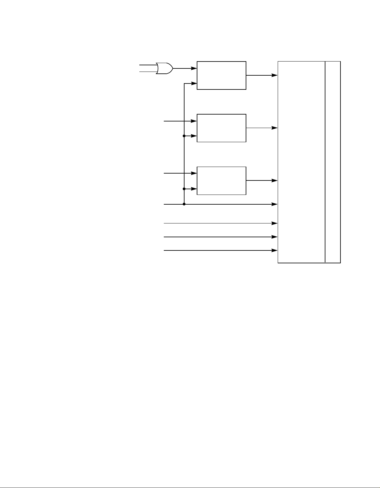
Figure 2.4 Flash ROM Block Diagram
Upper Address
FLSHALE[1]/
FLSHALE[0]/
CK
D
Middle Address
Q
A[21:16]
FLSHALE[1]/
FLSHALE[0]/
MAD[7:0]
FLSHCE/
RAMOE/
RAMWE[0]/
CK
D
Lower Address
CK
D
Q
Q
A[15:8]
A[7:0]
Flash ROM (512 K x 8)
D[7:0]
CE/
OE/
WE/
The LSI53C1020 implements a Flash signature recognition mechanism
to determine if the Flash contains a valid image. The Flash can be
present and not contain a valid image either before its initial
programming or during board testing. The first access to the Flash is a
16-byte burst read beginning at Flash address 0x000000. The
LSI53C1020 compares the values read to the Flash signature values that
Table 2.4 provides. If the signature values match, the LSI53C1020
performs the instruction located at Flash address 0x000000. If the
signature values do not match, the LSI53C1020 records an error and
ignores the Flash instruction. The Flash signature does not include the
first three bytes of Flash memory because these bytes contain a branch
offset instruction.
External Memory Interfaces 2-25
Version 2.4 Copyright © 2001–2004 by LSI Logic Corporation. All rights reserved.
Page 52
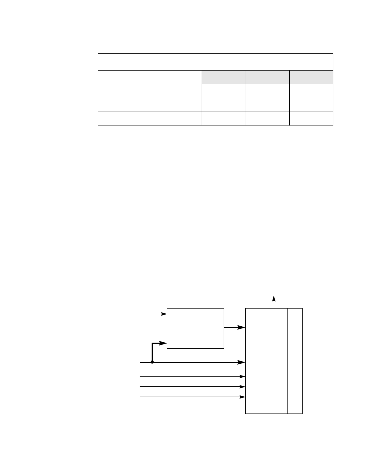
Table 2.4 Flash Signature Value
Flash Address Flash Signature Values
Bytes [3:0] 0xEA
Bytes [7:4] 0x5A 0xEA 0xA5 0x5A
Bytes [11:8] 0xA5 0x5A 0xEA 0xA5
Bytes [15:12] 0x5A 0xA5 0x5A 0xEA
2.5.2 NVSRAM Interface
The LSI53C1020 Fusion-MPT firmware is capable of maintaining an
Integrated Mirroring (IM) volume of the boot drive. IM firmware requires
a 32 Kbyte NVSRAM in order to perform write journaling. Write journaling
is used to verify that the mirrored disks in the IM volume are
synchronized with each other. The NVSRAM also stores additional code
and data used for error and exception handling, and it stores IM
configuration information during serial EEPROM updates. The disk write
log uses approximately 4 Kbytes of the NVSRAM.
Figure 2.5 provides a block diagram illustrating how to connect the
NVSRAM. This design employs the CPLD to latch the address instead
of using separate address latches.
XX XX XX
Figure 2.5 NVSRAM Diagram
FLSHALE[1:0]/
MAD[7:0]
RAMCE/
RAMOE/
RAMWE[0]/
2-26 Functional Description
Version 2.4 Copyright © 2001–2004 by LSI Logic Corporation. All rights reserved.
CPLD
CY37032
MAS[1:0]
MAD[7:0]
MAD[14:0]
A[14:0]
D[7:0]
CE/
OE/
WE/
3.3 V
NVSRAM (32 K x 8)
Page 53

When using an NVSRAM, pull the MAD[3] Power-On Sense pin HIGH
during board boot-up. This configures the external memory interface as
an NVSRAM interface. During operation, RAMCE/ selects the NVSRAM
when MAD[3] is pulled HIGH.
2.6 Serial EEPROM Interface
The nonvolatile external serial EEPROM stores configuration fields for
the LSI53C1020. The serial EEPROM contains fields for the Subsystem
ID, Subsystem Vendor ID, and the size of the PCI Diagnostic Memory
Space. The LSI53C1020 must establish each of these parameters prior
to reading system BIOS and loading the PCI Configuration Space
registers. The power-on option settings enable the download of PCI
configuration data from the serial EEPROM. For more information on the
setting of the power-on options, refer to Section 3.10, “Power-On Sense
Pins Description,” page 3-18.
A 2-wire serial interface provides the connection to the serial EEPROM.
During initialization, the firmware checks if a serial EEPROM exists.
Firmware uses the checksum byte to determine if the configuration held
in the serial EEPROM is valid. If the checksum fails, the firmware checks
for a valid NVData signature. If a valid NVData signature is found, the
firmware individually checksums each persistent configuration page to
find the invalid page or pages. Table 2.5 provides the structure of the
configuration record in the serial EEPROM.
Table 2.5 PCI Configuration Record in Serial EEPROM
EEPROM Address Configuration Data
0x00 Subsystem ID, bits [7:0]
0x01 Subsystem ID, bits [15:8]
0x02 Subsystem Vendor ID, bits [7:0]
0x03 Subsystem Vendor ID, bits [15:8]
0x04 PCI Diagnostic Memory Size
0x05–0x09 Reserved
0x0A Checksum
Serial EEPROM Interface 2-27
Version 2.4 Copyright © 2001–2004 by LSI Logic Corporation. All rights reserved.
Page 54

2.7 Zero Channel RAID
Zero channel RAID (ZCR) capabilities enable the LSI53C1020 to
respond to accesses from a PCI RAID controller card or chip that is able
to generate ZCR cycles. The LSI53C1020 ZCR functionality is controlled
through the ZCR_EN/ and the IOPD_GNT signals. Both of these signals
have internal pull-ups and are active LOW.
The ZCR_EN/ signal enables ZCR support on the LSI53C1020. Pulling
ZCR_EN/ HIGH disables ZCR support on the LSI53C1020 and causes
the LSI53C1020 to behave as a normal PCI-X to Ultra320 SCSI
controller. When ZCR is disabled, the IOPD_GNT signal has no effect on
the LSI53C1020 operation.
Pulling ZCR_EN/ LOW enables ZCR operation. When ZCR is enabled,
the LSI53C1020 responds to PCI configuration cycles when the
IOPD_GNT and IDSEL signal are asserted. Connect the IOPD_GNT pin
on the LSI53C1020 to the PCI GNT/ signal of the external I/O processor.
This allows the I/O processor to perform PCI configuration cycles to the
LSI53C1020 when the I/O processor is granted the PCI bus. This
configuration also prevents the system processor from accessing the
LSI53C1020 PCI configuration registers.
Figure 2.6 illustrates how to connect the LSI53C1020 to enable ZCR.
This figure also contains information for connecting the
LSI53C1000R-based designs to a ZCR design and migrating from
LSI53C1000R-based designs to LSI53C1020-based designs. Notice that
the LSI53C1020 does not require the 2:1 mux.
2-28 Functional Description
Version 2.4 Copyright © 2001–2004 by LSI Logic Corporation. All rights reserved.
Page 55
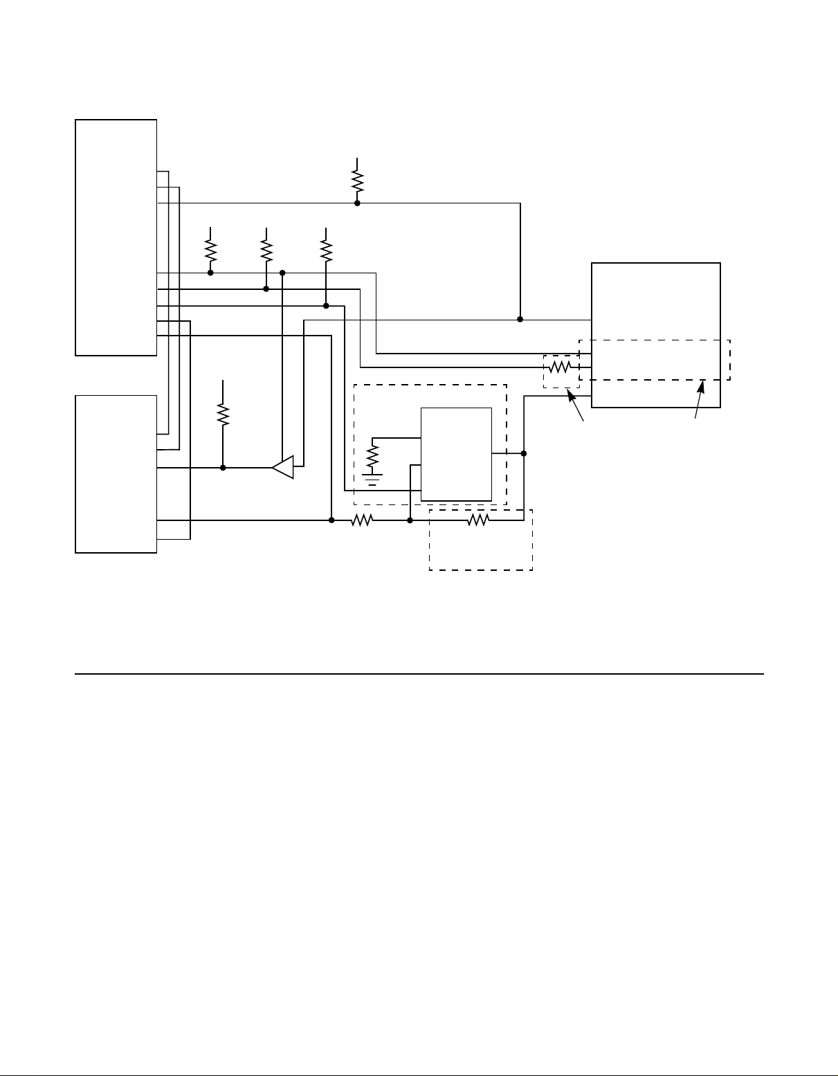
Figure 2.6 ZCR Circuit Diagram for the LSI53C1020 and LSI53C1000R
ZCR PCI
Slot
Vdd
Int A/ (A6)
Int B/ (B7)
Int C/ (A7)
Int D/ (B8)
TDI (A4)
GNT/ (A17)
TMS (A3)
IDSEL (A26)
AD21 (B29)
Host System
Int A/
Int B/
Int C/
Int D/
AD21
AD19
Vdd
4.7 kΩ
Vdd
Vdd
0.1 kΩ
4.7 kΩ
Vdd
0.1 kΩ
4.7 kΩ
No Pop for LSI53C1020
0.1 kΩ
220 Ω
2:1 Mux
A0
A1
S0
B0
0 Ω
No Pop for
LSI53C1000R
INTA/
ZCR_EN/
IOPD_GNT
0 Ω
IDSEL
No Pop for
LS53C1000R
LSI53C1000R/
LSI53C1020
LSI53C1020 Only
Note: To maintain proper interrupt mapping, select the address line for use as IDSEL on the
LSI53C1000R/LSI53C1020 to be +2 address lines above IDSEL on ZCR slot.
2.8 Multi-ICE Test Interface
This section describes the LSI Logic requirements for the Multi-ICE test
interface. LSI Logic recommends routing all test signals to a header on
the board.
The Multi-ICE test interface header is a 20-pin header for Multi-ICE
debugging through the ICE JTAG port. This header is essential for
debugging both the firmware and the design functionality and must be
included in board designs. The connector is a 20-pin header that mates
with the IDC sockets mounted on a ribbon cable. Table 2.6 details the
pinout of the 20-pin header.
Multi-ICE Test Interface 2-29
Version 2.4 Copyright © 2001–2004 by LSI Logic Corporation. All rights reserved.
Page 56

Table 2.6 20-Pin Multi-ICE Header Pinout
Pin Number Signal Pin Number Signal
1 VDD 2 VDD
3 TRST_ICE/
5 TDI_ICE
7 TMS_ICE
9 TCK_ICE
1
1
1
1
4 VSS
6 VSS
8 VSS
10 VSS
11 RTCK_ICE 12 VSS
13 TDO_ICE 14 VSS
15 No Connect 16 VSS
17 No Connect 18 VSS
19 No Connect 20 VSS
1. The designer must connect a 4.7 kΩ resistor from this signal to 3.3 V.
2-30 Functional Description
Version 2.4 Copyright © 2001–2004 by LSI Logic Corporation. All rights reserved.
Page 57

Chapter 3
Signal Description
This chapter describes the input and output signals of the LSI53C1020.
This chapter contains the following sections:
• Section 3.1, “Signal Organization”
• Section 3.2, “PCI Bus Interface Signals”
• Section 3.3, “PCI-Related Signals”
• Section 3.4, “SCSI Interface Signals”
• Section 3.5, “Memory Interface”
• Section 3.6, “Zero Channel RAID (ZCR) Interface”
• Section 3.7, “Test Interface”
• Section 3.8, “GPIO and LED Signals”
• Section 3.9, “Power and Ground Pins”
• Section 3.10, “Power-On Sense Pins Description”
• Section 3.11, “Internal Pull-Ups and Pull-Downs”
A slash (/) at the end of a signal indicates that the signal is active LOW.
When the slash is absent, the signal is active HIGH. NC designates a
No Connect signal.
LSI53C1020/1020A PCI-X to Ultra320 SCSI Controller Technical Manual 3-1
Version 2.4 Copyright © 2001–2004 by LSI Logic Corporation. All rights reserved.
Page 58

3.1 Signal Organization
The LSI53C1020 has six major interfaces:
• PCI Bus Interface
• SCSI Bus Interface
• Memory Bus Interface
• ZCR Interface
• Test Interface
• GPIO Interface
There are five signal types:
I Input, a standard input-only signal
O Output, a standard output driver (typically a Totem Pole output)
I/O Input and output (bidirectional)
PPower
G Ground
Figure 3.1 shows the functional signal groupings of the
LSI53C1020/1020A.
• Figure 5.12 on page 5-21 shows a diagram of the LSI53C1020
456 Ball Grid Array (BGA). Table 5.20 on page 5-22 and Table 5.21
on page 5-24 list pinouts for this package.
• Figure 5.13 on page 5-26 shows a diagram of the LSI53C1020A
384 Ball Grid Array (BGA). Table 5.22 on page 5-27 and Table 5.23
on page 5-29 list pinouts for this package.
3-2 Signal Description
Version 2.4 Copyright © 2001–2004 by LSI Logic Corporation. All rights reserved.
Page 59

Figure 3.1 LSI53C1020/1020A Functional Signal Grouping
LSI53C1020/1020A
System
CLK
RST/
SCLK
PCI Bus
Interface
Address
and Data
Interface
Control
Arbitration
Error
Reporting
Interrupt
PCI-Related
Signals
GPIO and LED
Signals
Memory
Interface
AD[63:0]
C_BE[7:0]/
PAR
PAR64
ACK64/
REQ64/
FRAME/
IRDY/
TRDY/
DEVSEL/
STOP/
IDSEL
REQ/
GNT/
PERR/
SERR/
INTA/
ALT_INTA/
BZVDD
BZRESET
GPIO[7:0]
A_LED/
HB_LED/
RAMWE[1:0]/
FLSHALE[1:0]/
FLSHCE/
MAD[15:0]
MADP[1:0]
RAMOE/
RAMCE/
SerialCLK
SerialDATA
SD[15:0]±
SDP[1:0]±
RBIAS
DIFFSENS
SCD±
SIO±
SMSG±
SREQ±
SACK±
SBSY±
SATN±
SRST±
SSEL±
TST_RST/
TCK_CHIP
TDI_CHIP
TDO_CHIP
TMS_CHIP
RTCK_ICE
TRST_ICE/
TCK_ICE
TDI_ICE
TDO_ICE
TMS_ICE
SCANEN
SCAN_MODE
IDDTN
ScanRstDis
SPARE[13:12]
DIS_PCI_FSN/
DIS_SCSI_FSN/
TESTACLK
TESTHCLK
TN
TM
SCSI Bus
Interface
SCTRL/
Test
Interface
ZCR Interface
ZCR_EN/
IOPD_GNT
Signal Organization 3-3
Version 2.4 Copyright © 2001–2004 by LSI Logic Corporation. All rights reserved.
Page 60

3.2 PCI Bus Interface Signals
This section describes the PCI interface, which consists of the System,
Address and Data, Interface Control, Arbitration, Error Reporting, and
Interrupt signal groups.
3.2.1 PCI System Signals
Table 3.1 describes the PCI System signals group.
Table 3.1 PCI System Signals
456-Ball
Signal Name
CLK AC22 AB25 I N/A Refer to the PCI Local Bus Specification
RST/ AB10 AD12 I N/A
Package
384-Ball
Package Type Strength Description
(Version 2.2 for the LSI53C1020, or
Version 2.3 for the LSI53C1020A), and
the PCI-X Addendum to the PCI Local
Bus Specification, Version 1.0a,for
descriptions of these signals.
3-4 Signal Description
Version 2.4 Copyright © 2001–2004 by LSI Logic Corporation. All rights reserved.
Page 61

3.2.2 PCI Address and Data Signals
Table 3.2 describes the PCI Address and Data signals group.
Table 3.2 PCI Address and Data Signals
456-Ball
Signal Name
AD[63:0] W22, AB25, AC26,
C_BE[7:0]/ AA23, AC25, Y23,
Package
AA25, W23, Y25, Y26,
V22, U22, V24, V23,
U24, V25, W26, U23,
U25, T22, T23, T25,
R25, R22, P22, P23,
R23, P24, P25, T26,
R26, M26, L26, N25,
N24, AE9, AF8, AE10,
AB11, AC11, AE11,
AE12, AB12, AC12,
AD13, AE13, AF11,
AF16, AE14, AC15,
AC14, AD17, AE19,
AC18, AB17, AB18,
AF20, AE20, AC19,
AF23, AE22, AB19,
AD21, AF24, AC20,
AE23, AC21
AD26, AB13, AB14,
AE18, AE21
384-Ball
Package Type Strength Description
N25, N24, M26, M25,
M23, M24, L26, L25,
L23, L24, K26, K24,
J26, J25, J23, J24, H26,
H25, H23, H24, C22,
A23, B22, A22, C21,
D21, B21, A21, C20,
D20, B20, A20, AD13,
AE13, AF14, AE14,
AD14, AF15, AE15,
AC15, AE16, AC16,
AD16, AF17, AF18,
AE18, AD18, AF19,
AD21, AF22, AE22,
AB26, AA24, AA25,
AA26, Y23, Y25, Y26,
W23, W24, W25, W26,
V23, V24
R26, P24, P25, P26,
AD15, AE19, AC21,
Y24
I/O 8 mA
PCI
I/O 8 mA
PCI
Refer to the
PCI Local Bus
Specification
(Version 2.2 for
the
LSI53C1020,
or Version 2.3
for the
LSI53C1020A),
and the PCI-X
Addendum to
the PCI Local
Bus
Specification,
Version 1.0a,
fordescriptions
of these
signals.
PAR AF19 AE21 I/O 8 mA
PCI
PAR64 AA24 N26 I/O 8 mA
PCI
PCI Bus Interface Signals 3-5
Version 2.4 Copyright © 2001–2004 by LSI Logic Corporation. All rights reserved.
Page 62

3.2.3 PCI Interface Control Signals
Table 3.3 describes the PCI Interface Control signals group.
Table 3.3 PCI Interface Control Signals
456-Ball
Signal Name
ACK64/ AB20 V25 I/O 8 mA
REQ64/ AD22 V26 I/O 8 mA
FRAME/ AB15 AC19 I/O 8 mA
IRDY/ AE15 AD19 I/O 8 mA
TRDY/ AE16 AF20 I/O 8 mA
DEVSEL/ AC16 AE20 I/O 8 mA
STOP/ AB16 AC20 I/O 8 mA
IDSEL AC13 AF16 I N/A
Package
384-Ball
Package Type Strength Description
PCI
PCI
PCI
PCI
PCI
PCI
PCI
Refer to the PCI Local Bus
Specification (Version 2.2 for the
LSI53C1020, or Version 2.3 for the
LSI53C1020A), and the PCI-X
Addendum to the PCI Local Bus
Specification, Version 1.0a,for
descriptions of these signals.
3.2.4 PCI Arbitration Signals
Table 3.4 describes the PCI Arbitration signals group.
Table 3.4 PCI Arbitration Signals
456-Ball
Signal Name
REQ/ AD10 AF12 O 8 mA
GNT/ AE8 AE12 I N/A
3-6 Signal Description
Package
Version 2.4 Copyright © 2001–2004 by LSI Logic Corporation. All rights reserved.
384-Ball
Package Type Strength Description
PCI
Refer to the PCI Local Bus
Specification (Version 2.2 for the
LSI53C1020, or Version 2.3 for the
LSI53C1020A), and the PCI-X
Addendum to the PCI Local Bus
Specification, Version 1.0a,for
descriptions of these signals.
Page 63

3.2.5 PCI Error Reporting Signals
Table 3.5 describes the PCI Error Reporting signals group.
Table 3.5 PCI Error Reporting Signals
456-Ball
Signal Name
PERR/ AE17 AD20 I/O 8 mA
SERR/ AC17 AF21 I/O 8 mA
Package
384-Ball
Package Type Strength Description
PCI
PCI
3.2.6 PCI Interrupt Signals
Table 3.6 describes the PCI Interrupt signal.
Table 3.6 PCI Interrupt Signal
456-Ball
Signal Name
INTA/ AC8 AE11 O 8 mA
Package
384-Ball
Package Type Strength Description
PCI
Refer to the PCI Local Bus Specification
(Version 2.2 for the LSI53C1020, or
Version 2.3 for the LSI53C1020A), and
the PCI-X Addendum to the PCI Local
Bus Specification, Version 1.0a,for
descriptions of these signals.
Referto the PCI Local Bus Specification
(Version 2.2 for the LSI53C1020, or
Version 2.3 for the LSI53C1020A), and
the PCI-X Addendum to the PCI Local
Bus Specification, Version 1.0a, for this
signal description.
The LSI53C1020 can route the interrupt
signal to INTA/ and/or ALT_INTA/. The
interrupt request routing mode bits, bits
[9:8] in the Host Interrupt Mask register,
control the routing of interrupt signals to
INTA/ and/or ALT_INTA/. Refer to the
Host Interrupt Mask register, page 4-41,
for more detailed information.
PCI Bus Interface Signals 3-7
Version 2.4 Copyright © 2001–2004 by LSI Logic Corporation. All rights reserved.
Page 64

3.3 PCI-Related Signals
Table 3.7 describes the PCI-related signals group.
Table 3.7 PCI-Related Signals
456-Ball
Signal Name
ALT_INTA/ AF7 AF11 O 8 mA
BZVDD,
BZRESET
Package
AF4, AE5 AD11, AF10 I N/A BZVDD is the VDD for the BZ controller
384-Ball
Package Type Strength Description
PCI
Active LOW Alternate Interrupt A
indicates that the PCI Function is
requesting service from its host device
driver. ALT_INTA/ is an open drain
signal. The interrupt request routing
mode bits, bits [9:8] in the Host Interrupt
Mask register , controls the routing of
interrupt signals to INT A/ and/or
ALT_INTA/. Refer to the Host Interrupt
Mask register , page 4-41, for more
detailed information.
(PVT control block for PCI) and is
equivalent to PVT2 in the LSI53C1030
chip.
BZRESET is the reset input for the for
BZ controller and is equivalent to PVT1
in the LSI53C1030 chip.
Connect a 49.9 Ω, 1% resistor between
BZVDD and BZRESET.
3-8 Signal Description
Version 2.4 Copyright © 2001–2004 by LSI Logic Corporation. All rights reserved.
Page 65

3.4 SCSI Interface Signals
This section describes the signals for the SCSI Channel interface.
Table 3.8 describes the SCSI bus interface clock signal.
In LVD mode, the negative and positive signals form the differential pair.
In SE mode, the negative signals represent the signal pin and the
positive signals are a virtual ground. The LSI53C1020 does not support
HVD mode. If HVD signaling is present, the SCSI channel 3-states its
drivers.
Table 3.8 SCSI Bus Clock Signal
456-Ball
Signal Name
SCLK F3 B4 I N/A SCSI Clock provides the 80 MHz
Package
384-Ball
Package Type Strength Description
reference clock source for the
ARM966E-S processors and all SCSIrelated timings.
Table 3.9 describes the SCSI Channel Interface signals group.
Table 3.9 SCSI Channel Interface Signals
Signal
Name
SD[15:0]−
SD[15:0]+
456-Ball
Package
Y1, AA2, AB2,
AD1, F2, G2, J4,
H1, R4, T5, T2,
U2, U5, V2, V4,
W4
W5, Y2, AA3, AC1,
D1, G1, H4, H2,
P3, R5, R2, T4,
U4, U3, V5, V3
384-Ball
Package Type Strength Description
Y1, Y4, AA1,
AA4, F2, G4, G2,
H4, R2, R3, T2,
T3, U2, V1, V4,
W1
W3, Y2, Y3,AA2,
F3, F1, G3, G1,
R1, R4, T1, T4,
U1, U3, V2, V3
I/O SE:
48 mA
LVD:
12 mA
SCSI Channel Data signals.
SDP[1:0]−
SDP[1:0]+
VDDBIAS T1 N2 P N/A Provides power for the
W2, P4
W1, P5
W4, P3
W2, P2
SCSI Interface Signals 3-9
Version 2.4 Copyright © 2001–2004 by LSI Logic Corporation. All rights reserved.
I/O SE:
48 mA
LVD:
12 mA
SCSI Channel Data Parity
signals.
RBIAS circuit.
Page 66

Table 3.9 SCSI Channel Interface Signals (Cont.)
Signal
Name
456-Ball
Package
384-Ball
Package Type Strength Description
RBIAS R1 N1 I N/A Connect a 9.76 kΩ or 10.0
kΩ resistor between the
VDDBIAS and RBIAS pins to
generate the L VD signaling
pad bias current.
DIFFSENS E2 E1 I N/A The SCSI Channel
Differential Sense pin
detects the mode of the SCSI
bus.This signalis 5V tolerant
and must connect to the
DIFFSENS signal on the
physical SCSI bus.
SE Mode: Driving this pin
below 0.5 V (LOW) indicates
SE mode and places the
SCSI channel in SE bus
mode.
LVD Mode: Driving between
0.7 V and 1.9 V
(intermediate) indicates LVD
mode and places the SCSI
channel in L VD bus mode.
HVD Mode: Driving this pin
above 2.0 V (HIGH)
indicates HVD mode and
causes the SCSI channel to
3-state its SCSI drivers.
3-10 Signal Description
Version 2.4 Copyright © 2001–2004 by LSI Logic Corporation. All rights reserved.
Page 67

Table 3.10 describes the SCSI Channel Control signals group.
Table 3.10 SCSI Channel Control Signals
Signal Name
SCD−
SCD+
SIO−
SIO+
SMSG−
SMSG+
SREQ−
SREQ+
SACK−
SACK+
SBSY−
SBSY+
SATN−
SATN+
SRST−
SRST+
456-Ball
Package
K3
K4
K5
J5
L2
L1
J2
J3
M5
L5
N3
N4
M4
N5
M1
M2
384-Ball
Package Type Strength Description
J2
J3
H2
H3
K1
I/O SE:
48 mA
LVD:
12 mA
SCSI Channel
Command/Data.
SCSI Channel Input/Output.
SCSI Channel Message.
K2
J4
SCSI Channel Request.
H1
L1
L2
M4
SCSI Channel
Acknowledge.
SCSI Channel Busy.
M3
N3
SCSI Channel Attention.
M1
L4
SCSI Channel Bus Reset.
L3
SSEL−
SSEL+
L4
K2
K3
J1
SCSI Channel Select.
SCSI Interface Signals 3-11
Version 2.4 Copyright © 2001–2004 by LSI Logic Corporation. All rights reserved.
Page 68

3.5 Memory Interface
Table 3.11 describes the Flash ROM/NVSRAM Interface signals group.
Table 3.11 Flash ROM/NVSRAM Interface Signals
456-Ball
Signal Name
MAD[15:0] D22, E21,
MADP[1:0] C22, B24 A8, D9 I/O 8 mA The Memory Address and Data Parity
RAMOE/ G26 D15 O 4 mA The LSI53C1020 asserts active LOW
Package
B25, D23,
E22, C24,
F22, E23,
D26, E25,
H22, F24,
G23, D25,
F23, G22
384-Ball
Package Type Strength Description
C9, B9,
A9, C10,
B10, A10,
C11, D11,
B14, A14,
A13, B13,
A12, B12,
D12, C12
I/O 8 mA The Memory Address and Data Bus
carries the memory and address signals
for the Flash ROM and NVSRAM
interfaces on MAD[7:0]. These pins also
provide the Power-On Sense options
that configure operating parameters
during chip power-up or reset.
signals provide parity checking for
MAD[15:0]. By default, the LSI53C1020
uses even parity. The user can enable
odd parity through the Fusion-MPT
architecture.
These pins also provide the Power-On
Sense options that configure operating
parameters during chip power-up or
reset.
Memory Output Enable to indicate that
the selected NVSRAM or Flash ROM
device can drive data. This signal is
typically an asynchronous input to
NVSRAM and/or Flash ROM devices.
RAMWE[1:0]/ E24, H23 A11, A15 O 8 mA The LSI53C1020 asserts active LOW
Memory Byte Write Enables to allow
single byte writes to the NVSRAM.
RAMWE0/ enables writes on MAD[7:0].
RAMCE/ D20 A7 O 8 mA When MAD[3] is pulled HIGH, the
LSI53C1020 asserts active LOW
synchronous RAM Chip Enable to
select the NVSRAM.
FLSHCE/ G25 B15 O 8 mA The LSI53C1020 asserts active LOW
Flash Chip Enable to enable data
transfers with a single 8-bit device.
3-12 Signal Description
Version 2.4 Copyright © 2001–2004 by LSI Logic Corporation. All rights reserved.
Page 69

Table 3.11 Flash ROM/NVSRAM Interface Signals (Cont.)
456-Ball
Signal Name
FLSHALE[1:0]/ J24, K22 B16, A16 O 8 mA The Flash ROMand NVSRAM interfaces
Package
384-Ball
Package Type Strength Description
use active LOW Flash Address Latch
Enable. For the Flash ROM, these
signals provide clocks for address
latches. For the NVSRAM, they provide
the memory address strobe.
Table 3.12 describes the serial EEPROM Interface signals group.
Table 3.12 Serial EEPROM Interface Signals
456-Ball
Signal Name
SerialCLK J25 B17 O 8 mA Serial EEPROM clock. This signal
SerialDATA H26 C17 I/O 8 mA Serial EEPROM data. This signal
Package
384-Ball
Package Type Strength Description
requires a 4.7 kΩ external pull-up
resistor when an EEPROM is present.
requires a 4.7 kΩ external pull-up
resistor when an EEPROM is present.
3.6 Zero Channel RAID (ZCR) Interface
Table 3.13 describes the ZCR configuration signals group.
Table 3.13 ZCR Configuration Signals
456-Ball
Signal Name
ZCR_EN/ N23 G24 I N/A Enables and disables ZCR support on the
IOPD_GNT AC5 AD4 I N/A When ZCR is enabled on the LSI53C1020,
Package
384-Ball
Package Type Strength Description
LSI53C1020. By default, this signal is
internally pulled HIGH to disable ZCR
operation. Pull this signal LOW to enable
ZCR operation.
the device only responds to PCI
configuration cycles if IOPD_GNT or IDSEL
is asserted. Connect IOPD_GNT to
PCI_GNT/ on the external I/O processor.
Zero Channel RAID (ZCR) Interface 3-13
Version 2.4 Copyright © 2001–2004 by LSI Logic Corporation. All rights reserved.
Page 70

3.7 Test Interface
Table 3.14 describes the JTAG, ICE, and Debug signals group.
Table 3.14 JTAG, ICE, and Debug Signals
456-Ball
Signal Name
TST_RST/ AD5 AC8 I N/A Active LOW Test Reset is for test
TCK_CHIP AC6 AE8 I N/A Chip Test Clock provides a JTAG test
TDI_CHIP AF3 AD9 I N/A Chip Test Data In provides the JTAG
TDO_CHIP AD6 AD10 O 8 mA Chip Test Data Out provides the JTAG
TMS_CHIP AE4 AF8 I N/A Chip Test Mode Select provides the
RTCK_ICE AA5 AD6 O 8 mA Test Clock Acknowledge provides the
TRST_ICE/ AB4 AF5 I N/A Test Reset provides the JTAG test reset
Package
384-Ball
Package Type Strength Description
purposes.
clock signal.
test data in signal.
test data out signal.
JTAG test mode select signal.
JTAG test clock acknowledge signal for
the ICE debug logic.
signal for the ICE debug logic.
TCK_ICE AA4 AE4 I N/A Test Clock provides the JTAG test clock
signal for the ICE debug logic.
TDI_ICE AB3 AD5 I N/A Test Data In provides the JTAG test
data in signal for the ICE debug logic.
TDO_ICE AD2 AE5 O 8 mA Test Data Out provides the JTAG test
data out signal for the ICE debug logic.
TMS_ICE Y5 AF4 I N/A Test Mode Select provides the test
mode select signal for the ICE debug
logic.
3-14 Signal Description
Version 2.4 Copyright © 2001–2004 by LSI Logic Corporation. All rights reserved.
Page 71

Table 3.15 lists the LSI Logic test signals group.
Table 3.15 LSI Logic Test Signals
Signal Name
456-Ball
Package
384-Ball
Package Type Strength Description
DIS_PCI_FSN/ A24 B7 I N/A Pulling DIS_PCI_FSN/ LOW disables
the PCI FSN. Pulling this pin HIGH
allows the chip to enable the PCI FSN
when operating in PCI-X mode, or to
disable the PCI FSN when operating in
PCI mode. The LSI53C1020 controls
the PCI FSN.
SCANEN N22 D19 I These signals are used only by LSI
Logic.
SCAN_MODE E7 A6 I
IDDTN Y4 AF3 I
SPARE[13:12] B23, E6 D8, B8 I
ScanRstDis AC9 AE9 I
JtagMode AA22 T25 I
DIS_SCSI_FSN/ AC4 AC7 I
TESTACLK AB6 AE7 I
TESTHCLK AE2 AD7 I
TN C5 C6 I
TM D7 B6 I
Test Interface 3-15
Version 2.4 Copyright © 2001–2004 by LSI Logic Corporation. All rights reserved.
Page 72

3.8 GPIO and LED Signals
Table 3.16 describes the GPIO and LED signals group.
Table 3.16 GPIO and LED Signals
456-Ball
Signal Name
GPIO[7:0] K25, L23,
A_LED/ J23 D16 O 12 mA A_LED/ either drives the SCSI
HB_LED/ C25 B11 O 12 mA Firmware blinks Heart Beat LED at a
Package
L25, M25,
H25, K24,
AE25, AC23
384-Ball
Package Type Strength Description
A18, D18,
C18, A19,
C16, A17,
T23, T24
I/O 8 mA General purpose I/O pins. The
LSI53C1020 controls these signals
and can configure them as inputs or as
outputs. These pins default to input
mode after chip initialization.
Channel activity LED or provides a
General Purpose I/O pin. A_LED can
be controlled by firmware or driven by
chip activity.
1.0-second interval when the IOP is
operational.
3.9 Power and Ground Pins
Table 3.17 describes the Power and Ground signals group.
Table 3.17 Power and Ground Pins
Signal
Name 456-Ball Package 384-Ball Package Type Strength Description
VDD_IO A1, A2, A6, A10, A14,
A18, A22, A26, C7, C11,
C15, C19, C23, D3, E26,
F1, H3, J26, K1, L24, M3,
N26, P1, R24, U26, V1,
Y3, AA26, AB1, AC24,
AD4, AD8, AD12, AD16,
AD20, AE26, AF1, AF5,
AF9, AF13, AF17, AF21,
AF25
3-16 Signal Description
Version 2.4 Copyright © 2001–2004 by LSI Logic Corporation. All rights reserved.
D6, D10, D13,
D14, D17, D22,
E23, F4, K4, K23,
N4, N23, P4, P23,
U4, U23, AA23,
AB4, AC6, AC10,
AC13, AC14,
AC17, AC22
P N/A VDD_IO provides
power for the PCI
bus drivers/
receivers, SCSI
bus drivers/
receivers, local
memory interface
drivers/ receivers,
and other I/O pins.
Page 73

Table 3.17 Power and Ground Pins (Cont.)
Signal
Name 456-Ball Package 384-Ball Package Type Strength Description
VSS_IO A5, A9, A13, A17, A21,
A25, B1, B26, C4, C8,
C12, C16, C20, D24, E1,
F26, G3, H24, J1, K26, L3,
L11–L16, M11–M16, M24,
N1, N11–N16, P11–P16,
P26, R3, R11–R16, T11–
T16, T24, U1, V26, W3,
Y24, AA1, AB26, AC3,
AD7, AD11, AD15, AD19,
AD23, AE1, AF2, AF6,
AF10, AF14, AF18, AF22,
AF26
1
VDDA
VSSA
1
C1, AB21 C5, AB24 P N/A VDDA provides
H5, AD24 A4, AC26 G N/A VSSA provides
VDDC D2, E19, J22, M22, N2,
AC7, AD3, AD25, AE3,
AE24, AF15
B2, B25, C3, C24,
D4, D5, D23, E4,
L11–L16, M11–
M16, N11–N16,
P11–P16, R11–
R16, T11–T16,
AB23, AC4, AC5,
AC23, AD3,
AD24, AE2, AE25
A5, B19, C15, D7,
M2, R24, U24,
AC9, AD17, AE6,
AF7
G N/A VSS_IO provides
ground for the PCI
bus drivers/
receivers, SCSI
bus drivers/
receivers, local
memory interface
drivers/receivers,
and other I/O pins.
analog circuit
power for PLL
circuit.
analog circuit
ground for PLL
circuit.
P N/A VDDC provides
power for core
logic.
VSSC C21, C26, F25, G4, L22,
P2, AB5, AB7, AB8,
AB23, AB24, AD14
B5, B18, C7, C13,
C14, P1, R23,
T26, AC18, AD8,
G N/A VSSC provides
ground for core
logic.
AE10, AF6
PCI5VBIAS M23, W25, Y22, AB22,
AC10, AD9, AD18, AE6,
AF12
C19, K25, R25,
U25, AC11, AC12,
AE17, AF13,
AF23
I N/A Connects the PCI
5 V Tolerant pins
to 5 V in a 5 V
system or to 3.3 V
in a 3.3 V system.
1. To reduce signal noise that can affect FSN functionality, place a ferrite bead in series with the VDDA
and VSSA pins. LSI Logic recommends a bead with a rating of 150 Ω at 100 MHz.
Power and Ground Pins 3-17
Version 2.4 Copyright © 2001–2004 by LSI Logic Corporation. All rights reserved.
Page 74

Table 3.18 lists the No Connect pins in both packages:
Table 3.18 No Connect Pins
Signal Name 456-Ball Package 384-Ball Package
NC A3, A4, A7, A8, A11, A12, A15,
A16, A19, A20, A23, B2–B22, C2,
C3, C6, C9, C10, C13, C14, C17,
C18, D4, D5, D6, D8–D19, D21, E3,
E4, E5, E8–E18, E20, F4, F5, G5,
G24, K23, T3, W24, AB9, AC2, AE7
A2, A3, A24, A25, B1, B3, B23, B24, B26, C1,
C2, C4, C8, C23, C25, C26, D1, D2, D3, D24,
D25, D26, E2, E3, E24, E25, E26, F23–F26,
G23, G25, G26, U26, AA3, AB1, AB2, AB3,
AC1, AC2, AC3, AC24,AC25, AD1, AD2, AD22,
AD23, AD25, AD26, AE1, AE3, AE23, AE24,
AE26, AF2, AF9, AF24, AF25
3.10 Power-On Sense Pins Description
In addition to providing the address/data bus for the external memory
interface, MAD[15:0] and MADP[1:0] provide 18 Power-On Sense pins
that configure global operating conditions within the LSI53C1020. The
MAD[15:0] and MADP[1:0] pins have internal pull-down current sinks and
sense a logical 0 if no pull-up resistor is present on the pin. To program
a particular option, allow the internal pull-down to pull the pin LOW or a
4.7 kΩ resistor between the appropriate pin and VDD to pull the pin
HIGH. The LSI53C1020 samples these pins during PCI reset and holds
their values upon the removal of PCI reset. Table 3.19 provides the
MAD Power-On Sense pin configuration options. LSI Logic expects most
configurations to employ the default settings. Provide pull-up options for
all MAD pins.
3-18 Signal Description
Version 2.4 Copyright © 2001–2004 by LSI Logic Corporation. All rights reserved.
Page 75

Table 3.19 MAD Power-On Sense Pin Options
MAD Pin Function Pulled-Down (Default) Pulled-Up
MADP[1] Reserved
MADP[0] PCI-X mode Enables the PCI-X mode. Disables the PCI-X mode.
MAD[15] 133 MHz PCI-X Enables 133 MHz PCI-X mode. Disables the 133 MHz PCI-X mode.
MAD[14] 64-bit PCI Configures a 64-bit PCI bus. Configures a 32-bit PCI bus.
MAD[13] 66 MHz PCI Enables the 66 MHz PCI mode. Disables the 66 MHz PCI mode.
MAD[12:11] Reserved
MAD[10] ID Control Has no effect. Sets bit [15] of the Subsystem ID
register to 0b1.
MAD[9:8] Reserved
MAD[7] Serial EEPROM
Download
Enable
MAD[6] IOP Boot
Enable
MAD[5:4] Reserved
MAD[3]
MAD[2:1] Flash ROM Size Configures the Flash ROM Size according to Table 3.20.
MAD[0] Reserved
NVSRAM Select Has no effect. Configures the LSI53C1020 to
Enables the download of the
PCI configuration information
from the serial EEPROM.
Enables the IOP boot process. Disables the IOP boot process.
Disables the download of the PCI
configuration information from the
serial EEPROM.
support an NVSRAM.
• MADP[1], Reserved.
• MADP[0], PCI-X Mode – By default, internal logic pulls this pin LOW
to enable the PCI-X mode on the LSI53C1020. Pulling this pin HIGH
disables the PCI-X mode on the LSI53C1020. Pull this pin HIGH
when the host board does not support the PCI-X mode. The setting
of this pin must coincide with the setting of the PCI_CAP pin on the
host board. When the PCI-X mode is disabled, the PCI-X extended
capabilities register structure is not visible in PCI Configuration
Space.
Power-On Sense Pins Description 3-19
Version 2.4 Copyright © 2001–2004 by LSI Logic Corporation. All rights reserved.
Page 76

• MAD[15], 133 MHz PCI-X – By default, internal logic pulls this pin
LOW to enable 133 MHz PCI-X operation and to set the
133 MHz Capable bit in the PCI-X Status register. Pulling this pin
HIGH disables 133 MHz PCI-X operation and clears the
133 MHz Capable bit in the PCI-X Status register.
• MAD[14], 64-bit PCI – By default, internal logic pulls this pin LOW
to enable 64-bit PCI operation and to set the 64-bit Enable bit in the
PCI-X Status register. Pulling this pin HIGH configures the PCI
connection as a 32-bit connection and clears the 64-bit Enable bit in
the PCI-X Status register.
• MAD[13], 66 MHz PCI – By default, internal logic pulls this pin LOW
to enable 66 MHz PCI operation on the LSI53C1020 and to set the
66 MHz Capable bit in the PCI Status register. Pulling this pin HIGH
disables 66 MHz PCI operation and clears the 66 MHz Capable bit
in the PCI Status register.
• MAD[12:11], Reserved.
• MAD[10], ID Control – By default, internal logic pulls this pin LOW.
Pulling this signal LOW either allows the serial EEPROM to program
bit 15 of the Subsystem ID register or allows this bit to default to 0b0.
Pulling this pin HIGH sets this bit to 0b1.
• MAD[9:8], Reserved.
• MAD[7], Serial EEPROM Download Enable – By default, internal
logic pulls this pin LOW to enable the download of PCI configuration
information from the serial EEPROM. Pulling this pin HIGH disables
the download of the PCI configuration information from the serial
EEPROM. Disabling the download of PCI configuration information
defaults the Subsystem Vendor ID register to 0x1000 and defaults
the Subsystem ID register to either 0x1000 if MAD[10] is pulled LOW
or to 0x8000 if MAD[10] is pulled HIGH.
• MAD[6], IOP Boot Enable – By default, internal logic pulls this pin
LOW. In the default mode, the IOP starts the boot process and
downloads firmware from the Flash ROM. Pulling this pin HIGH
causes the IOP to await a firmware download from the host system.
• MAD[5:4], Reserved.
• MAD[3], NVSRAM Select – By default, internal logic pulls this pin
LOW, which has no effect on the LSI53C1020. Pulling this pin HIGH
configures the external memory interface as an NVSRAM interface.
3-20 Signal Description
Version 2.4 Copyright © 2001–2004 by LSI Logic Corporation. All rights reserved.
Page 77

• MAD[2:1], Flash ROM Size – These pins program the size of the
Flash ROM memory. Refer to Table 3.20 for the pin encoding. By
default, internal logic pulls these pins LOW to indicate that a Flash
ROM is not present in the system.
Table 3.20 Flash ROM Size Programming
MAD[2:1] Options Flash ROM Size
0b00 Flash ROM Not Present (Default)
0b01 Up to 1024 Kbytes
0b10
Reserved
0b11
1. Choose this setting for a 128 Kbyte or 512 Kbyte Flash ROM.
1
• MAD[0], Reserved.
Power-On Sense Pins Description 3-21
Version 2.4 Copyright © 2001–2004 by LSI Logic Corporation. All rights reserved.
Page 78

3.11 Internal Pull-Ups and Pull-Downs
Table 3.21 describes the pull-up and pull-down signals for the
LSI53C1020.
Table 3.21 Pull-Up and Pull-Down Signal Conditions
Signal Name 456-Ball Package 384-Ball Package Pull Type
MAD[15:0], MADP[1:0] D22, E21, B25, D23,
E22, C24, F22, E23,
D26, E25, H22, F24,
G23, D25, F23, G22,
C22, B24
SerialDATA, SerialCLK H26, J25 C17, B17 Internal Pull-down. Pull-up
GPIO[7:0] K25, L23, L25, M25,
H25, K24, AE25,
AC23
TST_RST/ AD5 AC8 Internal Pull-up
TCK_CHIP, TDI_CHIP,
TMS_CHIP
TRST_ICE/, TCK_ICE,
TDI_ICE, TMS_ICE
SCANEN, SCAN_MODE,
IDDTN, JtagMode,
TESTACLK, TM
AC6, AF3, AE4 AE8, AD9, AF8 Internal Pull-down
AB4, AA4, AB3, Y5 AF5, AE4, AD5, AF4 Internal Pull-down
N22, E7, Y4, AA22,
AB6, D7
C9, B9, A9, C10,
B10, A10, C11, D11,
B14, A14, A13, B13,
A12, B12, D12, C12,
A8, D9
A18, D18, C18, A19,
C16, A17, T23, T24
D19, A6, AF3, T25,
AE7, B6
Internal Pull-down
externally when connected
to a serial EEPROM.
Internal Pull-down
Internal Pull-down
DIS_SCSI_FSN/,
TESTHCLK, TN
DIS_PCI_FSN/ A24 B7 Internal Pull-down. Pull up
ZCR_EN/, IOPD_GNT N23, AC5 G24, AD4 Internal Pull-up
3-22 Signal Description
Version 2.4 Copyright © 2001–2004 by LSI Logic Corporation. All rights reserved.
AC4, AE2, C5 AC7, AD7, C6 Internal Pull-up
externally to enable correct operation of the PCI
FSN.
Page 79

Chapter 4
PCI Host Register
Description
This chapter describes the PCI host register space. This chapter
contains the following sections:
• Section 4.1, “PCI Configuration Space Register Descriptions”
• Section 4.2, “I/O Space and Memory Space Register Descriptions”
The register map at the beginning of each register description provides
the default bit settings for the register. Shading indicates a reserved bit
or register. Do not access reserved address areas.
The PCI System Address space consists of three regions: Configuration
Space, Memory Space, and I/O Space. PCI Configuration Space
supports the identification, configuration, initialization, and error
management functions for the LSI53C1020 PCI device.
PCI Memory Space [0] and Memory Space [1] form the PCI Memory
Space. PCI Memory Space [0] provides normal system accesses to
memory, and PCI Memory Space [1] provides diagnostic memory
accesses. PCI I/O Space provides normal system access to memory.
Note: In this chapter, LSI53C1020 refers to both the LSI53C1020
SCSI controller and the LSI53C1020A SCSI controller,
unless specifically noted.
4.1 PCI Configuration Space Register Descriptions
This section provides bit level descriptions of the Fusion-MPT PCI
Configuration Space registers. Table 4.1 defines the PCI Configuration
Space registers. The LSI53C1020 enables, orders, and locates the PCI
extended capability register structures (Power Management, Messaged
Signaled Interrupts, and PCI-X) to optimize device performance. The
LSI53C1020 does not hard code the location and order of the PCI
LSI53C1020/1020A PCI-X to Ultra320 SCSI Controller Technical Manual 4-1
Version 2.4 Copyright © 2001–2004 by LSI Logic Corporation. All rights reserved.
Page 80
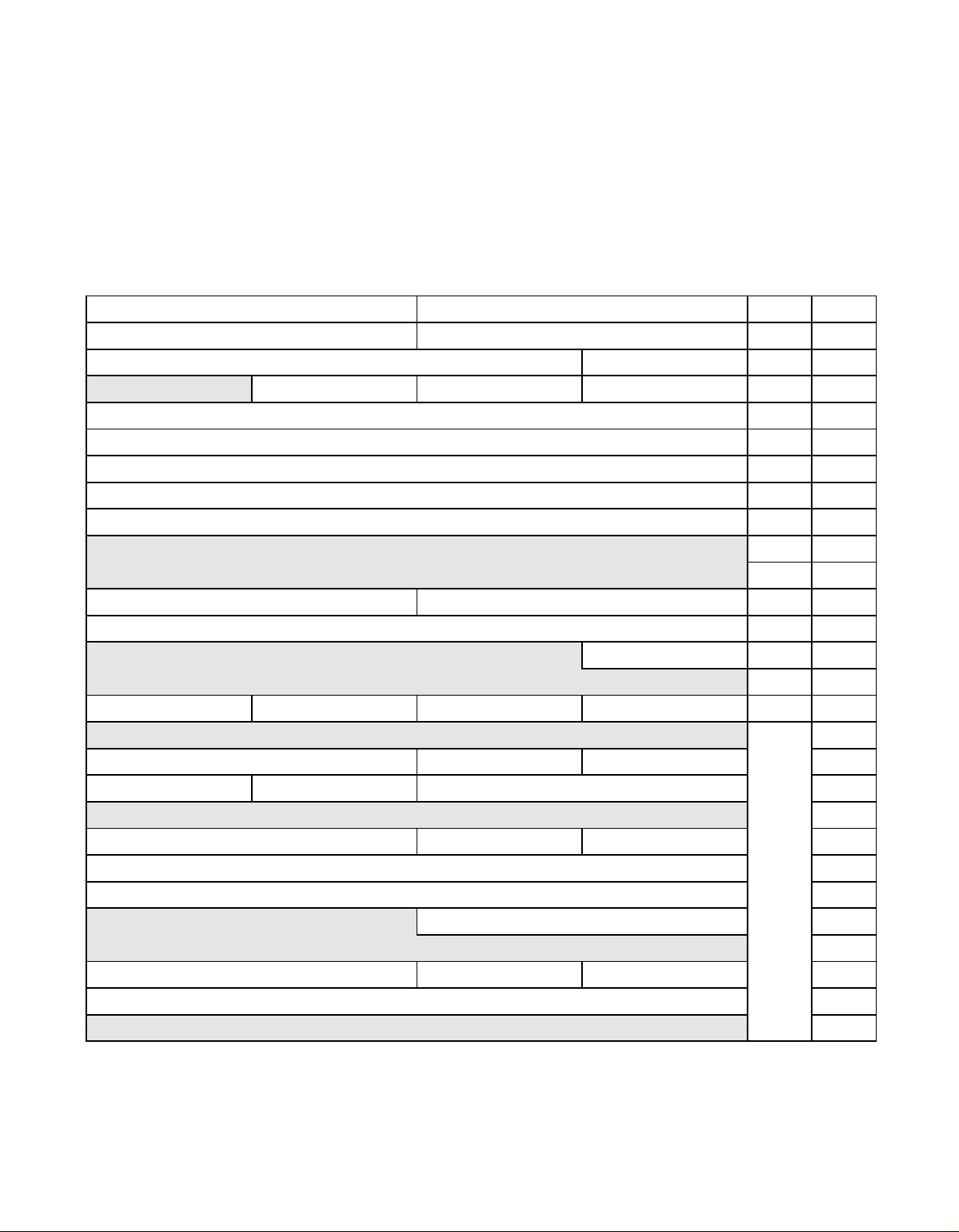
extended capability structures. The address and location of the PCI
extended capability structures are subject to change. To access a PCI
extended capability structure, follow the pointers held in the Capability
Pointer registers and identify the extended capability structure with the
Capability ID register for the given structure.
Table 4.1 LSI53C1020 PCI Configuration Space Address Map
31 24 23 16 15 8 7 0 Offset Page
Device ID Vendor ID 0x00 4-3
Status Command 0x04 4-3
Class Code Revision ID 0x08 4-7
Reserved Header Type Latency Timer Cache Line Size 0x0C 4-8
I/O Base Address 0x10 4-9
Memory [0] Low 0x14 4-10
Memory [0] High 0x18 4-10
Memory [1] Low 0x1C 4-11
Memory [1] High 0x20 4-11
Reserved
Subsystem ID Subsystem Vendor ID 0x2C 4-13
Expansion ROM Base Address 0x30 4-15
Capabilities Pointer 0x34 4-16
Reserved
Maximum Latency Minimum Grant Interrupt Pin Interrupt Line 0x3C 4-17
Reserved
Power Management Capabilities PM Next Pointer PM Capability ID 4-19
PM Data PM BSE Power Management Control/Status 4-21
Reserved –
Message Control MSI Next Pointer MSI Capability ID 4-23
Message Address 4-25
Message Upper Address 4-25
Message Data 4-26
Reserved –
PCI-X Command PCI-X Next Pointer PCI-X Capability ID 4-27
PCI-X Status 4-29
Reserved –
0x24 –
0x28 –
0x38 –
0x40–
0x7F
–
4-2 PCI Host Register Description
Version 2.4 Copyright © 2001–2004 by LSI Logic Corporation. All rights reserved.
Page 81

Register: 0x00–0x01
Vendor ID
Read Only
15 0
Vendor ID
0001000000000000
Vendor ID [15:0]
This 16-bit register identifies the manufacturer of the
device. The Vendor ID is 0x1000.
Register: 0x02–0x03
Device ID
Read Only
15 0
Device ID
0000000000110000
Device ID [15:0]
This 16-bit register identifies the particular device. The
default Device ID is 0x0030.
Register: 0x04–0x05
Command
Read/Write
15 109876543210
Command
0 0 0 0 000000000000
The Command register provides coarse control over the PCI function’s
ability to generate and respond to PCI cycles. Writing a zero to this
register logically disconnects the LSI53C1020 PCI function from the PCI
bus for all accesses except configuration accesses.
PCI Configuration Space Register Descriptions 4-3
Version 2.4 Copyright © 2001–2004 by LSI Logic Corporation. All rights reserved.
Page 82

Reserved [15:11]
This field is reserved.
Interrupt Disable 10
Setting this bit disables the LSI53C1020A from asserting
the interrupt signal. Clearing this bit enablesthe assertion
of its interrupt signal. This bit’s state after RST/ is 0.
(Interrupt Disable is supported only by the LSI53C1020A
controller.)
Reserved 9
This bit is reserved.
SERR/ Enable 8
Setting this bit enables the LSI53C1020 to activate the
SERR/ driver. Clearing this bit disables the SERR/ driver.
Reserved 7
This bit is reserved.
Enable Parity Error Response 6
Setting this bit enables the LSI53C1020 PCI function to
detect parity errors on the PCI bus and report these
errors to the system. Clearing this bit causes the
LSI53C1020 PCI function to set the Detected Parity Error
bit, bit 15 in the PCI Status register, but not to assert
PERR/ when the PCI function detects a parity error. This
bit only affects parity checking. The PCI function always
generates parity for the PCI bus.
Reserved 5
This bit is reserved.
Write and Invalidate Enable 4
Setting this bit enables the PCI function to generate write
and invalidate commands on the PCI bus when operating
in the conventional PCI mode.
Reserved 3
This bit is reserved.
Enable Bus Mastering 2
Setting this bit allows the PCI function to behave as a PCI
bus master. Clearing this bit disables the PCI function
from generating PCI bus master accesses.
4-4 PCI Host Register Description
Version 2.4 Copyright © 2001–2004 by LSI Logic Corporation. All rights reserved.
Page 83

Enable Memory Space 1
This bit controls the ability of the PCI function to respond
to Memory Space accesses. Setting this bit allows the
LSI53C1020 to respond to Memory Space accesses at
the address range specified by the Memory [0] Low,
Memory [0] High, Memory [1] Low, Memory [1] High, and
Expansion ROM Base Address registers. Clearing this bit
disables the PCI function’s response to Memory Space
accesses.
Enable I/O Space 0
This bit controls the PCI function’s response to I/O Space
accesses. Setting this bit enables the PCI function to
respond to I/O Space accesses at the address range the
PCI Configuration Space I/O Base Address register specifies. Clearing this bit disables the PCI function’s
response to I/O Space accesses.
Register: 0x06–0x07
Status
Read/Write
15141312111098765432 0
Status
000000100 01100 0 0
Reads to this 16-bit register behave normally. To clear a bit location that
is currently set, write the bit to one (1). For example, to clear bit 15 when
it is set, without affecting any other bits, write 0x8000 to the register.
Detected Parity Error (from Slave) 15
This bit is set according to the PCI Local Bus Specification, Revision 2.2, and PCI-X Addendum to the PCI Local
Bus Specification, Revision 1.0a.
Signaled System Error 14
The LSI53C1020 PCI function sets this bit when asserting the SERR/ signal.
Received Master Abort (from Master) 13
A master device sets this bit when a Master Abort command terminates its transaction (except for Special
Cycle).
PCI Configuration Space Register Descriptions 4-5
Version 2.4 Copyright © 2001–2004 by LSI Logic Corporation. All rights reserved.
Page 84

Received Target Abort (from Master) 12
A master device sets this bit when a Target Abort command terminates its transaction.
Reserved 11
This bit is reserved.
DEVSEL/ Timing [10:9]
These two read-only bits encode the timing of DEVSEL/
and indicate the slowest time that a device asserts
DEVSEL/ for any bus command except Configuration
Read and Configuration Write. The LSI53C1020 only
supports medium DEVSEL/ timing. The possible timing
values are as follows:
0b00 Fast
0b01 Medium
0b10 Slow
0b11 Reserved
Data Parity Error Reported 8
This bit is set according to the PCI Local Bus Specification, Revision 2.2, and PCI-X Addendum to the PCI Local
Bus Specification, Revision 1.0a. Refer to bit 0 of the
PCI-X Command register for more information.
Reserved [7:6]
This field is reserved.
66 MHz Capable 5
The MAD[13] Power-On Sense pin controls this bit.
Allowing the internal pull-down to pull MAD[13] LOW sets
this bit and indicates to the host system that the
LSI53C1020 PCI function is capable of operating at
66 MHz. Pulling MAD[13] HIGH clears this bit and indicates to the host system that the LSI53C1020 PCI function is not configured to operate at 66 MHz. Refer to
Section 3.10, “Power-On Sense Pins Description,”
page 3-18, for more information.
New Capabilities 4
The LSI53C1020 PCI function sets this read-only bit to
indicate a list of PCI extended capabilities such as PCI
Power Management, MSI, and PCI-X support.
4-6 PCI Host Register Description
Version 2.4 Copyright © 2001–2004 by LSI Logic Corporation. All rights reserved.
Page 85

Interrupt Status 3
This read-only bit reflects the state of the interrupt in the
LSI53C1020A. The interrupt signal is asserted only when
the Interrupt Disable bit in the command register is
cleared and this Interrupt Status bit is set. (Interrupt Status is supported only by the LSI53C1020A controller.)
Reserved [2:0]
This field is reserved.
Register: 0x08
Revision ID
Read/Write
7 0
Revision ID
XXXXXXXX
Revision ID [7:0]
This 8-bit register indicates the current revision level of
the device.
Register: 0x09–0x0B
Class Code
Read Only
23 0
Class Code
000000010000000000000000
Class Code [23:0]
This 24-bit register identifies the generic function of the
device. The upper byte of this register is a base class
code, the middle byte is a subclass code, and the lower
byte identifies a specific register-level programming interface. The value of this register is 0x010000, which identifies a SCSI controller.
PCI Configuration Space Register Descriptions 4-7
Version 2.4 Copyright © 2001–2004 by LSI Logic Corporation. All rights reserved.
Page 86

Register: 0x0C
Cache Line Size
Read/Write
7320
Cache Line Size
00000
Cache Line Size [7:3]
This 8-bit register specifies the system cache line size in
units of 32-bit words. In the conventional PCI mode, the
LSI53C1020 PCI function uses this register to determine
whether to use Write and Invalidate or Write commands
for performing write cycles. Programming this register to
a number other than a nonzero power of two disables the
the use of the PCI performance commands to execute
data transfers. The PCI function ignores this register
when operating in the PCI-X mode.
Reserved [2:0]
This field is reserved.
Register: 0x0D
Latency Timer
Read/Write
0 0 0
7430
0X000 0 0 0
Latency Timer [7:4]
This 8-bit register specifies, in units of PCI bus clocks, the
value of the Latency Timer for this PCI bus master. If the
LSI53C1020 initializes in the PCI mode, the default value
of this register is 0x00. If the LSI53C1020 initializes in the
PCI-X mode, the default value of this register is 0x40.
Reserved [3:0]
This field is reserved.
4-8 PCI Host Register Description
Version 2.4 Copyright © 2001–2004 by LSI Logic Corporation. All rights reserved.
Latency Timer
Page 87
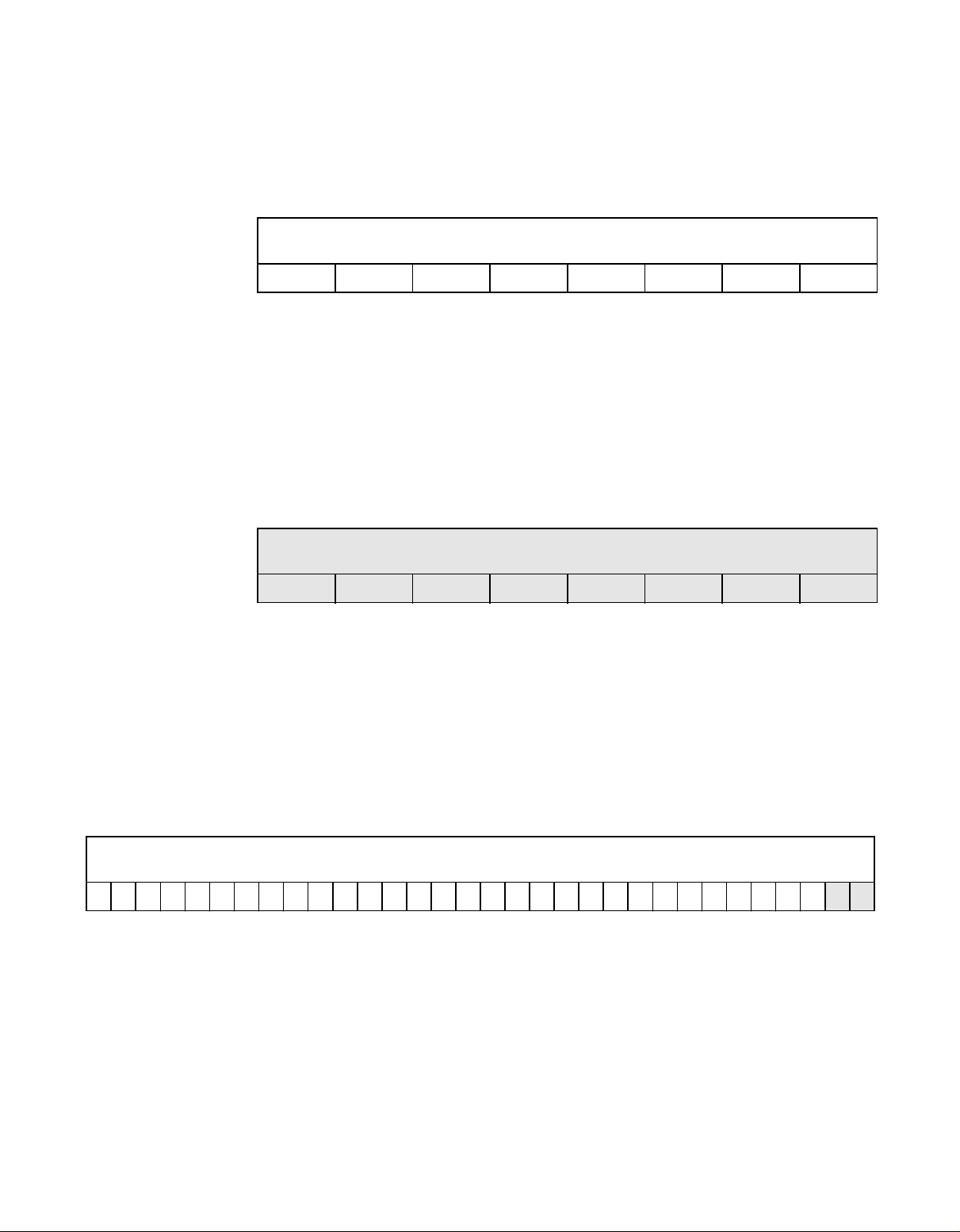
Register: 0x0E
Header Type
Read Only
7 0
Header Type
00000000
Header Type [7:0]
This 8-bit register identifies the layout of bytes 0x10
through 0x3F in configuration space and identifies the
LSI53C1020 as a single function PCI device.
Register: 0x0F
Reserved
7 0
Reserved
0 0 0 0 0 0 0 0
Reserved [7:0]
This register is reserved.
Register: 0x10–0x13
I/O Base Address
Read/Write
31 210
I/O Base Address
0000000000000000000000000000000 1
The I/O Base Address register maps the operating register set into
I/O Space. The LSI53C1020 requires 256 bytes of I/O Space for this
base address register. Hardware sets bit 0 to 0b1. Bit 1 is reserved and
returns 0b0 on all reads.
I/O Base Address [31:2]
This field contains the I/O Base address.
PCI Configuration Space Register Descriptions 4-9
Version 2.4 Copyright © 2001–2004 by LSI Logic Corporation. All rights reserved.
Page 88

Reserved [1:0]
This field is reserved.
Register: 0x14–0x17
Memory [0] Low
Read/Write
31 0
Memory [0] Low
0000000000000000000000 0 0 0 0 0 0 0 1 0 0
The Memory [0] Low register and the Memory [0] High register map
SCSI operating registers into Memory Space [0]. This register contains
the lower 32 bits of the Memory Space [0] base address. Hardware
programs bits [9:0] to 0b0000000100, which indicates that the Memory
Space [0] base address is 64 bits wide and that the memory data is not
prefetchable. The LSI53C1020 requires 1024 bytes of memory space.
Memory [0] Low [31:0]
This field contains the Memory [0] Low address.
Register: 0x18–0x1B
Memory [0] High
Read/Write
31 0
Memory [0] High
00000000000000000000000000000000
The Memory [0] High register and the Memory [0] Low register map
SCSI operating registers into Memory Space [0]. This register contains
the upper 32 bits of the Memory Space [0] base address. The
LSI53C1020 requires 1024 bytes of memory space.
Memory [0] High [31:0]
This field contains the Memory [0] High address.
4-10 PCI Host Register Description
Version 2.4 Copyright © 2001–2004 by LSI Logic Corporation. All rights reserved.
Page 89

Register: 0x1C–0x1F
Memory [1] Low
Read/Write
31 0
Memory [1] Low
000000000000000000
0 0 0 0 0 0 0 0 0 0 0 1 0 0
The Memory [1] Low register and the Memory [1] High register map the
RAM into Memory Space [1]. This register contains the lower 32 bits of
the Memory Space [1] base address. Hardware programs bits [12:0] to
0b0000000000100, which indicates that the Memory Space [1] base
address is 64 bits wide and that the memory data is not prefetchable.
The LSI53C1020 requires 64 Kbytes of memory for Memory Space [1].
Memory [1] Low [31:0]
This field contains the Memory [1] Low address.
Register: 0x20–0x23
Memory [1] High
Read/Write
31 0
Memory [1] High
00000000000000000000000000000000
The Memory [1] High register and the Memory [1] Low register map the
RAM into Memory Space [1]. This register contains the upper 32 bits of
the Memory Space [1] base address. The LSI53C1020 requires
64 Kbytes of memory for Memory Space [1].
Memory [1] High [31:0]
This field contains the Memory [1] High address.
PCI Configuration Space Register Descriptions 4-11
Version 2.4 Copyright © 2001–2004 by LSI Logic Corporation. All rights reserved.
Page 90

Register: 0x24–0x27
Reserved
31 0
Reserved
0 0 0 0 0 0 0 0 0 0 0 0 0 0 0 0 0 0 0 0 0 0 0 0 0 0 0 0 0 0 0 0
Reserved [31:0]
This register is reserved.
Register: 0x28–0x2B
Reserved
31 0
Reserved
0 0 0 0 0 0 0 0 0 0 0 0 0 0 0 0 0 0 0 0 0 0 0 0 0 0 0 0 0 0 0 0
Reserved [31:0]
This register is reserved.
4-12 PCI Host Register Description
Version 2.4 Copyright © 2001–2004 by LSI Logic Corporation. All rights reserved.
Page 91

Register: 0x2C–0x2D
Subsystem Vendor ID
Read Only
15 0
Subsystem Vendor ID
xxxxxxxxxxxxxxxx
Subsystem Vendor ID [15:0]
This 16-bit register uniquely identifies the vendor that
manufactures the add-in board or subsystem where the
LSI53C1020 resides. This register provides a mechanism
for an add-in card vendor to distinguish their cards from
another vendor’s cards, even if the cards use the same
PCI controller (and have the same Vendor ID and
Device ID).
The external serial EEPROM can hold a vendor-specific,
16-bit value for this register, which the board designer
must obtain from the PCI Special Interest Group
(PCI-SIG). By default, an internal pull-down on the
MAD[7] Power-On Sense pin enables the serial EEPROM
interface so that the LSI53C1020 can load this register
from the serial EEPROM at power-up. If the download
from the EEPROM fails, this register contains 0x0000.
If the board designer disables the EEPROM interface by
pulling the MAD[7] Power-On Sense pin HIGH, this register returns a value of 0x1000. Refer to Section 3.10,
“Power-On Sense Pins Description,” page 3-18, for more
information.
PCI Configuration Space Register Descriptions 4-13
Version 2.4 Copyright © 2001–2004 by LSI Logic Corporation. All rights reserved.
Page 92

Register: 0x2E–0x2F
Subsystem ID
Read Only
15 0
Subsystem ID
xxxxxxxxxxxxxxxx
Subsystem ID [15:0]
This 16-bit register uniquely identifies the add-in board or
subsystem where this PCI device resides. This register
provides a mechanism for an add-in card vendor to distinguish their cards from one another even if the cards
use the same PCI controller (and have the same
Vendor ID and Device ID). The board designer can store
a vendor-specific, 16-bit value in an external serial
EEPROM.
The ID Control Power-On Sense pin (MAD[10]) and the
serial EEPROM enable Power-On Sense pin (MAD[7])
control the value of this register. These pins have internal
pull-downs. Allowing MAD[7] to remain internally pulled
down enables the serial EEPROM interface and permits
the LSI53C1020 to load this register from the serial
EEPROM at power up. Pulling MAD[7] HIGH disables the
serial EEPROM interface. Allowing the ID Control pin to
remain internally pulled LOW has no effect on this register. Pulling the ID Control pin HIGH sets bit [15] of this
register. Pulling the ID Control pin HIGH takes precedence over all other settings for bit [15].
Table 4.2 lists the configuration options for the Power-On
Sense pins and settings for this register. If the serial
EEPROM interface is disabled and the ID Control pin is
internally pulled LOW, this register contains 0x1000. If the
serial EEPROM interface is disabled and the ID Control
pin is pulled HIGH, this register contains 0x8000. If a
download from the serial EEPROM fails and the
ID Control pin is internally pulled LOW, this register contains 0x0000. If a download from the serial EEPROM fails
and the ID Control pin is pulled HIGH, this register contains 0x8000. Refer to Section 3.10, “Power-On Sense
Pins Description,” page 3-18, for additional information.
4-14 PCI Host Register Description
Version 2.4 Copyright © 2001–2004 by LSI Logic Corporation. All rights reserved.
Page 93

Table 4.2 Subsystem ID Register Download Conditions and Values
MAD[7] State MAD[10] LOW MAD[10] HIGH
MAD[7] LOW
MAD[7] HIGH
1. The Subsystem ID register returns 0x0000 if the serial EEPROM download fails.
2. The Subsystem ID register returns 0x8000 if the serial EEPROM download fails.
Subsystem ID = 0xXXXX
Bits [15:0] are downloaded.
Subsystem ID register = 0x1000. Subsystem ID = 0x8000.
1
(Default)
Subsystem ID = 0b1XXXXXXXXXXXXXXX
Bits [14:0] are downloaded with Bit [15] set.
Register: 0x30–0x33
Expansion ROM Base Address
Read/Write
31 11 10 1 0
Expansion ROM Base Address
000000000000000000000
This four-byte register contains the base address and size information for
the expansion ROM.
Expansion ROM Base Address [31:11]
These bits correspond to the upper 21 bits of the expansion ROM base address. The host system detects the
size of the external memory by first writing 0xFFFFFFFF
to this register and then reading the register back. The
LSI53C1020 responds with zeros in all don’t care locations. The least significant one (1) that remains represents the binary version of the external memory size. For
example, to indicate an external memory size of 32
Kbytes, this register returns ones in the upper 17 bits
when written with 0xFFFFFFFF and read back.
0 0 0 0 0 0 0 0 0 00
2
Reserved [10:1]
This field is reserved.
Expansion ROM Enable 0
This bit controls if the device accepts accesses to its
expansion ROM. Setting this bit enables address decoding. Depending on the system configuration, the device
can optionally use an expansion ROM. Note that to
PCI Configuration Space Register Descriptions 4-15
Version 2.4 Copyright © 2001–2004 by LSI Logic Corporation. All rights reserved.
Page 94

access the expansion ROM, the user must also set bit 1
in the PCI Command register.
Register: 0x34
Capabilities Pointer
Read Only
7 0
Capabilities Pointer
XXXXXXXX
Capabilities Pointer [7:0]
This 8-bit register indicates the location of the first
extended capabilities register in PCI Configuration
Space. The value of this register varies according to system configuration.
Register: 0x35–0x37
Reserved
23 0
Reserved
0 0 0 0 0 0 0 0 0 0 0 0 0 0 0 0 0 0 0 0 0 0 0 0
Reserved [23:0]
This register is reserved.
Register: 0x38–0x3B
Reserved
31 0
Reserved
0 0 0 0 0 0 0 0 0 0 0 0 0 0 0 0 0 0 0 0 0 0 0 0 0 0 0 0 0 0 0 0
Reserved [31:0]
This register is reserved.
4-16 PCI Host Register Description
Version 2.4 Copyright © 2001–2004 by LSI Logic Corporation. All rights reserved.
Page 95

Register: 0x3C
Interrupt Line
Read/Write
7 0
Interrupt Line
00000000
Interrupt Line [7:0]
This 8-bit register communicates interrupt line routing
information. Power-On-Self-Test (POST) software writes
the routing information into this register as it configures
the system. This register indicates the system interrupt
controller input to which the PCI function’s interrupt pin
connects. System architecture determines the values in
this register.
Register: 0x3D
Interrupt Pin
Read Only
7 0
Interrupt Pin
00000001
Interrupt Pin [7:0]
The encoding of this read-only register indicates which
interrupt pin the function uses. The value for the PCI
function is 0x01, which indicates that the PCI function
presents interrupts on the INTA/ or ALT_INTA pins. The
Interrupt Request Routing Mode bits, bits [9:8] in the Host
Interrupt Mask register, determine if the function presents
interrupts on INTA/, ALT_INTA, or both.
PCI Configuration Space Register Descriptions 4-17
Version 2.4 Copyright © 2001–2004 by LSI Logic Corporation. All rights reserved.
Page 96

Register: 0x3E
Minimum Grant
Read Only
7 0
Minimum Grant
00010000
Min_Gnt [7:0]
This 8-bit register specifies the desired settings for the
latency timer values in units of 0.25 µs. This register
specifies how long of a burst period the device needs.
The LSI53C1020 sets this register to 0x10, indicating a
burst period of 4.0 µs.
Register: 0x3F
Maximum Latency
Read Only
7 0
Maximum Latency
00000110
Max_Lat [7:0]
This 8-bit register specifies the desired settings for the
latency timer values in units of 0.25 µs. This register
specifies how often the device needs to gain access to
the PCI bus. The LSI53C1020 SCSI function sets this
register to 0x06 because it requires the PCI bus every
1.5 µs to maintain a data transfer rate of 320 Mbytes/s.
4-18 PCI Host Register Description
Version 2.4 Copyright © 2001–2004 by LSI Logic Corporation. All rights reserved.
Page 97

Register: 0xXX
Power Management Capability ID
Read Only
7 0
Power Management Capability ID
00000001
Power Management Capability ID [7:0]
This 8-bit register indicates the type of the current data
structure. This register is set to 0x01 to indicate the
Power Management Data Structure.
Register: 0xXX
Power Management Next Pointer
Read Only
7 0
Power Management Next Pointer
XXXXXXXX
Power Management Next Pointer [7:0]
This 8-bit register contains the pointer to the next item in
the PCI function’s extended capabilities list. The value of
this register varies according to system configuration.
PCI Configuration Space Register Descriptions 4-19
Version 2.4 Copyright © 2001–2004 by LSI Logic Corporation. All rights reserved.
Page 98

Register: 0xXX
Power Management Capabilities
Read Only
15 11 10 9 8 6 5 4 3 2 0
Power Management Capabilities
0 0 0 0 0 11000000010
PME_Support [15:11]
These bits define the power management states in which
the device asserts the Power Management Event (PME)
pin. The LSI53C1020 clears these bits because the
LSI53C1020 does not provide a PME signal.
D2_Support 10
The PCI function sets this bit because the LSI53C1020
supports power management state D2.
D1_Support 9
The PCI function sets this bit because the LSI53C1020
supports power management state D1.
Aux_Current [8:6]
The PCI function clears this field because the
LSI53C1020 does not support Aux_Current.
Device Specific Initialization 5
The PCI function clears this bit because no special initialization is required before a generic class device driver
can use it.
Reserved 4
This bit is reserved.
PME Clock 3
The LSI53C1020 clears this bit because the chip does
not provide a PME pin.
Version [2:0]
The PCI function programs these bits to 0b010 to indicate
that the LSI53C1020 complies with the PCI Power Man-
agement Interface Specification, Revision 1.1.
4-20 PCI Host Register Description
Version 2.4 Copyright © 2001–2004 by LSI Logic Corporation. All rights reserved.
Page 99

Register: 0xXX
Power Management Control/Status
Read/Write
15 14 13 12 9 8 7 2 1 0
Power Management Control/Status
00000000
PME_Status 15
The PCI function clears this bit because the LSI53C1020
does not support PME signal generation from D3
Data_Scale [14:13]
The PCI function clears these bits because the
LSI53C1020 does not support the Power Management
Data register.
Data_Select [12:9]
The PCI function clears these bits because the
LSI53C1020 does not support the Power Management
Data register.
PME_Enable 8
The PCI function clears this bit because the LSI53C1020
does not provide a PME signal and disables PME assertion.
Reserved [7:2]
This field is reserved.
0 0 0 0 0 000
.
cold
Power State [1:0]
These bits determine the current power state of the
LSI53C1020. Power states are as follows:
0b00 D0
0b01 D1
0b10 D2
0b11 D3
PCI Configuration Space Register Descriptions 4-21
Version 2.4 Copyright © 2001–2004 by LSI Logic Corporation. All rights reserved.
hot
Page 100

Register: 0xXX
Power Management Bridge Support Extensions
Read Only
7 0
Power Management Bridge Support Extensions
00000000
Power Management Bridge Support Extensions [7:0]
This 8-bit register indicates PCI Bridge specific functionality. The LSI53C1020 always returns 0x00 in this register.
Register: 0xXX
Power Management Data
Read Only
7 0
Power Management Data
00000000
Power Management Data [7:0]
This 8-bit register provides an optional mechanism for the
function to report state-dependent operating data. The
LSI53C1020 always returns 0x00 in this register.
Register: 0xXX
MSI Capability ID
Read Only
7 0
MSI Capability ID
00000101
MSI Capability ID [7:0]
This 8-bit register indicates the type of the current data
structure. This register always returns 0x05, indicating
Message Signaled Interrupts (MSIs).
4-22 PCI Host Register Description
Version 2.4 Copyright © 2001–2004 by LSI Logic Corporation. All rights reserved.
 Loading...