

Page 1

PROGRAMMING
GUIDE
SCSI SCRIPTS™
Processors
Version 2.3
October 2000
®
S14044.A
Page 2

This document contains proprietary information of LSI Logic Corporation. The
information contained herein is not to be used by or disclosed to third parties
without the express written permission of an officer of LSI Logic Corporation.
LSI Logic products are not intended for use in life-support appliances, devices,
or systems. Use of any LSI Logic product in such applications without written
consent of the appropriate LSI Logic officer is prohibited.
DB15-000159-01, Second Edition (October 2000)
This document describes the LSI Logic Corporation SCSI SCRIPTS
™
Processors and will remain the official reference source for all revisions/releases
of this product until rescinded by an update.
To receive product literature, visit us at http://www.lsilogic.com.
LSI Logic Corporation reserves the right to make changes to any products herein
at any time without notice. LSI Logic does not assume any responsibility or
liability arising out of the application or use of any product described herein,
except as expressly agreed to in writing by LSI Logic; nor does the purchase or
use of a product from LSI Logic convey a license under any patent rights,
copyrights, trademark rights, or any other of the intellectual property rights of
LSI Logic or third parties.
Copyright © 1995–2000 by LSI Logic Corporation. All rights reserved.
Ultra SCSI is the term used by the SCSI Trade Association (STA) to describe
Fast-20 SCSI, as documented in the SCSI-3 Fast-20 Parallel Interface standard,
X3.277-199X.
Ultra2 SCSI is the term used by the SCSI Trade Association (STA) to describe
Fast-40 SCSI, as documented in the SCSI Parallel Interface-2 standard, (SPI-2)
X3710-1142D.
TRADEMARK ACKNOWLEDGMENT
The LSI Logic logo design, NASM, SCRIPTS, LVD Link, and TolerANT are
trademarks or registered trademarks of LSI Logic Corporation. All other brand
and product names may be trademarks of their respective companies.
ii
Page 3

Audience
Preface
This book is the primary reference and programming guide for the
LSI Logic PCI to SCSI I/O Processors. It contains a complete functional
description for the LSI Logic PCI to SCSI I/O Processors and includes
complete physical and electrical specifications for the LSI Logic PCI to
SCSI I/O Processors.
This manual is written for users who are familiar with the SCSI and PCI
specifications, and have a working knowledge of computer architectures
and programming. It is specifically designed for use with programming
the LSI Logic SCSI SCRIPTS™ processor in the following chip families:
• LSI53C7XX
Organization
• LSI53C8XX
• LSI53C10XX (up to the LSI53C1010 and LSI53C1010R)
This document has the following chapters and appendixes:
• Chapter 1, Using the Programming Guide, introduces the
SCRIPTS processor features and functions, and the parts of the PCI
to SCSI system that are involved in operating the chip.
• Chapter 2, Programming with SCRIPTS, describes the SCRIPTS
processor and programming language in depth, including how
SCRIPTS programs are integrated with “C” code to execute SCSI
commands.
• Chapter 3, The SCSI SCRIPTS Processor Instruction Set,
describes the SCRIPTS processor instruction set, along with detailed
Preface iii
Page 4

functional descriptions and usage guidelines for all of the instructions
supported.
• Chapter 4, Using the LSI Logic Assembler NASM™, describes
use and operation of the LSI Logic Assembler (NASM).
• Chapter 5, The NASM Output File, describes the LSI Logic
Assembler (NASM) output file.
• Chapter 6, Using the Registers to Control Chip Operations,
contains functional and address information on the
LSI53C7XX/8XX/10XX family chips register set.
• Chapter 7, Integrating SCRIPTS Programs into “C” Language
Drivers, illustrates the relationship between the SCRIPTS program
and the “C” language device driver.
• Chapter 8, Writing Device Drivers with SCRIPTS, addresses
specific kinds of driver applications, with code samples for all
applications discussed.
• Chapter 9, SCRIPTS Programming Topics, addresses specific
kinds of driver applications, with code samples for all applications
discussed.
• Chapter 10, Multithreaded I/O, contains guidelines for writing
SCRIPTS for multithreaded applications.
• Chapter 11, Using the SCRIPTS Processor in Target
Applications, provides guidelines that are specific to using the
SCRIPTS processor in a target device.
• Chapter 12, Debugging the SCRIPTS Processor, provides
information on debugging SCRIPTS programs.
• Chapter 13, New SCRIPTS Processor Features,provides
information on the new 64-bit features of the latest version of this
chip family.
• Appendix A, NASM Error Messages,providesalistofNASMerror
messages.
• Appendix B, Multithreaded SCRIPTS Example,providesexample
SCRIPTS code.
• Appendix C, Glossary of Terms and Abbreviations, provides
definitions of terms and abbreviations.
iv Preface
Page 5

Related Publications
LSI53C770 SCSI I/O Processor with Ultra SCSI Data Manual,
Version 2.0, LSI Logic Corporation, Order Number T18962I
LSI53C810A PCI-SCSI I/O Processor Data Manual, Version 2.0,
LSI Logic Corporation, Order Number T07962I
LSI53C815 PCI-SCSI I/O Processor with Local ROM Interface
Data Manual, Version 2.0, LSI Logic Corporation, Order Number T10962I
LSI53C825A/825AE PCI-SCSI I/O Processor Data Manual, Version 3.0,
LSI Logic Corporation, Order Number T40937I
LSI53C860 PCI-Ultra SCSI I/O Processor Data Manual, Version 2.0,
LSI Logic Corporation, Order Number T09962I
LSI53C875/875E PCI-Ultra SCSI I/O Processor Data Manual,
Version 4.0, LSI Logic Corporation, Order Number T42984I
LSI53C895 PCI to Ultra2 SCSI I/O Processor with LVD Link™ Universal
Transceivers Technical Manual, Version 3.1, LSI Logic Corporation,
Order Number S14030
LSI53C895A PCI to Ultra2 SCSI Controller Technical Manual,
Version 2.2, LSI Logic Corporation, Order Number S14028.B
LSI53C896 PCI to Dual Channel Ultra2 SCSI Multifunction Controller
Technical Manual, Version 3.1, LSI Logic Corporation,
Order Number S14015.B
LSI53C1000 PCI to Ultra3 SCSI Controller Technical Manual,
Version 2.0, LSI Logic Corporation, Order Number S14050
LSI53C1000R PCI to Ultra160 SCSI Controller Technical Manual,
Version 1.0, LSI Logic Corporation, Order Number S14052
LSI53C1010-33 PCI to Dual Channel Ultra3 SCSI Multifunction
Controller Technical Manual, Version 3.1, LSI Logic Corporation,
Order Number S14025.C
LSI53C1010-66 PCI to Dual Channel Ultra3 SCSI Multifunction
Controller Technical Manual, Version 2.0, LSI Logic Corporation,
Order Number S14049
Preface v
Page 6

LSI53C1010R PCI to Dual Channel Ultra160 SCSI Multifunction
Controller Technical Manual, Version 1.0, LSI Logic Corporation,
Order Number S14053
Conventions Used in This Manual
The following is a list of notational conventions used throughout
this programming guide:
Notation Example Meaning and Use
square braces
[]
courier font
All Caps
Curly braces
{}
{} “...”
|
\
CALL [REL] Addre ss,
[{IF | WHEN} [NOT] CARRY]
program.exe
JUMP [REL] Addre ss,
[{IF | WHEN} [NOT] CARRY]
SELECT [ATN] {FROM Address |
ID}, [REL] Addre ss
SET {ACK|ATN|TAR GET|CARRY }
[and {ACK|ATN|TA RGET|CARR Y}...]
INTFLY int_value ,
[{IF | WHEN} [NOT] CARRY]
RELATIVE baselab el \
Optional items in instruction examples.
Used for code samples, file names,
command line information, prompts,etc.
that appear in body text.
Keywords.
Choosebetweenitems enclosed in curly
braces.
The character enclosed in the curly
braces can be repeated as often as
desired.
OR, select one item from a list.
Line continuation.
vi Preface
Page 7

Revision Record
Revision Date Remarks
2.0 8/96 Initial release.
2.1 6/97 Added chapter on programming multifunction controllers.
2.2 6/00 Miscellaneous updates/format changes.
2.3 10/00 All product names changed from SYM to LSI.
Preface vii
Page 8

viii Preface
Page 9

Contents
Chapter 1 Using the Programming Guide
1.1 Product Overview 1-1
1.2 Benefits of Ultra, Ultra2, and Ultra3 SCSI 1-7
1.3 System Overview 1-8
Chapter 2 Programming with SCRIPTS
2.1 The SCSI SCRIPTS Processor 2-1
2.2 SCRIPTS and the SCSI Bus Phases 2-2
2.3 Assembling SCSI SCRIPTS 2-3
2.4 Using SCSI SCRIPTS 2-6
2.4.1 SCRIPTS Data Sizes 2-6
2.4.2 SCSI SCRIPTS Language Elements 2-6
2.4.3 SCSI SCRIPTS Expressions 2-7
2.4.4 SCSI SCRIPTS Keywords 2-7
2.5 Big and Little Endian Byte Addressing 2-8
2.5.1 SCRIPTS Instruction Sequence 2-8
2.5.2 Operating Register Access from Firmware 2-9
2.5.3 Operating Register Access from SCRIPTS
Routines 2-9
2.5.4 User Data Byte Ordering 2-9
Chapter 3 The SCSI SCRIPTS Processor Instruction Set
3.1 Overview of SCRIPTS Instructions 3-1
3.1.1 I/O Instructions 3-1
3.1.2 Memory Move Instructions 3-2
3.1.3 Transfer Control Instructions 3-2
3.1.4 Read/Write Instructions 3-3
3.1.5 Block Move Instructions 3-3
3.1.6 Load and Store Instructions 3-3
Contents ix
Page 10

3.2 Instruction Descriptions 3-4
3.2.1 CALL 3-5
3.2.2 CHMOV 3-10
3.2.3 CLEAR 3-14
3.2.4 DISCONNECT 3-16
3.2.5 INT 3-17
3.2.6 INTFLY 3-21
3.2.7 JUMP 3-27
3.2.8 JUMP 64 3-32
3.2.9 LOAD 3-37
3.2.10 LOAD64 3-40
3.2.11 MOVE 3-42
3.2.12 MOVE MEMORY 3-46
3.2.13 MOVE REGISTER 3-48
3.2.14 NOP 3-53
3.2.15 RESELECT 3-54
3.2.16 RETURN 3-58
3.2.17 SELECT 3-62
3.2.18 SET 3-64
3.2.19 STORE 3-66
3.2.20 WAIT DISCONNECT 3-68
3.2.21 WAIT SELECT 3-69
3.2.22 WAIT RESELECT 3-71
3.3 Instruction Examples 3-73
3.3.1 I/O Instruction Example 3-74
3.3.2 Memory Move Instruction Example 3-74
3.3.3 Transfer Control Instruction Example 3-76
3.3.4 Read/Write Instruction Example 3-77
3.3.5 Block Move Instruction Example 3-78
3.3.6 Load/Store Instruction Example 3-79
Chapter 4 Using the LSI Logic Assembler NASM™
4.1 Overview 4-1
4.2 Using NASM 4-2
4.3 Command Line Options 4-3
4.3.1 Architecture 4-3
4.3.2 Binary Cross Reference Values 4-4
xContents
Page 11

4.3.3 Error Listing File 4-4
4.3.4 Listing File 4-4
4.3.5 Output File 4-4
4.3.6 Partial “C” Source 4-4
4.3.7 .BIN Output 4-5
4.3.8 Omit Termination Record 4-5
4.3.9 Verbose Messages 4-5
4.3.10 Patch Offsets 4-6
4.4 Example Assembler Command Lines 4-6
4.5 How NASM Parses SCRIPTS Files 4-6
4.6 Assembler Declarative Keywords 4-7
4.6.1 ABSOLUTE 4-8
4.6.2 ARCH 4-8
4.6.3 ENTRY 4-9
4.6.4 EXTERN 4-9
4.6.5 PASS 4-10
4.6.6 PROC 4-10
4.6.7 RELATIVE 4-11
4.6.8 TABLE 4-12
4.7 Conditional Keywords 4-14
4.7.1 IF 4-14
4.7.2 WHEN 4-14
4.8 Logical Keywords 4-14
4.8.1 NOT 4-15
4.8.2 AND 4-15
4.8.3 OR 4-15
4.9 Flag Fields 4-15
4.9.1 ACK 4-15
4.9.2 ATN 4-15
4.9.3 TARGET 4-16
4.9.4 CARRY 4-16
4.10 Qualifier Keywords 4-16
4.10.1 DSAREL 4-16
4.10.2 FROM 4-16
4.10.3 MASK 4-16
4.10.4 MEMORY 4-17
4.10.5 PTR 4-17
4.10.6 REG 4-17
Contents xi
Page 12

4.10.7 REL 4-17
4.10.8 TO 4-17
4.10.9 WITH 4-17
4.10.10 NOFLUSH 4-17
4.11 Other Keywords 4-18
4.11.1 Action Keywords 4-18
4.11.2 SCSI Phases 4-18
4.11.3 Register Names 4-18
Chapter 5 The NASM Output File
5.1 NASM Output Overview 5-1
5.2 NASM Output File Examples 5-2
5.2.1 SCRIPTS Array 5-3
5.2.2 External 5-5
5.2.3 Relative 5-7
5.2.4 Entry 5-9
5.2.5 Label Patches 5-9
5.2.6 Absolute 5-10
5.2.7 Termination Record 5-11
Chapter 6 Using the Registers to Control Chip Operations
6.1 Overview 6-1
6.2 SCSI Registers 6-2
6.3 DMA Registers 6-4
6.4 SCRIPTS Registers 6-5
6.5 64-Bit SCRIPTS Selector Registers 6-6
6.6 Interrupt Registers 6-7
6.7 Phase Mismatch Registers 6-8
6.8 Test and Miscellaneous Registers 6-9
6.9 General Purpose Registers 6-11
6.10 Register Initialization 6-11
Chapter 7 Integrating SCRIPTS Programs into “C” Language Drivers
7.1 Initializing the SCRIPTS Processor 7-1
7.1.1 Reset 7-3
7.1.2 Table Indirect Operations 7-3
7.2 Patching 7-7
xii Contents
Page 13

7.2.1 EXTERN Buffers 7-8
7.2.2 RELATIVE Buffers 7-8
7.2.3 ABSOLUTE Values 7-9
7.2.4 Buffer Addresses 7-9
7.2.5 Byte Counts 7-9
7.2.6 Absolute JUMP/CALL Addresses 7-10
7.2.7 Entry Locations 7-10
7.2.8 Self-Modifying SCRIPTS Code 7-11
7.3 Running a SCRIPTS Program 7-12
Chapter 8 Writing Device Drivers with SCRIPTS
8.1 Device Driver Overview 8-1
8.2 Command Block 8-4
8.3 Power Up Example 8-4
8.4 I/O Request Process 8-5
8.5 How to Write a Device Driver with SCRIPTS 8-6
8.6 Table Indirect Addressing 8-7
8.6.1 Block Move Instructions 8-8
8.6.2 Select/Reselect Instructions 8-9
8.6.3 Defining a Table 8-10
8.7 Relative Addressing 8-11
Chapter 9 SCRIPTS Programming Topics
9.1 Scatter/Gather Operations 9-1
9.2 Loopback Mode 9-4
9.2.1 Loopback Example – Selection 9-5
9.3 Byte Recovery on Target Disconnect 9-9
9.3.1 Saving the Processor State 9-10
9.3.2 Updating the SCRIPTS Program 9-13
9.3.3 Cleaning Up 9-13
9.3.4 Example Byte Recovery Code 9-13
9.4 Synchronous Negotiation and Transf er 9-18
9.5 Interrupt Handling 9-19
9.5.1 Polling and Hardware Interrupts 9-19
9.5.2 Registers 9-20
9.5.3 Fatal vs. Nonfatal Interrupts 9-22
9.5.4 Masking 9-23
Contents xiii
Page 14

9.5.5 Stacked Interrupts 9-24
9.5.6 Halting in an Orderly Fashion 9-24
9.5.7 Sample Interrupt Service Routine 9-25
9.6 Migrating Existing Software to Ultra, Ultra2, and
Ultra3 SCSI 9-26
9.6.1 Clock Divider Bits 9-27
9.6.2 Ultra Enable Bit 9-28
9.6.3 Loading the New Register Values 9-28
9.6.4 Negotiating Synchronous Transfers 9-28
9.6.5 Using the SCSI Clock Doubler 9-29
9.6.6 Using the SCSI Clock Quadrupler 9-29
9.7 Using the SCRIPTS RAM 9-30
9.7.1 Loading SCRIPTS RAM 9-30
9.7.2 Programming Techniques when Using
SCRIPTS RAM 9-31
9.7.3 Patching Internal and External SCRIPTS
Programs 9-37
Chapter 10 Multithreaded I/O
10.1 Overview 10-1
10.2 Multithreaded Operations Flow 10-2
10.3 SCRIPTS Areas 10-4
10.4 Multithreaded SCRIPTS Example 10-4
10.5 Using the SIGP Bit to Abort an Instruction 10-10
10.6 I/O Completion 10-12
Chapter 11 Using the SCRIPTS Processor in Target Applications
11.1 SCSI and Target SCRIPTS Protocol 11-1
11.2 Registers Used for Target Operation 11-3
11.3 Using SCRIPTS for Target Operation 11-3
11.3.1 Sample Target Operation SCRIPTS Program 11-4
11.4 Synchronous Negotiation by a Target Device 11-16
Chapter 12 Debugging the SCRIPTS Processor
12.1 Chip Debugging Guidelines 12-1
12.2 Register Used for Debugging 12-3
xiv Contents
Page 15

Chapter 13 New SCRIPTS Processor Features
13.1 Improved FIFO Flushing 13-1
13.2 Larger FIFO 13-2
13.3 New ISTAT Registers 13-2
13.4 New Scratch Registers 13-2
13.5 New Load/Store Feature 13-2
13.6 Phase Mismatch Handling 13-3
13.6.1 Control Bits 13-3
13.6.2 Registers 13-4
13.6.3 SCRIPTS Example 13-5
13.7 64-Bit SCRIPTS Addressing 13-6
13.7.1 Control Bits 13-6
13.7.2 Block Move 13-7
13.7.3 Direct Block Move 13-7
13.7.4 Mode 0 Table Indirect Block Move 13-7
13.7.5 Mode 1 Table Indirect Block Move 13-8
13.7.6 Table Indirect Block Move Summary 13-10
13.7.7 LSI53C1010/LSI53C1010R 13-10
Appendix A NASM Error Messages
Appendix B Multithreaded SCRIPTS Example
Appendix C Glossary of Terms and Abbreviations
Index
Customer Feedback
Figures
1.1 Single Channel Block Diagram 1-6
1.2 Dual Channel Block Diagram 1-6
1.3 Typical SCRIPTS Operation 1-9
2.1 Overview of Assembling SCSI SCRIPTS 2-5
Contents xv
Page 16

3.1 CALL Format 3-6
3.2 Use of the Mask Keyword 3-9
3.3 CHMOV Format 3-11
3.4 CLEAR Format 3-15
3.5 DISCONNECT Format 3-16
3.6 INT Format 3-18
3.7 INTFLY Format 3-23
3.8 JUMP Format 3-28
3.9 JUMP 64 Format 3-34
3.10 LOAD Format 3-38
3.11 MOVE Format 3-43
3.12 MOVE MEMORY Format 3-47
3.13 MOVE REGISTER Format 3-50
3.14 NOP Format 3-54
3.15 RESELECT Format 3-55
3.16 Reselection Instruction 3-57
3.17 RETURN Format 3-59
3.18 SELECT Format 3-63
3.19 SET Format 3-65
3.20 STORE Format 3-67
3.21 WAIT DISCONNECT Format 3-69
3.22 WAIT SELECT Format 3-70
3.23 WAIT RESELECT Format 3-71
3.24 WAIT RESELECT and the SIGP Bit 3-73
3.25 I/O Instruction Type 3-74
3.26 Memory Move Instruction Part 1 3-75
3.27 Memory Move Instruction Part 2 3-76
3.28 Transfer Control Instruction 3-77
3.29 Read/Write Instruction Example 3-78
3.30 Block Move Instruction 3-79
3.31 Load/Store Instruction 3-80
5.1 Sample SCRIPTS Program 5-2
7.1 Accessing I/O Mapped Registers 7-1
7.2 Resetting the SCRIPTS Processor 7-3
7.3 SCRIPTS Table Declaration 7-4
7.4 Creating Table Indirect Entry Offsets 7-4
7.5 Data Structure and Type Definition 7-5
7.6 Data Structure and Type Definition 7-6
xvi Contents
Page 17

7.7 Creating Buffers 7-7
7.8 Self-Modifying Code 7-11
7.9 General.ss SCRIPTS Source File 7-12
7.10 General.out NASM Output File 7-16
8.1 The Role of the SCSI Device Drivers 8-2
8.2 SCSI Device Driver Layers 8-3
8.3 Power Up Examples 8-5
8.4 I/O Operation 8-6
8.5 Table Indirect Addressing 8-10
8.6 Table Definitions 8-11
9.1 Scatter/Gather Operation 9-2
9.2 Alternate Scatter/Gather Operation 9-4
9.3 Loopback Mode 9-6
9.4 Target Operation 9-7
9.5 Byte Transfer 9-8
9.6 Loopback Mode Selection Procedure 9-9
9.7 SCRIPTS Sequence to Move Data 9-14
9.8 Example Function for Handling DATA IN Phase
Mismatch Interrupts 9-15
9.9 Example Function for Handling DATA OUT Phase
Mismatch Interrupts 9-16
9.10 SELECT FROM Example Code 9-19
9.11 Storing Data Structures in SCRIPTS RAM 9-31
9.12 External Script (SCRIPTS.LIS file) 9-33
9.13 External Script (SCRIPTS.OUT file) 9-34
9.14 Internal Script (SCRIPTS.LIS file) 9-34
9.15 Internal SCRIPTS Program (SCRIPTS.OUT file) 9-36
9.16 Patching Routine 9-38
10.1 Multithreaded System Operation 10-2
10.2 Multithreaded SCRIPTS Operational Flow 10-3
10.3 Multithreaded SCRIPTS Example Step 1 10-5
10.4 Multithreaded SCRIPTS Example Step 2 10-6
10.5 Multithreaded SCRIPTS Example Step 3 10-7
10.6 Multithreaded SCRIPTS Example Step 6 10-7
10.7 Multithreaded SCRIPTS Example Step 10 10-9
10.8 Multithreaded SCRIPTS Example Step 11 10-9
10.9 Multithreaded SCRIPTS Example Step 13 10-10
10.10 Sample SIGP Code 10-10
Contents xvii
Page 18

11.1 SCRIPTS Source Code–Comments 11-4
11.2 SCRIPTS Source Code–ABSOLUTE Declarations 11-5
11.3 SCRIPTS Source Code–EXTERN Variables 11-5
11.4 SCRIPTS Source Code–TABLE 11-6
11.5 SCRIPTS Source Code–ENTRY Declarations 11-7
11.6 SCRIPTS Source Code–wait_select Label 11-7
11.7 SCRIPTS Source Code–CDB Functions 11-8
11.8 SCRIPTS Source Code–Message Out Phase 11-8
11.9 SCRIPTS Source Code–Extended Message 11-9
11.10 SCRIPTS Source Code–Synchronous Negotiation 11-9
11.11 SCRIPTS Source Code–Wide Negotiation 11-9
11.12 SCRIPTS Source Code–Return Negotiation 11-9
11.13 SCRIPTS Source Code–Recovery Message 11-10
11.14 SCRIPTS Source Code–Test Unit Ready 11-10
11.15 SCRIPTS Source Code–stopped_busy_tur Command 11-10
11.16 SCRIPTS Source Code–Request Sense 11-11
11.17 SCRIPTS Source Code–Read Label 11-12
11.18 SCRIPTS Source Code–read_disconnect Label 11-12
11.19 SCRIPTS Source Code–read_reconnect Label 11-13
11.20 SCRIPTS Source Code–Write 11-13
11.21 SCRIPTS Source Code–write_disconnect Label 11-13
11.22 SCRIPTS Source Code–write_reconnect Label 11-14
11.23 SCRIPTS Source Code–reserve_unit Label 11-14
11.24 SCRIPTS Source Code–release_unit Command 11-14
11.25 SCRIPTS Source Code–abort Label 11-15
11.26 SCRIPTS Source Code–stopped_busy_wait_select
Command 11-15
13.1 64-Bit Direct Block Move Format 13-7
13.2 Index Mode 1 Table Entry Format 13-9
Tables
1.1 Features and Functions of LSI53C7XX/8XX/10XX
1.2 Features and Functions of LSI53C7XX/8XX/10XX
2.1 SCSI Protocol and SCRIPTS Instructions 2-2
2.2 Data Sizes 2-6
2.3 SCSI SCRIPTS Language Elements 2-6
xviii Contents
Family Chips (part 1) 1-2
Family Chips (part 2) 1-3
Page 19

2.4 Arithmetic Operators 2-7
2.5 Bitwise Operators 2-7
2.6 Big and Little Endian Byte Addressing 2-8
3.1 Opcode Bit Options 3-2
3.2 Read/Write Instructions 3-3
3.3 SCRIPTS Instructions Set 3-4
3.4 SCSI Phase Bit V alues (CALL Format) 3-7
3.5 SCSI Phase Bit Values (CHMO V Format) 3-12
3.6 SCSI Phase Bit Values (INT Format) 3-18
3.7 SCSI Phase Bit Values (INTFLY Format) 3-23
3.8 SCSI Phase Bit Values (JUMP Format) 3-29
3.9 SCSI Phase Bit Values (JUMP 64 Format) 3-35
3.10 Register Address Field Definitions (LOAD Format) 3-39
3.11 LOAD64 Format 3-41
3.12 Register Address Field Definitions (LOAD64 Format) 3-42
3.13 SCSI Phase Bit Values (MOVE Format) 3-44
3.14 SCSI Phase Bit Values (RETURN Format) 3-59
3.15 Low Order Bit Options 3-68
4.1 Keywords 4-7
5.1 Relationship Between Entry and PROC Statements
and Output File 5-5
6.1 SCSI Registers 6-2
6.2 DMA Registers 6-5
6.3 SCRIPTS Registers 6-6
6.4 64-Bit Selector Registers 6-6
6.5 Interrupt Registers 6-7
6.6 Phase Mismatch Registers 6-9
6.7 Test and Miscellaneous Registers 6-10
6.8 General Purpose Registers 6-11
6.9 LSI53C815/810A/860 Startup Bits 6-12
6.10 LSI53C825A/875/876/885/895/895A/896/10XX
Startup Bits 6-14
8.1 Data Structure 8-9
8.2 I/O Data Structure 8-9
11.1 SCSI Protocol and Target SCRIPTS Instructions 11-2
11.2 Register Bits Used for Target Operation 11-3
13.1 ISTAT1 Register 13-2
13.2 Index Mapping 13-8
Contents xix
Page 20

13.3 Table Indirect BMOV Upper 32-Bit Address Locations 13-10
A.1 NASM Error Messages A-1
A.2 Fatal Errors A-13
A.3 Warnings A-14
xx Contents
Page 21

Chapter 1
Using the
Programming Guide
This chapter provides an overview of the LSI Logic SCSI SCRIPTS
processor. It also provides brief descriptions for some of the chips
containing the processor and their features. The chapter contains the
following sections:
• Section 1.1, “Product Overview”, page 1-1
• Section 1.2, “Benefits of Ultra, Ultra2, and Ultra3 SCSI”, page 1-7
• Section 1.3, “System Overview”, page 1-8
1.1 Product Overview
The LSI Logic SCSI SCRIPTS processor is based on the LSI53C7XX
SCSI I/O Processor family architecture, with a host interface to the
Peripheral Component Interconnect (PCI) bus. The SCRIPTS processor
connects to the PCI bus without glue logic.
Several LSI Logic product families contain the SCRIPTS processor.
• LSI53C7XX
• LSI53C8XX
• LSI53C10XX (up to the LSI53C1010 and LSI53C1010R)
Tables 1.1 and 1.2 list currently available chips using the SCRIPTS
processor and their basic specifications. More detailed information is
available in the respective chip technical manuals, listed in Related
Publications on page v.
SCSI SCRIPTS Processors 1-1
Page 22

Table 1.1 Features and Functions of LSI53C7XX/8XX/10XX Family Chips (part 1)
LSI53C770 LSI53C810A LSI53C860 LSI53C815
Maximum Transfer
Rate
DMA FIFO Size
(bytes)
Synchronous
Offset (levels)
SCRIPTS RAM 4 Kbytes None None None 4 Kbytes
Differential SCSI No No No No HVD
Wide SCSI Yes No No No Yes
External Memory
Interface
Instruction Prefetch Yes Yes Yes No Y es
Load/Store
Instructions
20 Mbytes/s
synchronous
(with Wide
SCSI)
96 80 80 64 88 or 536
16 8 8 8 16
No No No Yes Yes
No Yes Y es No Yes
5Mbytes/s
asynchronous
10 Mbytes/s
synchronous
5Mbytes/s
asynchronous
20 Mbytes/s
synchronous
(with Ultra
SCSI)
5Mbytes/s
asynchronous
10 Mbytes/s
synchronous
LSI53C825A
LSI53C825AJ
10 Mbytes/s
asynchronous
20 Mbytes/s
synchronous
Enhanced Move
Register Capability
SCSI Selected As
ID Bits
Number of 32-bit
SCRATCH
Registers
PCI Caching No Yes Yes No Yes
Selectable IRQ
Disable
Big/Little Endian
Support
PCI Data Bus N/A 32-Bit 32-Bit 32-Bit 32-Bit
1-2 Using the Programming Guide
No No No No Yes
No Yes Y es No Yes
12 2 2 10
No Yes Y es No Yes
Big or Little
Endian
Little Endian Little Endian Big or Little
Endian
Big or Little
Endian (except
LSI53C825AJ)
Page 23

Table 1.1 Features and Functions of LSI53C7XX/8XX/10XX Family Chips (part 1) (Cont.)
LSI53C770 LSI53C810A LSI53C860 LSI53C815
PCI Addressing N/A 32-Bit 32-Bit 32-Bit 32-Bit
Package 208 PQFP 100 PQFP 100 PQFP 128 PQFP 160 PQFP
Table 1.2 Features and Functions of LSI53C7XX/8XX/10XX Family Chips (part 2)
LSI53C875
LSI53C875A
LSI53C875J
Maximum
Transfer Rate
DMA FIFO
Size (bytes)
LSI53C875JB
LSI53C875N
10 Mbytes/s
asynchronous
40 Mbytes/s
synchronous
(with Ultra
SCSI)
88 or 536 112 or 816
LSI53C895
LSI53C895A LSI53C896
10 Mbytes/s
asynchronous
80 Mbytes/s
synchronous
(with Ultra2
SCSI)
(LSI53C895)
112 or 944
(LSI53C895A)
10 Mbytes/s
asynchronous
80 Mbytes/s
synchronous
per channel
for
160 Mbytes/s
112 or 944 896 to 920 896 to 920
LSI53C1000
LSI53C1000R
10 Mbytes/s
asynchronous
160 Mbytes/s
synchronous
(with Ultra2
SCSI)
LSI53C825A
LSI53C825AJ
LSI53C1010
LSI53C1010R
10 Mbytes/s
asynchronous
160 Mbytes/s
synchronous
per channel
for
320 Mbytes/s
Synchronous
Offset (levels)
SCRIPTS RAM 4 Kbytes 4 Kbytes
Differential
SCSI
Wide SCSI Yes Yes Yes
External
Memory
Interface
16 31 31 62 62
(LSI53C895)
8Kbytes
(LSI53C895A)
High Voltage
Differential
(HVD)
Yes Yes Yes Yes Y es
Product Overview 1-3
Low Voltage
Differential
(LVD) and HVD
8Kbytes 8Kbytes 8Kbytes
LVD and HVD LVD and HVD LVD and HVD
Dual Channel
Yes Yes
Dual Channel
Page 24

Table 1.2 Features and Functions of LSI53C7XX/8XX/10XX Family Chips (part 2) (Cont.)
LSI53C875
LSI53C875A
LSI53C875J
LSI53C875JB
LSI53C875N
LSI53C895
LSI53C895A LSI53C896
LSI53C1000
LSI53C1000R
LSI53C1010
LSI53C1010R
Instruction
Prefetch
Load/Store
Instructions
Enhanced
Move Register
Capability
SCSI Selected
As ID Bits
Number of
32-bit
SCRATCH
Register
PCI Caching Yes Yes Yes Yes Yes
SelectableIRQ
Disable
Big/Little
Endian Support
PCI Data Bus 32-Bit 32-Bit 64-Bit 64-Bit 64-Bit
Yes Yes Yes Yes Y es
Yes Yes Yes Yes Y es
Yes Yes Yes Yes Y es
Yes Yes Yes Yes Y es
10 10 (LSI53C895)
Yes Yes Yes Yes Y es
Big or Little
Endian (except
LSI53C875J,
LSI53C875JB)
18
(LSI53C895A)
LSI53C895 Big
or Little Endian
LSI53C895A
Little Endian
18 18 18
Little Endian Little Endian Little Endian
PCI Addressing 32-Bit 32-Bit
(LSI53C895)
64-Bit
(LSI53C895A)
Package 160 PQFP,
169 BGA,
208 PQFP
208 PQFP 329 BGA 329 BGA 329 BGA
The LSI Logic SCSI SCRIPTS processors are the first products to
concentrate the functions of an intelligent SCSI adapter board onto a
single chip. These products integrate a high-performance SCSI core, a
PCI bus master DMA core, and the SCSI SCRIPTS processor to meet
1-4 Using the Programming Guide
64-Bit 64-Bit 64-Bit
Page 25

the flexibility requirements of SCSI-3 and future SCSI standards. It
executes multithreaded I/O algorithms with minimum host processor
intervention, reducing the protocol overhead required for SCSI operations
to as little as one interrupt per SCSI I/O. The SCRIPTS language, a high
level instruction set, provides complete programmability of I/O operations
and supports the flexibility needed for multithreaded I/O algorithms.
SCRIPTS provides:
• Phase sequencing without processor intervention
• Automatic bus arbitration
• Data or phase comparison for independent SCSI algorithm decisions
• DMA interface control
All LSI53C7XX/8XX/10XX family chips are also supported by LSI Logic
software for connecting SCSI devices. This includes BIOS support for
LSI Logic SCSI processors and drivers for most types of SCSI
peripherals under the major operating systems. These chips also feature:
• On-chip Single-Ended (SE) drivers
• Synchronous and asynchronous transfer capabilities
• LSI Logic T olerANT
®
driver and receiver technology
• Bus mastering
• Automatic selection/reselection time-outs
• 32-bit memory addressing
• 32-bit data bus
• PCI bursting
Newer chips, including the LSI53C895, LSI53C895A, LSI53C896,
LSI53C1000, LSI53C1010, LSI53C1010R, and LSI53C1000R also have
these features:
• On-chip LVD
• 64-bit memory addressing
• 64-bit data bus
Note:
Product Overview 1-5
For specific information on the features and functions of the
various chips supporting SCRIPTS, refer to their respective
technical manuals. You must have the appropriate technical
Page 26
manual in order to effectively program SCRIPTS for each
chip.
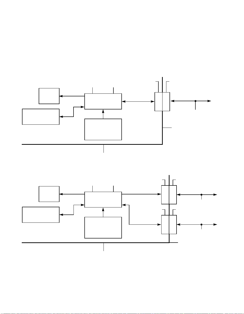
Figures 1.1 and 1.2 are block diagrams of the single and dual channel
LSI Logic chips that support SCRIPTS, with a map of SCSI data and
control paths through the chips.
Figure 1.1 Single Channel Block Diagram
VDD
PCI Bus
Channel Chip
External Memory
(When Supported)
External Oscillator
or Optimal Internal
Connection to
PCI Bus Clock
CPU baseboard
VSS
Single
SCLK
CPU Box
Figure 1 .2 Dual Channel Block Diagram
VDD
PCI Bus
Channel Chip
External Memory
(When Supported)
External Oscillator
or Optimal Internal
Connection to
PCI Bus Clock
CPU baseboard
VSS
Dual
SCLK
SCSI Term ConnectionSCSI Connection
SCSI Bus
Peripheral
Bulkhead
SCSI Term ConnectionSCSI Connection
SCSI Bus
Peripheral
SCSI Term ConnectionSCSI Connection
SCSI Bus
Peripheral
Bulkhead
CPU Box
1-6 Using the Programming Guide
Page 27

1.2 Benefits of Ultra, Ultra2, and Ultra3 SCSI
Ultra SCSI is an extension of the SCSI-3 standard that expands the
bandwidth of the SCSI bus and allows faster synchronous SCSI transfer
rates. When enabled, Ultra SCSI performs 20 megatransfers per second,
which results in approximately doubling the synchronous transfer rates of
Fast SCSI-2. The LSI53C860 and LSI53C875 can perform 8-bit or
16-bit Ultra SCSI synchronous transfers as fast as 20 Mbytes/s or
40 Mbytes/s.
Ultra2 SCSI extends SCSI performance beyond Ultra SCSI rates, up to
40 megatransfers per second. It also defines a new physical interface,
LVD SCSI, that retains the reliability of HVD SCSI while allowing a longer
cable and more devices on the bus than Ultra SCSI. The LSI53C895 can
perform 16-bit, Ultra2 SCSI synchronous transfers as fast as
80 Mbytes/s.
Ultra3 SCSI delivers data up to two times faster than Ultra2 SCSI.
Ultra3 SCSI is an extension of the SPI-3 draft standard. When enabled,
Ultra3 SCSI performs 80 megatransfers per second. Ultra3 data transfer
speed is accomplished using Double Transition (DT) clocking. Data is
clocked on both rising and falling edges of the request and acknowledge
signals, doubling data transfer speeds without increasing the clock rate.
The advantages of Ultra/Ultra2/Ultra3 SCSI are most noticeable in
heavily loaded systems, or large block size applications such as video on
demand and image processing. Not only does it significantly improve
SCSI bandwidth, it also preserves existing hardware and software
investments. LSI Logic Ultra/Ultra2/Ultra3 SCSI chips are all compatible
with Fast SCSI software; the only changes required are to enable the
chip to negotiate for the faster synchronous transfer rates.
Some changes to existing cabling or system designs may be needed to
maintain signal integrity at Ultra SCSI synchronous transfer rates. These
design issues are discussed in the chip technical manuals.
Benefits of Ultra, Ultra2, and Ultra3 SCSI 1-7
Page 28

1.3 System Overview
To execute SCSI SCRIPTS programs, only a SCSI SCRIPTS starting
address is required. All subsequent instructions are fetched from external
memory or internal SCRIPTS RAM (when supported). Depending on the
chip, up to eight Dwords at a time are fetched across the DMA interface
and loaded into the internal chip registers. When the chip is operating at
its highest frequency, instruction fetching and decoding take as little as
500 ns. The chip fetches instructions until a SCRIPTS interrupt occurs or
until an external, unexpected event (such as a hardware error) causes
an interrupt. The full set of SCSI features in the instruction set allows
re-entry to the algorithm at any point. This high level interface can be
used for both normal operation and exception conditions.
A typical SCRIPTS operation is illustrated in Figure 1.3. Before SCRIPTS
operation begins, the host processor writes the Data Structure Address
register value to initialize the pointer for table indirect operations. To
begin SCRIPTS operation, the host processor writes the starting address
of the SCRIPTS instructions into the chip’s DMA SCRIPTS Pointer
Register. Once it receives this address, the chip becomes a bus master
and fetches the first SCRIPTS instruction. The chip executes all steps of
the instruction, moving through the appropriate bus phases, interrupting
only on completion of SCRIPTS operation or when service from the
external processor is required. This leaves the host processor free for
other tasks.
Software developers can create SCSI SCRIPTS source code in any text
editor. The LSI Logic Assembler, NASM, is discussed in Chapter 4,
“Using the LSI Logic Assembler NASM™.” NASM assembles SCRIPTS
code into an array of assembled SCRIPTS instructions that can be
included in the main “C” language program and linked together to create
an executable driver. When compiled, these programs control chip
operation.
1-8 Using the Programming Guide
Page 29
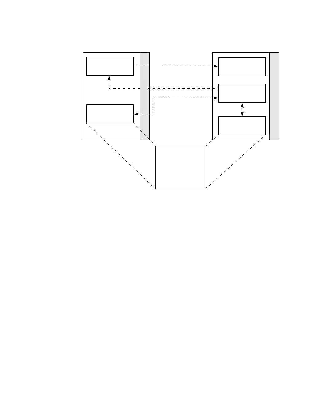
Figure 1.3 Typical SCRIPTS Operation
Host System
Processor
System Memor y
Write DSP
Interrupt when done
Fetch instructions from
internal or external
System Bus
memory
(Expanded View)
Data Structure
Message Buffer
Command Buffer
Data Buffer
Status Buffer
LSI53C7XX/8XX/10XX
Operating
Registers
SCRIPTS
Processor
SCSI Bus
SCRIPTS RAM
(when supported)
System Overview 1-9
Page 30

1-10 Using the Programming Guide
Page 31

Chapter 2
Programming with
SCRIPTS
This chapter contains the following sections:
• Section 2.1, “The SCSI SCRIPTS Processor,” page 2-1
• Section 2.2, “SCRIPTS and the SCSI Bus Phases,” page 2-2
• Section 2.3, “Assembling SCSI SCRIPTS,” page 2-3
• Section 2.4, “Using SCSI SCRIPTS,” page 2-6
• Section 2.5, “Big and Little Endian Byte Addressing,” page 2-8
2.1 The SCSI SCRIPTS Processor
The SCSI SCRIPTS processor permits instructions to be fetched from
internal or external memory. Algorithms written in the SCSI SCRIPTS
language are assembled to control the SCSI and DMA modules.
Complex SCSI bus sequences, including multiple SCRIPTS instructions,
execute independently of the host processor.
The SCSI SCRIPTS reside in host computer memory or internal
SCRIPTS RAM during system operation, allowing for fast execution. If
instructions reside in external memory, the chip fetches SCRIPTS
programs from memory using bus master DMA transfers. If instructions
reside in SCRIPTS RAM, they are fetched directly from RAM without
generating PCI bus traffic. The SCRIPTS processor allows you to fine
tune SCSI operations such as adjusting to new device types, adapting to
changes in SCSI logical definitions, or quickly incorporating new options,
such as vendor unique commands or new SCSI specifications. The
SCRIPTS processor fetches SCRIPTS instructions from system memory
to control chip operation. The SCRIPTS processor does not compile
code; SCRIPTS programs must be assembled for execution by the
NASM assembler and then compiled with a standard “C” compiler as part
of a “C” program. Third generation SCSI devices can be programmed
SCSI SCRIPTS Processors 2-1
Page 32

with SCRIPTS using only a few hundred lines of SCRIPTS code.
SCRIPTS are independent of the CPU, operating system, or system bus
being used, so they are portable across platforms.
Important
: TheSCRIPTSprocessorisnotusedinchipfamilies
subsequent to the LSI53C1010 and LSI53C1010R.
2.2 SCRIPTS and the SCSI Bus Phases
One important advantage of SCSI SCRIPTS is that the SCRIPTS
language corresponds directly to SCSI protocol. In conjunction with the
high level language syntax, it provides an excellent vehicle to master the
complexity of SCSI. The one-to-one relationship between protocol
phases and SCRIPTS instructions means that SCRIPTS can be
customized to specific operations on the SCSI bus, and that SCSI
software development is simplified by using SCRIPTS. SCSI uses the
bus phases in the order shown in Table 2.1. This table also shows the
SCSI SCRIPTS instructions that correspond to the SCSI bus phases for
initiator and target roles.
Table 2.1 SCSI Protocol and SCRIPTS Instructions
Bus Phase Definition
SCRIPTS
Instruction
(Initiator role)
SCRIPTS
Instruction
(Target role)
Bus Free This phase indicates that the SCSI bus is available. N/A N/A
Arbitration This phase allows the initiator to gain control of the
SCSI bus.
Selection During this phase, the initiator selects a target
devicetoperformthe desiredfunction.TheAttention
option notifies the target that upon successful
selection the initiator desires to send further
messages.
Reselection The target reselects with the initiator during this
phase.
Message-Out During this phase, the initiator can send messages
to the target, such as queuing or error recovery
information.
2-2 Programming with SCRIPTS
SELECT ATN RESELECT
SELECT ATN WAIT
WAIT
RESELECT
MOVE WHEN
MSG_OUT
SELECT
RESELECT
MOVE WITH
MSG_OUT
Page 33

Table 2.1 SCSI Protocol and SCRIPTS Instructions (Cont.)
Bus Phase Definition
Command During this phase, the initiator can send a command
in the form of a command descriptor block (CDB) to
the target buffer.
Data In/Out Data In and Data Out phases are used to send data
to the initiator or to the target and are used
dependent on the information transferred during the
Command phase. This phase is optional. For
example, a Test Unit Ready command does not
require a data transfer.
Status During this phase, the initiator receives status
information from the target about the previously
executed CDB.
Message-In During this phase, the initiator will receivemessages
from the target. These messages can acknowledge
or reject previously sent initiator messages. They
also can provide other information like queuing,
disconnect, or parity errors.
Disconnect This phase is used to end the initiator's connection
with the bus.
After successful completion of an I/O operation and
a request for disconnect, the bus returns to the Bus
Free state, indicating that it is now available.
SCRIPTS
Instruction
(Initiator role)
MOVE WHEN
CMD
SCRIPTS
Instruction
(Target role)
MOVE WITH
CMD
MOVE MOVE
MOVE WHEN
STATUS
MOVE WHEN
MSG_IN
WAIT
MOVE WITH
STATUS
MOVE WITH
MSG_IN
DISCONNECT
DISCONNECT
WAIT
DISCONNECT
DISCONNECT
2.3 Assembling SCSI SCRIPTS
The SCSI SCRIPTS are assembled with the LSI Logic Assembler
(NASM), a DOS command line driven assembler that supports LSI Logic
SCSI SCRIPTS processors. NASM assembles SCSI SCRIPTS for
inclusion in SCSI device driver software programs. NASM is described in
detail in Chapter 4, “Using the LSI Logic Assembler NASM™.”
The SCSI SCRIPTS programs are created with any text editor that
generates ASCII files. These text files must be transformed from their text
form into the SCRIPTS processors instruction language before they can
be executed by the SCRIPTS processor. This is accomplished by running
the test file through NASM. NASM generates an output file (.out)thatis
Assembling SCSI SCRIPTS 2-3
Page 34

compatible with all standard “C” compilers, as well as a cross-reference
list file (.lis) that includes the source instruction and the assembled
output on the same line. The .lis file is useful for debugging code. All
instructions and data are represented as hexadecimal numbers in C style
array declarations. The .out file can be included in the “C” program and
linked together with other system support object files to form the final
executable code.
When the executable is run, areas of host memory are reserved for SCSI
data transfer buffers and the SCRIPTS instructions. The instructions,
which look like 32-bit integer arrays to the “C” program, are loaded into
the appropriate area of memory by the “C” code. The driver program
loads the address of the first instruction into the SCRIPTS processor to
begin the SCRIPTS execution.
Figure 2.1 illustrates an overview of assembling the SCSI SCRIPTS.
2-4 Programming with SCRIPTS
Page 35

Figure 2.1 Overview of Assembling SCSI SCRIPTS
1.
scripts .ss
SCRIPTS
Source Code
2.
LSI Logic
Assembler
(NASM)
3.
program.c
“C” source code
5.
program.obj support.obj
scripts.out
“C” compatible
4.
C Compiler
scripts.obj
scripts.lis
Cross-Reference
support.c
File
6.
Host Linker
7.
program.exe
SCSI Driver
1. Write SCSI SCRIPTS source code.
2. Assemble the source code using the LSI Logic Assembler (NASM).
3. Write “C” language source code and include assembled SCRIPTS
code.
4. Compile all code using a “C” compiler.
5. The result is object (.obj)code.
6. Link all object modules together.
7. The result is an executable program.
Assembling SCSI SCRIPTS 2-5
Page 36

2.4 Using SCSI SCRIPTS
The following section of the chapter describes various aspects of SCSI
SCRIPTS.
2.4.1 SCRIPTS Data Sizes
Table 2.2 describes SCSI SCRIPTS data sizes.
Table 2.2 Data Sizes
Address a 32-bit number
Value a 32-bit number
Count a 24-bit number
Data an 8-bit number
ID a4-bitencodedSCSIID
2.4.2 SCSI SCRIPTS Language Elements
Table 2.3 describes the SCSI SCRIPTS language elements.
Table 2.3 SCSI SCRIPTS Language Elements
Term Definition
name A name is a string of one or more consecutive characters. It may consist of letters,
numbers, underscores, and dollar signs, but must begin with an alphabetic character.
When used for labels, externals, and variables in the relative data area, names are
passed on to the host development system and are subject to the host's syntactic
restrictions. Names cannot be reserved words in the host language. For example,
Turbo C,which is used as the host development system forNASM, does not allow names
to begin with a digit or to contain a dollar sign ($). Therefore, the SCSI SCRIPTS writer
for DOS and Turbo C should avoid names of this form.
label A label is a name followed by a colon. Labels are symbolic addresses that can be used
comment Comments are used to notate the SCRIPTS. They are optional and are ignored by the
2-6 Programming with SCRIPTS
as transfer control destination points, such as jump or call destinations. Labels are case
sensitive.
compiler. Comments begin with a semicolon and continue to the end of a line.
Page 37

2.4.3 SCSI SCRIPTS Expressions
There are two forms of SCSI SCRIPTS operators, arithmetic and bitwise,
described in Table 2.4 and Table 2.5.
Table 2.4 Arithmetic Operators
Symbol Meaning
+addition
− subtraction
Table 2.5 Bitwise Operators
Symbol Meaning
&LogicalAND
|LogicalOR
XOR Exclusive OR
SHL Shift left
SHR Shift right
The value of all expressions is automatically extended to 32 bits. When
expressions are used in a context where the evaluated value is less than
32 bits, the least significant bits are used. For example, if an expression
is used to represent a count, normally 24 bits, for a Move instruction, the
evaluated value is truncated to 24 bits. You are notified if the expression
has been truncated and if the value of the expression changes during
truncation. The symbols for the bitwise operators are used only for
registermanipulations.Any other instruction using comparison must spell
out AND or OR.
2.4.4 SCSI SCRIPTS Keywords
The SCSI SCRIPTS keywords haveeight types: Declarative,Conditional,
Logical, Flag Field, Qualifier, Action, SCSI Phase, and Register Name.
Keywords are written in all capital letters for clarity, but are not case
sensitive. Refer to Chapter 4, “Using the LSI Logic Assembler NASM™,”
for detailed descriptions of individual keywords.
Using SCSI SCRIPTS 2-7
Page 38

2.5 Big and Little Endian Byte Addressing
The guidelines in this section will help assure proper byte lane ordering
in big or little endian designs. Please check the technical manual for each
chip to determine whether your product supports big and/or little endian
addressing. The later series of chips that have 64-bit addressing are all
little endian.
Big endian addressing is used primarily in designs based on Motorola
processors. The SCRIPTS processor treats D[31:24] as the lowest
physical memory address. Little endian is used primarily in designs
based on Intel processors and treats D[7:0] as the lowest physical
memory address.
Table 2.6 describes big and little endian byte addressing.
Table 2.6 Big and Little Endian Byte Addressing
System Data Bus [31:24] [23:16] [15:8] [7:0]
Pins [31:24] [23:16] [15:8] [7:0]
Register SCNTL3 SCNTL2 SCNTL1 SCNTL0
Little Endian Address 0x03 0x02 0x01 0x00
Big Endian Address 0x00 0x01 0x02 0x03
2.5.1 SCRIPTS Instruction Sequence
To ensure that SCSI SCRIPTS instructions are in the correct order, each
SCRIPTS routine must be compiled in the target architecture. The “C”
output file (.OUT) lists arrays of Dword values, which are stored in
memory by the processor in the correct order for their subsequent
execution. Execution of a little endian SCRIPTS instruction on a big
endian machine requires reversal of the bytes before execution. The best
way to guarantee correct byte ordering is to make sure the SCRIPTS are
placed in memory with the opcode byte on the same byte lane as the
Data Command (DCMD) register. A PROM cannot be moved from one
environment to another without reordering bytes within each word.
2-8 Programming with SCRIPTS
Page 39

2.5.2 Operating Register Access from Firmware
Developing code that works in either mode requires use of equates for
theregisternames,withanendianswitchspecifiedatcompiletimethat
includes the appropriate set of address values. This change is only for
byte access. If 32 bits are accessed, there is no address change from
big to little endian.
2.5.3 Operating Register Access from SCRIPTS Routines
NASM uses logical names to access registers. Names do not change
when the mode changes, nor does the binary code required to access a
register.
2.5.4 User Data Byte Ordering
Data transfers between system memory and the SCSI bus always start
at the beginning address and continue until the last byte is sent. No
internal reordering of the data for either mode occurs. A serial stream of
data is assumed, and the first byte on the SCSI bus is associated with
the lowest address in system memory, regardless of the big or little
endian mode.
Big and Little Endian Byte Addressing 2-9
Page 40

2-10 Programming with SCRIPTS
Page 41

Chapter 3
The SCSI SCRIPTS
Processor Instruction Set
This chapter describes the LSI Logic SCSI SCRIPTS processor
instruction set and contains the following sections.
• Section 3.1, “Overview of SCRIPTS Instructions,” page 3-1
• Section 3.2, “Instruction Descriptions,” page 3-4
• Section 3.3, “Instruction Examples,” page 3-73
3.1 Overview of SCRIPTS Instructions
This section contains an overview of the instruction types supported by
the SCRIPTS processor. Instruction types are groups of commands with
similar functions. The commands for each instruction type, including all
legal forms, are described in detail in Sections 3.2 and 3.3.
3.1.1 I/O Instructions
The I/O instruction type is selected when the two high order bits of the
DCMD register are 0b01, with opcode bit values of 0b000–0b100. I/O
instructions perform SCSI operations such as selection and reselection.
Each function is a direct command to the SCRIPTS processor. The I/O
operations, chosen with the opcode bits in the DCMD register, are
described in Table 3.1.
SCSI SCRIPTS Processors 3-1
Page 42

Table 3.1 Opcode Bit Options
Opcode Target Initiator
0b000 RESELECT SELECT, SELECT with ATN
0b001 DISCONNECT WAIT for DISCONNECT
0b010 WAIT for SELECT WAIT for RESELECT
0b011 SET SET
0b100 CLEAR CLEAR
3.1.2 Memory Move Instructions
The Memory Move Instruction type is selected when the two high order
bits of the DCMD register are 0b11. Memory Moves allow data transfer
from one 32-bit memory location to another. The source or the
destination may be a chip register. A 24-bit byte counter allows large
moves to occur with no intervention from the host processor. If both
addresses are in system memory, the device functions as a high speed
DMA controller,able to move data at sustained speeds up to 40 Mbytes/s
without using the host processor or its cache memory. Data is moved
from the source address into the chip's DMA FIFO and then out to the
destination address. This instruction type does not allow indirect
addressing, so the physical 32-bit address must be in the SCRIPTS
instruction.
In chips supporting instruction prefetching, the NOFLUSH qualifier
prevents flushing the prefetch buffer when the chip performs a
Memory-to-Memory Move instruction.
3.1.3 Transfer Control Instructions
The Transfer Control instruction type is selected when the two high order
bits of the DCMD register are 0b10. Transfer Controls perform SCRIPTS
operations such as JUMP, CALL, RETURN, and INTERRUPT. These
instructions allow comparisons of current phase values on the SCSI bus
or the first byte of data on any asynchronous incoming bytes, and
transfer control to another address depending on the results of the
comparison test. These operations may conduct a test of the ALU carry
3-2 The SCSI SCRIPTS Processor Instruction Set
Page 43

bit, and may enable interrupt on the fly, so that the interrupt instruction
does not halt the SCRIPTS processor.
3.1.4 Read/Write Instructions
The Read/Write Instruction type is selected when the two high order bits
of the DCMD register are 0b01, with the opcode bit values from
0b101–0b111. Read/Write instructions perform the following register
operations, depending on the value of the operator bits in the Move
Register instructions. Table 3.2 describes these instructions.
Table 3.2 Read/Write Instructions
Instruction Type Definition
Move from SFBR Moves the SCSI First Byte Received (SFBR)
Move to SFBR Moves a specified register value to the SFBR
Read/Modify/Write Reads a specified register, modifies it, and writes
3.1.5 Block Move Instructions
TheBlockMoveinstructiontypeisselectedwhenthetwohighorderbits
of the DCMD register are 0b00. Block Moves transfer data (user data or
SCSI information) between user memory and the SCSI bus. Data comes
from any memory address, so scatter/gather operations for user data are
transparent to the chip and the external processor. A separate Block
Move instruction is written for each piece of data being moved. This
instruction allows indirect and table indirect addressing.
3.1.6 Load and Store Instructions
The Load/Store instruction type is selected when the three high order
bits of the DCMD register are 0b111. Load and Store instructions are a
more efficient way to move data directly between memory and an internal
register than the Memory Move instruction. This is due to the fact that
they utilize two Dwords instead of three and require one PCI bus
ownership instead of two. Load and Store instructions mov e a maximum
register (0x08) to a specified register address.
register.
the result back into the same register.
Overview of SCRIPTS Instructions 3-3
Page 44

of four bytes. The memory address may map to external memory space
or to the SCRIPTS RAM.
Note: Load and Store instructions are not available to all
LSI53C7XX/8XX/10XX family chips. Refer to your chip
technical manual to determine if your specific device uses
Load and Store.
3.2 Instruction Descriptions
The SCRIPTS instructions are shown in Table 3.3, grouped by instruction
type. The individual instruction entries list the LSI53C7XX/8XX/10XX
family members that support each instruction.
Table 3.3 SCRIPTS Instructions Set
Instruction
Type Commands
I/O RESELECT, SELECT, SELECT WITH ATN, DISCONNECT,
WAIT DISCONNECT, WAIT SELECT, WAIT RESELECT,
SET, CLEAR
Memory Move MOVE MEMORY
Transfer Control JUMP, JUMP64, CALL, RETURN, INTERRUPT, INTFLY
Read/Write MOVE REGISTER
Block Move MOVE, MOVE64, CHMOV, CHMOV64
Load/Store LOAD, STORE
The following sections in this chapter describe each command. The
sections each have:
• SCRIPTS command example
• Description of the SCRIPTS clauses
• Register contents overview
• Register field and bit descriptions
• List of legal command forms
3-4 The SCSI SCRIPTS Processor Instruction Set
Page 45

Each command description may also have additional command specific
information.
3.2.1 CALL
CALL {REL (Address) | Address} [, {IF | WHEN}[NOT][ATN |
Phase] [AND | OR] [data[AND MASK data]]]
CALL {REL (Address) | Address} [, {IF | WHEN}[NOT][Carry]
Supported by All LSI Logic SCRIPTS Processors.
Definition SCSI Transfer Control, Call subroutine.
Operands This command has the following operands:
REL Indicates the use of relative addressing by setting the high order
Address Location to which execution is transfe rred if the subroutine is
WHEN Forces the SCRIPTS engine to wait for a valid SCSI bus phase
IF Causes the SCRIPTS processorto immediatelycheck for a valid
NOT Negates the comparison. It clears the True bit if present,
Phase Specifies the Message, Command/Data, and Input/Output bit
ATN Indicates that a jump should take place based on an initiator
bit in the DMA Byte Counter (DBC) register.
called. Stored in the second Dword of the instruction.
before continuing. A valid phase is indicated by assertion of the
SREQ/ signal.
SCSI bus phase. IF should not be used when comparing for a
phase as this could yield unpredictable results. The only
exception is using a WHEN conditional just prior to the IF
conditional for any given sequence of phase checks.
otherwise the Tr ue bit i s set.
values that identify the SCSI phase in the instruction. The
desired phase value is compared with the actual values of the
SCSI phase lines before the SCRIPTS processor performs the
instruction. Only valid for initiator mode and should not be used
in the target mode.
SATN/ signal. Valid only for the target mode and s hould not be
used in the initiator mode.
data Represents an 8-bit value that is stored in the data field of the
Instruction Descriptions 3-5
instruction when this field is present. In addition, the Compare
Data bit is set.
Page 46

MASK Represents an 8-bit value that is stored in the mask field of the
instruction when this field is present. Any bit that is set in the
mask causes the corresponding bit in the data byte to be
ignored at the time of the comparison.
CARRY Indicates that a jump should take place based on the value of
the carry bit in the ALU. Carry comparisons cannot take place
at the same time as data and phase comparisons.
Example CALL REL (Addr ess), WHEN DATA_OUT
Figure 3.1 CALL Format
31 30 29 27 26 24 23 22 21 20 19 18 17 16 15 8 7 0
DCMD Register DBC Register
1
R
Real
64-bit
Instr
Opcode
Type
10001xxx x
SCSI
Phase
Addr
Mode
1. All chips except LSI53C10XX.
2. LSI53C10XX chips.
31 0
Carry
jump
Test
2
enable
000 x x x x xxxxxxxxxxxxxxx x
Comp
RTrue
DSPS Register
Call Address or Offset
Call Address
Data
Comp
Phase
Wait Mask Data
Field(s) This command has the following fields:
Opcode Transfer Control Instruction, Call subroutine.
SCSI Phase These bits reflect the actual values of the SCSI phase lines.
The values in Table 3.4 define the SCSI information transfer phase. The
LSI53C10XX chips, with dual transition timing capabilities define two
transfer phases, ST for single transition timing, and DT for dual transition
timing.
3-6 The SCSI SCRIPTS Processor Instruction Set
Page 47

Table 3.4 SCSI Phase Bit Values (CALL Format)
1
Phase Message Command/Data Input/Output
Register
Definition(s)
DA T A_OUT
(ST_DATA_OUT)
DA T A_IN
(ST_DATA_IN)
2
3
2
3
00 0
00 1
COMMAND 0 1 0
STATUS 0 1 1
4
RES4
(DT_DATA_OUT)
RES54(DT_DATA_IN
3
)3
10 0
10 1
MESSAGE_OUT 1 1 0
MESSAGE_IN 1 1 1
1. 0 - False, negated; 1 - True, asserted. For these phases, SEL is negated and
BSY is asserted.
2. All chips except LSI53C10XX.
3. LSI53C10XX chips.
4. RES4 and RES5 are reserved SCSI phases except in the LSI53C10XX chips.
The information listed below describes the DBC and DSPS registers:
Relative Address
Mode
Relative Addressing Mode indicates that the 24-bit value in
DSPS is to be used as an offset from DSP.
Carry Test When this bit is set, True/False comparisons may be made
based on the ALU Carry bit.
True Transfer on TRUE/FALSE condition.
0 - Transfer if condition is FALSE
1 - Transfer if condition is TRUE
Compare Data Compare data byte to first byte of the received data.
0 - Do not compare data
1 - Perform comparison
Compare Phase Compare current SCSI phase to SCSI phase field or SATN/.
This bit is set whenever the Phase operand is used.
0 - Do not compare phase
1 - Perform comparison
Instruction Descriptions 3-7
Page 48

Wait Wait for valid phase. This bit is set by the WHEN operand in
Mask An 8-bit field that masks the value in SFBR before the
the instruction, and cleared by the IF operand.
0 - Perform comparison immediately
1 - Wait for valid phase (SREQ/ asser ted by target)
comparison with the data field in the instruction takes place.
As a result, any bits in the data byte that correspond to set
bits in the mask field are ignored. If this field is not specified,
a mask of 0x00 is used.
Data An 8-bit field that is compared with the incoming data in
Call Address A 32-bit address (or 24-bit offset, if relative addressing is
SFBR after the mask operation of the mask byte takes place.
Comparison indicates either an equal or not equal condition.
If the Data field is not specified, the compare data bit is
cleared and 0x00 is coded for both the mask and data bytes.
used) where execution continues if the subroutine is called.
Description The SCSI CALL instruction is a conditional subroutine call that fetches
the next SCRIPTS instruction from memory at either the 32-bit call
address or 24-bit offset. It is invoked if all conditions in the instruction or
data are met. If the comparison is false, the SCRIPTS processor does
not branch to the destination but instead fetches the next inline
instruction and continues execution. If the subroutine is called, the next
inline instruction address is stored in the chip's Temporary (TEMP)
register, and is restored to the DMA SCRIPTS Pointer (DSP) register in
response to a RETURN instruction following the CALL.
When the optional data field is used, it is compared to the first byte of
the most recent asynchronous data, message, command, or status byte
received. The user's SCSI SCRIPTS program can determine which
routine to execute next based on actual data values received. Using a
series of these compares, the algorithm can process complex sequences
without intervention by the external processor.
When the optional MASK keyword and its associated value are specified,
the SCRIPTS processor allows selective comparisons of bits within the
data byte. This comparison is illustrated in Figure 3.2. During the
comparison, any bits that are set in the mask data will cause the
corresponding bit in the data byte to be ignored for the comparison.
3-8 The SCSI SCRIPTS Processor Instruction Set
Page 49

Figure 3.2 Use of the Mask Keyword
SFBR Mask Value
Note:
Legal Forms CALL address
CALL address, IF ATN
CALL address, IF Phase
CALL address, IF CARRY
CALL address, IF data
CALL address, IF data AND MASK data
CALL address, IF ATN AND data
CALL address, IF ATN AND data AND MASK data
CALL address, IF Phase AND data
CALL address, IF Phase AND data AND MASK data
CALL address, WHEN Phase
CALL address, WHEN CARRY
CALL address, WHEN data
CALL address, WHEN data AND MASK data
CALL address, WHEN Phase AND data
CALL address, WHEN Phase AND data AND MASK data
CALL address, IF NOT ATN
CALL address, IF NOT Phase
CALL address, IF NOT CARRY
CALL address, IF NOT data
CALL address, IF NOT data AND MASK data
CALL address, IF NOT ATN OR data
Masked
SFBR
Compare
Data
SCRIPTS does not directly support nested CALLs. If two
CALL instructions are issued without any intervening
RETURN instruction, the first return address in the chip's
TEMP register is overwritten by the second CALL and lost.
The REL keyword, which indicates relative addressing, is
unrelated to the declarative keyword RELATIVE that
establishes relative buffers.
Instruction Descriptions 3-9
Page 50

CALL address, IF NOT ATN OR data AND MASK data
CALL address, IF NOT Phase OR data
CALL address, IF NOT Phase OR data AND MASK data
CALL address, WHEN NOT Phase
CALL address, WHEN NOT CARRY
CALL address, WHEN NOT data
CALL address, WHEN NOT data AND MASK data
CALL address, WHEN NOT Phase OR data
CALL address, WHEN NOT Phase OR data AND MASK data
CALL REL(address)
CALL REL(address), IF ATN
CALL REL(address), IF Phase
CALL REL(address), IF CARRY
CALL REL(address), IF data
CALL REL(addres s), IF data AND MASK data
CALL REL(address), IF ATN AND data
CALL REL(address), IF ATN AND data AND MASK data
CALL REL(address), IF Phase AND data
CALL REL(address), IF Phase AND data AND MASK data
CALL REL(address), WHEN Phase
CALL REL(address), WHEN CARRY
CALL REL(address), WHEN data
CALL REL(addres s), WHEN data AND MASK data
CALL REL(address), WHEN Phase AND data
CALL REL(address), WHEN Phase AND data AND MASK data
CALL REL(address), IF NOT ATN
CALL REL(addres s), IF NOT Phase
CALL REL(addres s), IF NOT CARRY
CALL REL(address), IF NOT data
CALL REL(address), IF NOT data AND MASK data
CALL REL(address), IF NOT ATN OR data
CALL REL(addres s), IF NOT ATN OR data AND MASK data
CALL REL(addres s), IF NOT Phase OR data
CALL REL(addres s), IF NOT Phase OR data AND MASK data
CALL REL(addres s), WHEN NOT Phase
CALL REL(addres s), WHEN NOT CARRY
CALL REL(addres s), WHEN NOT data
CALL REL(addres s), WHEN NOT data AND MASK data
CALL REL(addres s), WHEN NOT Phase OR data
CALL REL(addres s), WHEN NOT Phase OR data AND MASK data
3.2.2 CHMOV
CHMOV {FR OM | count,} [PTR] address,{WITH | WHEN} phase
Supported by
3-10 The SCSI SCRIPTS Processor Instruction Set
LSI53C825A, LSI53C875, LSI53C876, LSI53C885, LSI53C895, LSI53C895A,
LSI53C896, LSI53C1000, LSI53C1010, LSI53C1010R, LSI53C1000R.
Page 51

Definition Wide SCSI Block Move.
Operands This command has the following operands:
FROM Indicates table indirect addressing mode.
Note: FROM and PTR must not be used in the same instruction.
count Number of bytes to transfer across the SCSI bus.
PTR Sets the indirect bit if present, it is cleared otherwise.
Note: PTR and FROM must not be used in the same instruction.
address The 32-bit starting address of the data in memory, unless PTR
is present. If PTR is present, address represents the location of
the starting address.
WITH/WHEN Sets device mode; WITH for target mode and WHEN for initiator
mode.
Phase Specifies the Message, Command/Data, and Input/Output bit
values that identify the SCSI phase in the instruction. The
desired phase value is compared with the actual values of the
SCSI phase lines before the SCRIPTS processor performs the
instruction. This field is only valid for the initiator mode and
should not be used in the target mode.
Example CHMOV FROM dev _1 WITH Data_In
CHMOV 6, data_buf, WHEN Data_Out
Figure 3.3 CHMOV Format
31 30 29 28 27 26 24 23 0
DCMD Register DBC Register
Instr
Indirect
Type
00 x x x xxxxxxxxxxxxxxxxxxxxxxxxxx x
Table
Indirect
Opcode
SCSI
Phase
Byte Count
31 0
DSPS Register
Destination Address
xxxxxxxxx x x x x x x x x x x x x x x x x x x x x x x x
Instruction Descriptions 3-11
Page 52

Field(s) This command has the following fields:
Instruction
Block Move.
Type
Indirect Indirect Addressing Mode.
0 - Use destination field as an address
1 - Use destination field as an address to an address
Table Indirect Table Indirect Addressing Mode.
0 - Use Absolute addressing mode
1 - Use destination address as offset from the value of Data
Structure Address (DSA) register
Opcode Defines whether the instruction will be executed as a Block
Move or a Chained Block Move. This bit has different
meanings, depending on whether the chip is operating in the
target or initiator mode.
Target Initiator
MOVE Opcode = 0 Opcode = 1
CHMOV Opcode = 1 Opcode = 0
The values in Table 3.5 define the SCSI information transfer phase. The
LSI53C10XX chips, with dual transition timing capabilities define two
transfer phases, ST for single transition timing, and DT for dual transition
timing.
Table 3.5 SCSI Phase Bit Values (CHMOV Format)
1
Phase Message Command/Data Input/Output
DA T A_OUT
(ST_DATA_OUT)
DA T A_IN
(ST_DATA_IN)
2
3
2
3
00 0
00 1
COMMAND 0 1 0
STATUS 0 1 1
4
(DT_DATA_OUT)
R4
3
10 0
3-12 The SCSI SCRIPTS Processor Instruction Set
Page 53

Table 3.5 SCSI Phase Bit Values (CHMOV Format)1(Cont.)
Phase Message Command/Data Input/Output
)3
10 1
Register
R54(DT_DATA_IN
MESSAGE_OUT 1 1 0
MESSAGE_IN 1 1 1
1. 0 - False, negated; 1 - True, asserted. For these phases, SEL is negated and
BSY is asserted.
2. All chips except LSI53C10XX.
3. LSI53C10XX chips.
4. RES4 and RES5 are reserved SCSI phases except in the LSI53C10XX chips.
The information listed below describes the DBC and DSPS registers:
Definition(s)
SCSI Phase These bits reflect the actual values of the SCSI phase lines.
Byte Count A 24-bit number indicating the number of bytes to transfer.
Dest Addr Address to perform data transfer on, or offset from the DSA to
fetch table indirect information.
Description There are various forms of the Chained Block Move instruction. The
“address” and “count” specify the address and byte count fields of the
instruction.If the optional keyword “PTR” is present, the indirect bit is set.
If PTR is present, the address specified in the instruction is the address
of the pointer to the data in memory. “Phase” specifies the phase field of
the instruction. WITH or WHEN specify the Block Move function codes.
WITH signals the target role which sets the phase values, and WHEN is
the initiator “test for phase” feature.
The SCRIPTS processor waits for a valid phase (initiator) or drives the
phase lines (target). In the initiator role, it performs a comparison looking
for a match between the phase specified in the SCRIPTS instruction and
the actual value on the bus. If the phases do not match, an external
interrupt occurs. A test prior to the Move instruction could be used to
avoid this interrupt. If the phase does match, data is then transferred in
or out according to the phase lines. When the count goes to zero, the
SCRIPTS processor fetches the next sequential SCRIPTS instruction.
Instruction Descriptions 3-13
Page 54

The Chained Move instruction transfers data to and from memory
locations. Data may come from any data location, so scatter/gather
operations are transparent to the chip and external processor.
When the SCRIPTS processor executes several CHMOV instructions
and the ends are on an odd byte boundary, the chip temporarily stores
the residual byte in the SCSI Output Data Latch (SODL) register (send
operations) or SCSI Wide Residue Data (SWIDE) register (receive
operations). The SCRIPTS processor takes the first byte from the
subsequent CHMOV or MOVE instruction and lines it up with the residual
byte in order to complete a wide transfer and maintain a continuous wide
data flow on the SCSI bus.
For more information on Chained Block Move Instructions, please see
the appropriate chip technical manual.
Legal Forms CHMOV count, address, WITH phase
CHMOV count, address, WHEN phase
CHMOV count, PTR address, WITH phase
CHMOV count, PTR address, WHEN phase
CHMOV FROM address, WITH phase
CHMOV FROM address, WHEN phase
3.2.3 CLEAR
CLEAR {ACK | ATN | TARGET | CARRY} [and{ACK | ATN | TARGET
| CARRY} ... ]
Supported by All LSI Logic SCSI SCRIPTS Processors.
Definition Deasserts SCSI ACK or ATN, or clears internal flags.
Operands This command has the following operands:
ACK Clears the Assert SCSI ACK bit.
ATN Clears the Assert SCSI ATN bit.
TARGET Clears the Set Target role bit.
CARRY Clears the CARRY bit in the ALU.
Example
3-14 The SCSI SCRIPTS Processor Instruction Set
CLEAR TARGET
CLEAR ACK and TARGET
Page 55

Figure 3.4 CLEAR Format
31 30 29 27 26 24 23 11 10 9 8 7 6 5 4 3 2 0
DCMD Register DBC Register
Set/
Instr
Opcode
Type
01100
31 0
0 0 0 0 0 0 0 0 0 0 0 0 0 0 0 0 0 0 0 0 0 0 0 0 0 0 0 0 0 0 0 0
R R
0 0 0 0 0 0 0 0 0 0 0 0 0 0 0 0x x0 0x0 0x0 0 0
DSPS Register
R
Set/
Clear
Carry
Clear
Target
R
Assert
SCSI
ACK
R
Assert
SCSI
ATN
R
Field(s) This command has the following fields:
Instruction Type I/O.
Opcode Clear instruction.
Set/Clear
Carry
Set/Clear
Target Mode
Set/Clear
SCSI ACK
Set/Clear
SCSI ATN
1 - clears the Carry bit in the ALU
0-hasnoeffect
1 - places the chip into initiator mode
0-hasnoeffect
1 - deasserts the SCSI acknowledge signal
0-hasnoeffect
1 - deasserts the SCSI attention signal
0-hasnoeffect
Description The chip deasserts the signals indicated in the instruction. Currently four
bits are defined, clearing the SCSI SACK, target role, and SATN bits as
well as the CARRY bit in the ALU. Bit 10 is for CARRY, bit 9 is for target,
bit 6 is for Acknowledge, and bit 3 is for Attention.
Legal Forms CLEAR ACK
CLEAR ATN
CLEAR TARGET
CLEAR CARRY
CLEAR ACK and ATN
CLEAR ACK and TARGET
CLEAR ACK and CARRY
Instruction Descriptions 3-15
Page 56

CLEAR ATN and TARGET
CLEAR ATN and CARRY
CLEAR TARGET and CARRY
CLEAR ACK and ATN and TARGET
CLEAR ACK and ATN and CARRY
CLEAR ACK and ATN and TARGET and CARRY
3.2.4 DISCONNECT
Supported by All LSI Logic SCSI SCRIPTS Processors.
Definition Perform disconnect.
Operands This command has the following operands:
None.
Example DISCONNECT
Figure 3.5 DISCONNECT Format
31 30 29 25 24 23 0
DCMD Register DBC Register
Instr Type Opcode
0100100
R R
0 0 0 0 0 0 0 0 0 0 0 0 0 0 0 0 0 0 0 0 0 0 0 0 0
31 0
DSPS Register
R
0 0 0 0 0 0 0 0 0 0 0 0 0 0 0 0 0 0 0 0 0 0 0 0 0 0 0 0 0 0 0 0
Field(s) This command has the following fields:
Instruction
Type
Opcode Disconnect instruction.
I/O.
Description The DISCONNECT instruction physically disconnects the chip from the
bus when in the target mode.
3-16 The SCSI SCRIPTS Processor Instruction Set
Page 57

Notes This instruction has no effect on the initiator when issued by a target. To
disconnect from the SCSI bus, use the SET TARGET instruction before
this instruction.
Legal Forms: DISCON NECT
3.2.5 INT
INT int_v alue [, {IF | WHEN}[NOT][ATN | Phase][AND | OR]
[data[AND MASK data]]]
INT int_v alue [, {IF | WHEN}[NOT] CARRY]
Supported by All LSI Logic SCSI SCRIPTS Processors.
Definition SCSI Transfer Control - Generate Interrupt and halt SCRIPTS operation.
Operands This command has the following operands:
Int_value A user defined 32-bit value available in the DMA SCRIPTS
Pointer Save (DSPS) register at the time of the interrupt.
WHEN Forces the SCRIPTS engine to wait for a valid SCSI bus phase
IF Causes the SCRIPTS processor to immediately check for a valid
NOT Negates the comparison. Clears the True bit if present, otherwise
Phase Specifies the Message, Command/Data, and Input/Output bit
ATN Indicates that an interrupt should take place based on an initiator
data Represents an 8-bit value that is stored in the data field of the
before continuing. A valid phase is indicated by asser tion of the
SREQ/ signal.
SCSI bus phase. IF should not be used when comparing for a
phase as this could yield unpredictable results. The only
exception is using a WHEN conditional just prior to the IF
conditional for any given sequence of phase checks.
the True bit is set.
values that identify the SCSI phase in the instruction. The
desired phase value is compared with the actual values of the
SCSI phase lines before the SCRIPTS processor performs the
instruction. This field is only valid for the initiator mode and
should not be used in the target mode.
SATN/ signal. This field is valid only for the target mode and
should not be used in the initiator mode.
instruction. In addition the Compare Data bit is set.
Instruction Descriptions 3-17
Page 58

MASK Represents an 8-bit value that is stored in the mask field of the
instruction. Any bit that is set in the mask causes the
corresponding bit in the data byte to be ignored at the time of the
comparison.
CARRY Indicates that an interrupt should take place based on the value
of the carry bit in the ALU. Carry comparisons cannot take place
at the same time as data and phase comparisons.
Example INT 0x00000001, WHEN NOT COMMAND
INT 0x200010F7, IF 0xF8 AND MASK 0x07
Figure 3.6 INT Format
31 30 29 27 26 24 23 22 21 20 19 18 17 16 15 8 7 0
DCMD Register DBC Register
Instr Type Opcode
10011xxx0 000x x x xxxxxxxxxxxxxxxxx
31 0
xxxxxxxxxxxxxxxxxxxxxxxxxxxxxxxx
SCSI
Phase
Carry
R
Test
Comp
RTrue
DSPS Register
int_value
Data
Comp
Wait Mask Data
Phase
The values in Table 3.6 define the SCSI information transfer phase. The
LSI53C10XX chips, with dual transition timing capabilities define two
transfer phases, ST for single transition timing, and DT for dual transition
timing.
Table 3.6 SCSI Phase Bit Values (INT Format)
Phase Message Command/Data Input/Output
DA T A_OUT
2
(ST_DATA_OUT)
DA T A_IN
(ST_DATA_IN)
2
3
3
00 0
00 1
1
3-18 The SCSI SCRIPTS Processor Instruction Set
Page 59

Table 3.6 SCSI Phase Bit Values (INT Format) (Cont.)
Phase Message Command/Data Input/Output
COMMAND 0 1 0
STATUS 0 1 1
RES4
RES5
4
(DT_DATA_OUT)
4
(DT_DATA_IN
3
)3
10 0
10 1
MESSAGE_OUT 1 1 0
MESSAGE_IN 1 1 1
1. 0 - False, negated; 1 - True, asserted. For these phases, SEL is negated and
BSY is asserted.
2. All chips except LSI53C10XX.
3. LSI53C10XX chips.
4. RES4 and RES5 are reserved SCSI phases except in the LSI53C10XX chips.
Field(s) This command has the following fields:
1
Register
Definition(s)
Instruction
Transfer Control.
Type
Opcode Interrupt Instruction.
SCSI Phase These bits reflect the actual values of the SCSI phase lines.
The information listed below describes the DBC and DSPS registers:
Carry Test When this bit is set, true/false comparisons are based on the ALU
True Transfer on TRUE/FALSE condition.
Compare
Data
Compare
Phase
Carry bit. Carry comparisons cannot be made at the same time as
data and phase comparisons.
0 - Transfer if condition is FALSE
1 - Transfer if condition is TRUE
Compare data byte to first byte of the received data.
0 - Do not compare data
1 - Perform comparison
Compare current SCSI phase to SCSI phase field or SATN/. This
bit is set whenever the Phase operand is used.
0 - Do not compare phase
1 - Perform comparison
Instruction Descriptions 3-19
Page 60

Wait Wait for valid phase. Set by the WHEN operand, cleared by the IF
Mask An 8-bit field that masks the value in SFBR before the comparison
operand.
0 - Perform comparison immediately
1 - Wait for valid phase (SREQ/ asser ted by target)
with the data field in the instruction takes place. As a result of this
operation, any bits that are set will cause the corresponding bit in
thedatabytetobeignored.Ifthisfieldisnotspecified,amaskof
0x00 is used.
Data An 8-bit field that is compared with the incoming data after the
Int_Value A 32-bit user defined value that is available to the external
mask operation of the mask byte takes place. Comparison
indicates either an equal or not equal condition. If the Data field is
not specified, the compare data bit is cleared and 0x00 is coded
for both the mask and data bytes.
processor to identify the cause of the interrupt. If the interrupt
conditions are met, the int_value will be available in the DSPS
register for the processor to use to determine the cause of the
interrupt.
Description The SCSI Interrupt instruction causes the chip to conditionally halt
execution and post an interrupt request to the external processor. It is
used if the SCSI phase, data, or attention condition compares true with
the phase, data, or attention condition described in the instruction. The
NOT qualifier determines a boolean true/false outcome for the
comparison. If the comparison is false, the SCRIPTS processor does not
post the interrupt but fetches the next instruction in line and continues
execution.
When the optional data field is used, it is compared to the first byte of
the SFBR. This contains the most recent byte of any kind of data that
has been moved into the SFBR register. The user's SCSI SCRIPTS
program determines which routine to execute next based on actual data
values received. Using a series of these compares, the algorithm
processes complex sequences without external processor intervention.
When the optional MASK keyword and its associated value are specified
the SCRIPTS processor selectively compares bits within the data byte.
Figure 3.2 illustrates this comparison. During the comparison, any bits
set in the mask byte cause the corresponding bit in the data byte to be
ignored for the comparison.
3-20 The SCSI SCRIPTS Processor Instruction Set
Page 61

Legal Forms INT int_value
INT int_value, IF ATN
INT int_value, IF Phase
INT int_value, IF CARRY
INT int_value, IF data
INT int_value, IF data AND MASK data
INT int_value, IF ATN AND data
INT int_value, IF ATN AND data AND MASK data
INT int_value, IF Phase AND data
INT int_value, IF Phase AND data AND MASK data
INT int_value, WHEN Phase
INT int_value, WHEN CARRY
INT int_value, WHEN data
INT int_value, WHEN data AND MASK data
INT int_value, WHEN Phase AND data
INT int_value, WHEN Phase AND data AND MASK data
INT int_value, IF NOT ATN
INT int_value, IF NOT Phase
INT int_value, IF NOT CARRY
INT int_value, IF NOT data
INT int_value, IF NOT data AND MASK data
INT int_value, IF NOT ATN OR data
INT int_value, IF NOT ATN OR data AND MASK data
INT int_value, IF NOT Phase OR data
INT int_value, IF NOT Phase OR data AND MASK data
INT int_value, WHEN NOT Phase
INT int_value, WHEN NOT CARRY
INT int_value, WHEN NOT data
INT int_value, WHEN NOT data AND MASK data
INT int_value, WHEN NOT Phase OR data
INT int_value, WHEN NOT Phase OR data AND MASK data
3.2.6 INTFLY
INTFLY [int_value] [, {IF | WHEN}[NOT][ATN | Pha se] [AND |
OR] [data [AND MASK data]]]
INTFLY [int_value] [, {IF | WHEN}[NOT] CARRY]
Supported by All LSI Logic SCSI SCRIPTS Processors.
Definition Generate Interrupts and continue SCRIPTS execution.
Operands This command has the following operands:
Instruction Descriptions 3-21
Page 62

int_value A user defined 32-bit value that is written to the DSPS register
WHEN Forces the SCRIPTS engine to wait for a valid SCSI bus phase
IF Causes the SCRIPTS processor to immediately check for a
at the time of the interrupt. However, since the processor
continues to execute, the value is immediately overwritten with
the next instruction fetch. Refer to the Note at the end of this
section for more information.
beforecontinuing.A validphaseis indicated by assertion of the
SREQ/ signal.
valid SCSI bus phase. IF should not be used when comparing
for a phase as this could yield unpredictable results. The only
exception is using a WHEN conditional just prior to the IF
conditional for any given sequence of phase checks.
NOT Negates the comparison. It clears the True bit if present,
Phase Specifies the Message, Command/Data, and Input/Output bit
ATN Indicates that an interrupt should take place based on the state
data Represents an 8-bit value that is stored in the data field of the
MASK Represents an 8-bit value that is stored in the mask field of the
CARRY Indicatesthatajumpshouldtakeplacebasedonthevalueof
otherwise the Tr ue bit i s set.
values that identify the SCSI phase in the instruction. The
desired phase value is compared with the actual values of the
SCSI phase lines before the SCRIPTS processor performs the
instruction. This field is only valid for the initiator mode and
should not be used in the target mode.
of the initiator SATN/ signal. This field is valid only for the target
mode and should not be used in the initiator mode.
instruction. In addition the Compare Data bit is set.
instruction. Any bit that is set in the mask causes the
corresponding bit in the data byte to be ignored at the time of
the comparison.
the carry bit in the ALU. Carry comparisons cannot be made in
the same instruction as data or phase comparisons.
Example INTFLY 0x00000001, WHEN NOT COMMAND
INTFLY 0x200010F7, IF 0xF8 AND MASK 0x07
3-22 The SCSI SCRIPTS Processor Instruction Set
Page 63

Figure 3.7 INTFLY Format
31 30 29 27 26 24 23 22 21 20 19 18 17 16 15 8 7 0
DCMD Register DBC Register
Int
Instr Type Opcode
10011xxx
31 0
xxxxxxxxxxxxxxxxxxxxxxxxxxxxxxxx
SCSI
Phase
Carry
Test
on
Fly
R
0 001x x x xxxxxxxxxxxxxxxxx
Comp
True
Data
DSPS Register
int_value
Comp
Wait Mask Data
Phase
Field(s) This command has the following fields:
Instruction
Transfer Control.
Type
Opcode Interrupt on the Fly instruction.
SCSI Phase These bits reflect the actual values of the SCSI phase lines.
The values in Table 3.7 define the SCSI information transfer phase. The
LSI53C10XX chips, with dual transition timing capabilities define two
transfer phases, ST for single transition timing, and DT for dual transition
timing.
Table 3.7 SCSI Phase Bit Values (INTFLY Format)
Phase Message Command/Data Input/Output
DA T A_OUT
(ST_DATA_OUT)
DA T A_IN
(ST_DATA_IN)
2
3
2
3
00 0
00 1
1
Instruction Descriptions 3-23
Page 64

Table 3.7 SCSI Phase Bit Values (INTFLY Format)1(Cont.)
Phase Message Command/Data Input/Output
COMMAND 0 1 0
STATUS 0 1 1
4
RES4
RES5
(DT_DATA_OUT)
4
(DT_DATA_IN
MESSAGE_OUT 1 1 0
MESSAGE_IN 1 1 1
1. 0 - False, negated; 1 - True, asserted. For these phases, SEL is negated and
BSY is asserted.
2. All chips except LSI53C10XX.
3. LSI53C10XX chips.
4. RES4 and RES5 are reserved SCSI phases except in the LSI53C10XX chips.
3
)3
10 0
10 1
Register
Definition(s)
The information listed below describes the DBC and DSPS registers.
Carry Test When this bit is set, true/false comparisons may be made
Int on Fly When this bit is set, the Interrupt instruction will not halt the
True Transfer on TRUE/FALSE condition.
Compare
Data
Compare
Phase
Wait Wait for valid phase. This bit is set by the WHEN operand in
based on the ALU Carry bit. Carr y comparisons cannot be
made in the same instruction as data or phase comparisons.
SCRIPTS processor.
0 - Transfer if condition is FALSE
1 - Transfer if condition is TRUE
Comparedatabytetofirstbyteofthereceiveddata.
0-Donotcomparedata
1 - Perform comparison
Compare current SCSI phase to SCSI phase field or SATN.
This bit is set whenever the Phase o perand is used.
0-Donotcomparephase
1 - Perform comparison
the instruction, and cleared by the IF operand.
0 - Perform comparison immediately
1 - Wait for valid phase (SREQ/ asserted by target)
3-24 The SCSI SCRIPTS Processor Instruction Set
Page 65

Mask An 8-bit field that is used to mask the value in SFBR before
the comparison with the data field in the instruction takes
place. As a result of this operation, any bits that are set will
cause the corresponding bit in the data byte to be ignored. If
this field is not specified, a mask of 0x00 is used.
Data An 8-bit field that is compared with the incoming data after the
Int_Value A 32-bit user defined value that identifies the cause of the
mask operation with the mask byte takes place. Comparison
indicates either an equal or not equal condition. If the Data
field is not specified, the compare data bit is cleared and 0x00
is coded for both the mask and data bytes.
interrupt. Even though the int_value is stored, since the
processor continues to execute, it is immediately overwritten
with the next instruction fetch. Refer to the Notes at the end
of this section for more information.
Description The SCSI Interrupt on-the-Fly instruction causes the chip to conditionally
set the INTFLY bit in the Interrupt Status (ISTAT) register and post an
interrupt request to the external processor. It is invoked if the SCSI
phase, data, or attention condition compares true with the phase, data,
or attention condition described in the instruction.
The NOT qualifier is used to indicate a boolean true/false desired
outcome of the comparison. If the comparison is false, the SCRIPTS
processor will not post the interrupt but will instead fetch the next
instruction and continue SCRIPTS execution.
When the optional data field is used, it is compared to the first byte of
the SFBR. This contains the most recent byte of any kind of data that
has been moved into the SFBR register. The user's SCSI SCRIPTS
program can determine which routine to execute next based on actual
data values received. Using a series of these compares, the algorithm
can process complex sequences with no intervention required by the
external processor.
When the optional MASK keyword and its associated value are specified
the SCRIPTS processor allows selective comparisons of bits within the
data byte. This comparison is illustrated in Figure 3.2. During the
comparison, any bits that are set in the mask field will cause the
corresponding bit in the data byte to be ignored for the comparison.
Instruction Descriptions 3-25
Page 66

Notes Unlike the INT instruction, INTFLY does not allow a driver program to
make an inquiry to the chip for the int_value.Eventhoughthe
int_value is stored, since the processor continues to execute, it is
immediately overwritten with the next instruction fetch. Users who want
an accessible interrupt value can use the move memory instruction to
store a user defined value to a known memory location before executing
the INTFLY instruction.
Legal Forms INTFLY
INTFLY, IF ATN
INTFLY, IF Phase
INTFLY, IF CARRY
INTFLY, IF data
INTFLY, IF data AND MASK data
INTFLY, IF ATN AND data
INTFLY, IF ATN AND data AND MASK data
INTFLY, IF Phase AND data
INTFLY, IF Phase AND data AND MASK data
INTFLY, WHEN Phase
INTFLY, WHEN CARRY
INTFLY, WHEN data
INTFLY, WHEN data AND MASK data
INTFLY, WHEN Phase AND data
INTFLY, WHEN Phase AND data AND MASK data
INTFLY, IF NOT ATN
INTFLY, IF NOT Phase
INTFLY, IF NOT CARRY
INTFLY, IF NOT data
INTFLY, IF NOT data AND MASK data
INTFLY,IFNOTATNORdata
INTFLY, IF NOT ATN OR data AND MASK data
INTFLY, IF NOT Phase OR data
INTFLY, IF NOT Phase OR data AND MASK data
INTFLY, WHEN NOT Phase
INTFLY, WHEN NOT CARRY
INTFLY, WHEN NOT data
INTFLY, WHEN NOT data AND MASK data
INTFLY, WHEN NOT Phase OR data
INTFLY, WHEN NOT Phase OR data AND MASK data
INTFLY int_valu e
INTFLY int_valu e, IF ATN
INTFLY int_value, IF Phase
INTFLY int_value, IF CARRY
INTFLY int_value, IF data
INTFLY int_valu e, IF data AND MASK data
INTFLY int_valu e, IF ATN AND data
INTFLY int_valu e, IF ATN AND data AND MASK data
3-26 The SCSI SCRIPTS Processor Instruction Set
Page 67

3.2.7 JUMP
INTFLY int_valu e, IF Phase AND data
INTFLY int_valu e, IF Phase AND data AND MASK data
INTFLY int_valu e, WHEN Phase
INTFLY int_valu e, WHEN CARRY
INTFLY int_valu e, WHEN data
INTFLY int_valu e, WHEN data AND MASK data
INTFLY int_valu e, WHEN Phase AND data
INTFLY int_valu e, WHEN Phase AND data AND MASK data
INTFLY int_valu e, IF NOT ATN
INTFLY int_valu e, IF NOT Pha se
INTFLY int_valu e, IF NOT CAR RY
INTFLY int_valu e, IF NOT dat a
INTFLY int_value, IF NOT data AND MASK data
INTFLY int_valu e, IF NOT ATN OR data
INTFLY int_valu e, IF NOT ATN OR data AND MASK data
INTFLY int_valu e, IF NOT Pha se or data
INTFLY int_valu e, IF NOT Pha se OR data AND MAS K data
INTFLY int_valu e, WHEN NOT Phase
INTFLY int_valu e, WHEN NOT CARRY
INTFLY int_valu e, WHEN NOT data
INTFLY int_valu e, WHEN NOT data AND MASK data
INTFLY int_valu e, WHEN NOT Phase OR data
INTFLY int_valu e, WHEN NOT Phase OR data AND MASK data
JUMP {REL (Address) | Address} [,{IF | WHEN}[N OT][ATN |
Phase] AND | OR] [da ta[AND MASK data]]]
JUMP {[REL] (Address) | Address} [, {IF | WHEN}[NOT] CARRY]
Supported by All LSI Logic SCSI SCRIPTS Processors.
Definition SCSI Transfer Control - Jump.
Operands This command has the following operands:
REL Indicates the use of relative addressing.
Address Is the location to which execution will be transferred if the
WHEN Forces the SCRIPTS engine to wait for a valid SCSI bus phase
Instruction Descriptions 3-27
subroutine is called. If REL is used, Address is the offset from
the current DSP value.
beforecontinuing.A validphaseis indicated by assertion of the
SREQ/ signal.
Page 68

IF Causes the SCRIPTS processor to immediately check for a
valid SCSI bus phase. IF should not be used when comparing
for a phase as this could yield unpredictable results. The only
exception is using a WHEN conditional just prior to the IF
conditional for any given sequence of phase checks.
NOT Negates the comparison. It clears the True bit if present,
otherwise the Tr ue bit i s set.
Phase Specifies the Message, Command/Data, and Input/Output bit
values that identify the SCSI phase in the instruction. The
desired phase value is compared with the actual values of the
SCSI phase lines before the SCRIPTS processor performs the
instruction. This field is only valid for the initiator mode and
should not be used in the target mode.
ATN Is used to indicate that a jump should take place based on the
state of the initiator SATN/ signal. This field is valid only for
target mode and should not be used in the initiator mode.
data Represents an 8-bit value that is stored in the data field of the
instruction. In addition,thiskeyword indicatesthat the Compare
Data bit is set.
MASK Represents an 8-bit value that is stored in the mask field of the
instruction. Any bit that is set in the mask causes the
corresponding bit in the data byte to be ignored at the time of
the comparison.
CARRY Indicatesthatajumpshouldtakeplacebasedonthevalueof
the carry bit in the ALU.
Example JUMP Do_Next_Command WHE N COMMAND
JUMP Data_Check, IF DATA_IN AND 0x80 MASK 0x7F
Figure 3.8 JUMP Format
31 30 29 27 26 24 23 22 21 20 19 18 17 16 15 8 7 0
DCMD Register DBC Register
Instr
Opcode
Type
10000xxx x
31 0
xxxxxxxxxxxxxxxxxxxxxxxxxxxxxxxx
SCSI
Phase
Addr
Carry
Rel
R
00 0 x x x x x xxxxxxxxxxxxxxx
Test
RTrue
3-28 The SCSI SCRIPTS Processor Instruction Set
Comp
Comp
Data
Phase
DSPS Register
Destination Address
Wait Mask Data
Page 69

Field(s) This command has the following fields:
Instruction
Transfer Control.
Type
Opcode Jump instruction.
SCSI Phase These bits reflect the actual values of the SCSI phase lines.
The values in Table 3.8 define the SCSI information transfer phase. The
LSI53C10XX chips, with dual transition timing capabilities define two
transfer phases, ST for single transition timing, and DT for dual transition
timing.
Table 3.8 SCSI Phase Bit Values (JUMP Format)
Phase Message Command/Data Input/Output
DA T A_OUT
(ST_DATA_OUT)
DA T A_IN
(ST_DATA_IN)
2
3
2
3
COMMAND 0 1 0
STATUS 0 1 1
RES44(DT_DATA_OUT)
4
RES5
(DT_DATA_IN
3
)3
00 0
00 1
10 0
10 1
1
Register
Definition(s)
MESSAGE_OUT 1 1 0
MESSAGE_IN 1 1 1
1. 0 - False, negated; 1 - True, asserted. For these phases, SEL is negated and
BSY is asserted.
2. All chips except LSI53C10XX.
3. LSI53C10XX chips.
4. RES4 and RES5 are reserved SCSI phases except in the LSI53C10XX chips.
The information listed below describes the DBC and DSPS registers:
Relative
Address
Instruction Descriptions 3-29
The Relative Addressing Mode indicates that the 24-bit
addressvalueintheinstructionistobeusedasanoffsetfrom
the current DSP address (which is pointing to the next
instruction, not the one currently executing).
Page 70

Carry Test When this bit is set, true/false comparisons are based on the
ALU Carry bit. Comparisons to the state of the Carry flag may
not be made in conjunction with other comparisons.
True Transfer on TRUE/FALSE condition.
Compare
Data
Compare
Phase
Wait Wait for valid phase. This bit is set by the WHEN operand in
Mask An 8-bit field that is used to mask the value in SFBR before
Data An 8-bit field that is compared with the incoming data after the
0 - Transfer if condition is FALSE
1 - Transfer if condition is TRUE
Compare data byte to first byte of the received data.
0 - Do not compare data
1 - Perform comparison
Compare current SCSI phase to SCSI phase field or SATN/.
This bit is set whenever the Phase operand is used.
0 - Do not compare phase
1 - Perform comparison
the instruction, and cleared by the IF operand.
0 - Perform comparison immediately
1 - Wait for valid phase (SREQ/ asser ted by target)
the comparison with the data field in the instruction takes
place. As a result of this operation, any bits that are set will
cause the corresponding bit in the data byte to be ignored. If
this field is not specified, a mask of 0x00 is used.
mask operation of the mask byte takes place. Comparison
indicates either an equal or not equal condition. If the Data
field is not specified, the Compare Data bit is cleared and
0x00 is coded for both the mask and data bytes.
Destination
Address
A 32-bit address (or 24-bit offset) where execution will
continue if the jump is executed.
Description The SCSI Jump instruction is a conditional jump to the destination
address, if the SCSI phase, data, or attention condition compares true
with the phase, data, or attention condition described in the instruction.
If the comparison is false, the SCRIPTS processor does not branch to
the destination but instead fetches the next instruction and continues
execution.
When the optional data field is used, it is compared to the SFBR. This
contains the most recent byte of any type of data that has been moved
into the SFBR register. The SCSI SCRIPTS program determines which
routine to execute next based on received data values. Using a series of
3-30 The SCSI SCRIPTS Processor Instruction Set
Page 71

these compares, the algorithm processes complex sequences with no
intervention required by the external processor.
When the optional MASK keyword and its associated value are specified,
the SCRIPTS processor allows selective comparisons of bits within the
data byte. During the compare, any mask bits that are set will cause the
corresponding bit in the data byte to be ignored for the comparison.
Notes Jump instructions are used to control the flow of the SCRIPTS routines.
They are used to avoid phase mismatch interrupts in situations where
multiple phase sequences are possible.
The REL keyword, which indicates relative addressing, is unrelated to the
declarative keyword RELATIVE that establishes relative buffers.
Legal Forms
JUMP address
JUMP address, IF ATN
JUMP address, IF Phase
JUMP address, IF CARRY
JUMP address, IF data
JUMP address, IF data AND MASK data
JUMP address, IF ATN AND data
JUMP address, IF ATN AND data AND MASK data
JUMP address, IF Phase AND data
JUMP address, IF Phase AND data AND MASK data
JUMP address, WHEN Phase
JUMP address, WHEN CARRY
JUMP address, WHEN data
JUMP address, WHEN data AND MASK data
JUMP address, WHEN Phase AND data
JUMP address, WHEN Phase AND data AND MASK data
JUMP address, IF NOT ATN
JUMP address, IF NOT Phase
JUMP address, IF NOT CARRY
JUMP address, IF NOT data
JUMP address, IF NOT data AND MASK data
JUMP address, IF NOT ATN OR data
JUMP address, IF NOT ATN OR data AND MASK data
JUMP address, IF NOT Phase OR data
JUMP address, IF NOT Phase OR data AND MASK data
JUMP address, WHEN NOT Phase
JUMP address, WHEN NOT CARRY
JUMP address, WHEN NOT data
JUMP address, WHEN NOT data AND MASK data
JUMP address, WHEN NOT Phase OR data
JUMP address, WHEN NOT Phase OR data AND MASK data
JUMP REL(address)
JUMP REL(address), IF ATN
JUMP REL(address), IF Phase
Instruction Descriptions 3-31
Page 72

JUMP REL(address), IF CARRY
JUMP REL(address), IF data
JUMP REL(address), IF data AND MASK data
JUMP REL(address), IF ATN AND data
JUMP REL(address), IF ATN AND data AND MASK data
JUMP REL(address), IF Phase AND data
JUMP REL(address), IF Phase AND data AND MASK data
JUMP REL(address), WHEN Phase
JUMP REL(address), WHEN CARRY
JUMP REL(address), WHEN data
JUMP REL(address), WHEN data AND MASK data
JUMP REL(address), WHEN Phase AND data
JUMP REL(address), WHEN Phase AND data AND MASK data
JUMP REL(address), IF NOT ATN
JUMP REL(address), IF NOT Phase
JUMP REL(address), IF NOT CARRY
JUMP REL(address), IF NOT data
JUMP REL(address), IF NOT data AND MASK data
JUMP REL(address), IF NOT ATN OR data
JUMP REL(address), IF NOT ATN OR data AND MASK data
JUMP REL(address), IF NOT Phase OR data
JUMP REL(address), IF NOT Phase OR data AND MASK data
JUMP REL(address), WHEN NOT Phase
JUMP REL(address), WHEN NOT CARRY
JUMP REL(address), WHEN NOT data
JUMP REL(address), WHEN NOT data AND MASK data
JUMP REL(address), WHEN NOT Phase OR data
JUMP REL(address), WHEN NOT Phase OR data AND MASK data
3.2.8 JUMP 64
This command is only available on LSI53C896 and newer chips.
JUMP64 {Address} [,{IF | WHEN}[NOT][ATN | Phase] AND | OR]
[data[AND MASK data]]]
JUMP64 {Address} [, {IF | WHEN}[NOT] CARRY]
Supported by LSI53C896 and later chips.
Definition SCSI Transfer Control - Jump.
Operands This command has the following operands:
3-32 The SCSI SCRIPTS Processor Instruction Set
Page 73

Address Is the location to which execution will be transferred if the
subroutine is called. If REL is used, Address is the offset from
the current DSP value.
WHEN Forces the SCRIPTS engine to wait for a valid SCSI bus phase
IF Causes the SCRIPTS processor to immediately check for a valid
NOT Negates the comparison. It clears the True bit if present,
Phase Specifies the Message, Command/Data, and Input/Output bit
ATN Is used to indicate that a jump should take place based on the
Data Represents an 8-bit value that is stored in the data field of the
MASK Represents an 8-bit value that is stored in the mask field of the
before continuing. A valid phase is indicated by asser tion of the
SREQ/ signal.
SCSI bus phase. IF should not be used when comparing for a
phase as this could yield unpredictable results. The only
exception is using a WHEN conditional just prior to the IF
conditional for any given sequence of phase checks.
otherwise the Tr ue bit i s set.
values that identify the SCSI phase in the instruction. The
desired phase value is compared with the actual values of the
SCSI phase lines before the SCRIPTS processor performs the
instruction. This field is only valid for the initiator mode and
should not be used in the target mode.
state of the initiator SATN/signal. This field is valid only for target
mode and should not be used in the initiator mode.
instruction. In addition, this keyword indicates that the Compare
Data bit is set.
instruction. Any bit that is set in the mask causes the
corresponding bit in the data byte to be ignored at the time of the
comparison.
CARRY Indicates that a jump should take place based on the value of
the carry bit in the ALU.
Example JUMP Do_Next_Comma nd WH EN COMMA ND
JUMP Data _Check, IF DATA_IN AND 0x80 MASK 0x7F
Instruction Descriptions 3-33
Page 74

Figure 3.9 JUMP 64 Format
31 30 29 27 26 24 23 22 21 20 19 18 17 16 15 8 7 0
DCMD Register DBC Register
Comp
Instr
Opcode
Type
10000xxx x 0 0
31 0
xxxxxxxxxxxxxxx xxxxxxxxxxxxxxxxx
31 0
xxxxxxxxxxxxxxxxxxxxxxxxxxxxxxxx
SCSI
Phase
Rel
Addr
Jump Enable
32/64 Bit
Carry
RTrue
Test
0x x x xxxxxxxxxxxxxxxxx
DSPS Register
Destination Address
MMRS Register
Destination Address
Data
Comp
Wait Mask Data
Phase
Field(s) This command has the following fields:
Instruction
Transfer Control.
Type
Opcode Jump instruction.
SCSI Phase These bits reflect the actual values of the SCSI phase lines.
The values in Table 3.9 define the SCSI information transfer phase. The
LSI53C10XX chips, with dual transition timing capabilities define two
transfer phases, ST for single transition timing, and DT for dual transition
timing.
3-34 The SCSI SCRIPTS Processor Instruction Set
Page 75

Table 3.9 SCSI Phase Bit Values (JUMP 64 Format)
1
Phase Message Command/Data Input/Output
Register
Definition(s)
DA T A_OUT
(ST_DATA_OUT)
DA T A_IN
(ST_DATA_IN)
2
3
2
3
00 0
00 1
COMMAND 0 1 0
STATUS 0 1 1
4
RES4
(DT_DATA_OUT)
RES54(DT_DATA_IN
3
)3
10 0
10 1
MESSAGE_OUT 1 1 0
MESSAGE_IN 1 1 1
1. 0 - False, negated; 1 - True, asserted. For these phases, SEL is negated and
BSY is asserted.
2. All chips except LSI53C10XX.
3. LSI53C10XX chips.
4. RES4 and RES5 are reserved SCSI phases except in the LSI53C10XX chips.
The information listed below describes the DBC, DSPS, and MMRS
registers:
Relative
Address
The Relative Addressing Mode indicates that the 24-bit
address value in the instruction is to be used as an offset from
the current DSP address (which is pointing to the next
instruction, not the one currently executing).
Carry Test When this bit is set, true/false comparisons are based on the
ALU Carry bit. Comparisons to the state of the Carry flag may
not be made in conjunction with other comparisons.
True Transfer on TRUE/FALSE condition.
0 - Transfer if condition is FALSE
1 - Transfer if condition is TRUE
Compare
Data
Comparedatabytetofirstbyteofthereceiveddata.
0-Donotcomparedata
1 - Perform comparison
Instruction Descriptions 3-35
Page 76

Compare
Phase
Wait Wait for valid phase. This bit is set by the WHEN operand in
Compare current SCSI phase to SCSI phase field or SATN/.
This bit is set whenever the Phase o perand is used.
0-Donotcomparephase
1 - Perform comparison
the instruction, and cleared by the IF operand.
0 - Perform comparison immediately
1 - Wait for valid phase (SREQ/ asserted by target)
Mask An 8-bit field that is used to mask the valuein SFBR before the
Data An 8-bit field that is compared with the incoming data after the
Destination
Address
comparison with the data field in the instruction takes place. As
a result of this operation, any bits that are set will cause the
corresponding bit in the data byte to be ignored. If this field is
not specified, a mask of 0x00 is used.
mask operation of the mask byte takes place. Comparison
indicates either an equal or not equal condition. If the Data field
is not specified, the Compare Data bit is cleared and 0x00 is
coded for both the mask and data bytes.
A 32-bit address (or 24-bit offset) where executionwill continue
ifthejumpisexecuted.
Description The SCSI Jump instruction is a conditional jump to the destination
address, if the SCSI phase, data, or attention condition compares true
with the phase, data, or attention condition described in the instruction.
If the comparison is false, the SCRIPTS processor does not branch to
the destination but instead fetches the next instruction and continues
execution.
When the optional data field is used, it is compared to the SFBR. This
contains the most recent byte of any type of data that has been moved
into the SFBR register. The SCSI SCRIPTS program determines which
routine to execute next based on received data values. Using a series of
these compares, the algorithm processes complex sequences with no
intervention required by the external processor.
When the optional MASK keyword and its associated value are specified,
the SCRIPTS processor allows selective comparisons of bits within the
data byte. During the compare, any mask bits that are set will cause the
corresponding bit in the data byte to be ignored for the comparison.
3-36 The SCSI SCRIPTS Processor Instruction Set
Page 77

Notes Jump instructions are used to control the flow of the SCRIPTS routines.
They are used to avoid phase mismatch interrupts in situations where
multiple phase sequences are possible.
The REL keyword, which indicates relative addressing, is unrelated to the
declarative keyword RELATIVE that establishes relative buffers.
Legal Forms
JUMP64 address
JUMP64 address, IF ATN
JUMP64 address, IF Phase
JUMP64 address, IF CARRY
JUMP64 address, IF data
JUMP64 address, IF data AND MASK data
JUMP64 address, IF ATN AND data
JUMP64 address, IF ATN AND data AND MASK data
JUMP64 address, IF Phase AND data
JUMP64 address, IF Phase AND data AND MASK data
JUMP64 address, WHEN Phase
JUMP64 address, WHEN CARRY
JUMP64 address, WHEN data
JUMP64 address, WHEN data AND MASK data
JUMP64 address, WHEN Phase AND data
JUMP64 address, WHEN Phase AND data AND MASK data
JUMP64 address, IF NOT ATN
JUMP64 address, IF NOT Phase
JUMP64 address, IF NOT CARRY
JUMP64 address, IF NOT data
JUMP64 address, IF NOT data AND MASK data
JUMP64 address, IF NOT ATN OR data
JUMP64 address, IF NOT ATN OR data AND MASK data
JUMP64 address, IF NOT Phase OR data
JUMP64 address, IF NOT Phase OR data AND MASK data
JUMP64 address, WHEN NOT Phase
JUMP64 address, WHEN NOT CARRY
JUMP64 address, WHEN NOT data
JUMP64 address, WHEN NOT data AND MASK data
JUMP64 address, WHEN NOT Phase OR data
JUMP64 address, WHEN NOT Phase OR data AND MASK data
3.2.9 LOAD
LOAD regi ster, byte_count, [DSARE L(]source_a ddress[)]
Supported by LSI53C810A, LSI53C860, LSI53C825A, LSI53C875, LSI53C876,
LSI53C885, LSI53C895, LSI53C895A, LSI53C896, LSI53C1000,
LSI53C1010, LSI53C1010R, LSI53C1000R.
Definition Load data from memory to an internal register of the chip.
Instruction Descriptions 3-37
Page 78

Operands This command has the following operands:
Register Is one of the register names in the chip operating register set.
Byte Count Is the number of bytes [1:4] to be transferred from the
source_address.
DSA Relative Indicates that the source_address is an offset and should be
added to the DSA register to obtain the physical address
(DSA relative).
Source Address Is the physical address or offset from the DSA to obtain the
physical address of the data to be loaded into the register.
Example LOAD SCRATCHA0, 4, data_buf
LOAD SCRA TCHA3, 2, DSAREL (0x 02)
Figure 3.10 LOAD Format
31 30 29 28 27 26 25 24 23 22 21 20 19 18 17 16 15 8 7 3 2 0
DCMD Register DBC Register
No
Instr
Type
111 x
31 0
xxxxxxxxxxxxxxxxxxxxxxxxxxxxxxxx
DSA
Relative
R
0 0x 1A7A6A5A4A3A2A1A00 0 0 0 0 0 0 0 0 0 0 0 0xxx
Flush
Load/
Store
Register Address R
DSPS Register
Source Address/DSA Offset
Byte
Count
Field(s) This command has the following fields:
Instruction
Load/Store.
Type
DSA Relative Indicates source address location.
0 - DSPS contains actual address of data to load
1 - DSPS contains a 24-bit offset value that is added to the
DSA to determine the source address.
No Flush Indicates a store instruction without flushing the prefetch unit.
The Pre-fetch Enable bit in the DMA Control (DCNTL) register
must be set.
3-38 The SCSI SCRIPTS Processor Instruction Set
Page 79

Load/Store This field defines whether the instruction will be executed as a
Load or a Store.
0 - Store instruction
1 - Load instruction
Register
Address
Byte Count Indicates the number of bytes to transfer. Valid values are 1, 2,
Source
Address
These bits select the register to load within the chip operating
register set.
3, or 4.
Actual address (or offset from the DSA) of the data to load into
the chip register.
Description The Load instruction is more efficient than a Move Memory instruction
when moving data from a memory location to an internal register of the
chip. It is a two Dword instruction, compared to three Dwords for a
Memory Move. This instruction may be used to move up to 4 bytes. The
number of bytes being loaded is indicated by the low order bits in the first
Dword of the instruction. The maximum number of bytes is defined by
the Register Address field, as illustrated in Table 3.10.
Table 3.10 Register Address Field Definitions (LOAD Format)
DBC Bits [17:16]
(Register Address bits A1:A0) Number of Bytes to Load
00 1, 2, 3, or 4
01 1, 2, or 3
10 1 or 2
11 1
Notes The register address and memory address must have the same byte
alignment, and the byte count set so that it does not cross Dword
boundaries. The memory address may not map back to the SCRIPTS
processor operating registers, although it may map back to a location in
the SCRIPTS RAM. If these conditions are violated, a PCI illegal
read/write cycle will occur and the chip will issue an Interrupt (Illegal
Instruction Detected) immediately following, because the intended
operation did not happen.
Loads from SCRIPTS RAM cross the PCI bus, except for the
LSI53C896/10XX chips. However, it is selectable for debug.
Instruction Descriptions 3-39
Page 80

Legal Forms LOAD register, byte_count, source_address
LOAD register, byte_count, DSAREL(source_address)
3.2.10 LOAD64
LOAD64 uses table indirect addressing only.
LOAD64 register, byte_count, [DSAREL(]source_ad dress[)]
Supported by LSI53C896, LSI53C1000, LSI53C1010, LSI53C1010R, LSI53C1000R.
Definition Load 64-bit data from memory to an internal register of the chip.
Operands This command has the following operands:
Register Is one of the registernamesinthe chip operatingregisterset.
Byte Count Is the number of bytes [1:4] to be transferred from the
source_address.
DSA Relative Indicates that the source_address is an offset and should be
Source Address Is the physical address or offset from the DSA to obtain the
added to the DSA register to obtain the physical address
(DSA relative).
physical address of the data to be loaded into the register.
Example LOAD64 SCRATCHA0, 4, data_buf
LOAD64 SCRATCHA3, 2, DSA REL (0x02)
3-40 The SCSI SCRIPTS Processor Instruction Set
Page 81

Table3.11 LOAD64Format
31 30 29 28 27 26 25 24 23 22 21 20 19 18 17 16 15 8 7 3 2 0
DCMD Register DB C Register
No
Instr
Type
111 x
31 0
xxxxxxxxxxxxxxxxxxxxxxxxxxxxxxxx
31 0
xxxxxxxxxxxxxxxxxxxxxxxxxxxxxxxx
DSA
Relative
R
0 0 x 1 A7A6A5A4A3A2 A1 A0 0 0 0 0 0 0 0 0 0 0 0 0 0xxx
Flush
Load/
Store
Register Address R
DSPS Register
Source Address/DSA Offset
MMRS Register
Destination Address
Byte
Count
Field(s) This command has the following fields:
Instruction
Load/Store.
Type
DSA Relative Indicates source address location.
0 - DSPS contains actual address of data to load.
1 - DSPS contains a 24-bit offset value that is added to the
DSA to determine the source address.
No Flush Indicates a store instruction without flushing the prefetch unit.
The Pre-fetch Enable bit in the DMA Control (DCNTL) register
must be set.
Load/Store This field defines whether the instruction will be executed as a
Load or a Store.
0 - Store instruction
1 - Load instruction
Register
Address
These bits select the register to load within the chip operating
register set.
Byte Count Indicates the number of bytes to transfer. V alid values are 1,
2, 3, or 4.
Source
Address
Actual Address (or offset from the DSA) of the data to load into
the chip register.
Instruction Descriptions 3-41
Page 82

Description The LOAD64 instruction is more efficient than a Move Memory
instruction when moving data from a memory location to an internal
register of the chip. It is a two Dword instruction, compared to three
Dwords for a Memory Move. This instruction may be used to move up to
4 bytes. The number of bytes being loaded is indicated by the low order
bits in the first Dword of the instruction. The maximum number of bytes
is defined by the Register Address field, as illustrated in Table 3.12.
Table 3.12 Register Address Field Definitions (LOAD64 Format)
DBC Bits [17:16]
(Register Address bits [A1:A0]) Number of Bytes to Load
00 1, 2, 3, or 4
01 1, 2, or 3
10 1 or 2
11 1
Notes The register address and memory address must have the same byte
alignment, and the byte count set so that it does not cross Dword
boundaries. The memory address may not map back to the SCRIPTS
processor operating registers, although it may map back to a location in
the SCRIPTS RAM. If these conditions are violated, a PCI illegal
read/write cycle will occur and the chip will issue an Interrupt (Illegal
Instruction Detected) immediately following, because the intended
operation did not happen.
Legal Forms
LOAD64 register, byte_count, source_address
LOAD64 register, byte_count, DSAREL(source_address)
3.2.11 MOVE
MOVE {FRO M | count,} [PTR] address, {WITH | WHEN}phase
Supported by All LSI Logic SCSI SCRIPTS Processors.
Definition SCSI Block Move.
Operands This command has the following operands:
3-42 The SCSI SCRIPTS Processor Instruction Set
Page 83

FROM Indicates the table indirect addressing mode.
Note: FROM and PTR must not be used in the same
instruction.
count A 24-bit number indicating the number of bytes being
transferred.
PTR Sets the indirect bit if present, it is cleared otherwise.
Note: Do not use PTR and FROM in the same instruction
address A 32-bit starting address of the data in memory.
WITH/WHEN Sets the mode for the device; WITH for target mode and
WHEN for initiator mode.
Phase Specifies the Message, Command/Data, and Input/Output bit
values that identify the SCSI phase in the instruction. The
desired phase value is compared with the actual values of the
SCSI phase lines before the SCRIPTS processor performs the
instruction. This field is only valid for the initiator mode and
should not be used in the target mode.
Example MOVE FROM dev_1, WITH MSG_IN
MOVE 6, cmd_buf, WHEN CMD
Figure 3.11 MOVE Format
31 30 29 28 27 26 24 23 0
DCMD Register DBC Register
Instr Type Indirect
0 0 x x x xxxxxxxxxxxxxxxxxxxxxxxxxxx
Table
Indirect
Opcode
SCSI
Phase
Byte Count
31 0
DSPS Register
Destination Address
xxxxxxxxxxxxxxxxxxxxxxxxxxxxxxxx
Instruction Descriptions 3-43
Page 84

Field(s) This command has the following fields:
Instruction
Block Move.
Type
Indirect Indirect Addressing Mode.
0 - Use destination field as an address
1 - Use destination field as a pointer to an address
Table
Indirect
Table Indirect Addressing Mode.
0 - Use Absolute addressing mode
1 - Use destination address as offset from the value of DSA
register
Opcode This field defines whether the instruction executes as a Block
Move or a Chained Block Move.
SCSI Phase These bits reflect the actual values of the SCSI phase lines.
Target Initiator
MOVE Opcode = 0 Opcode = 1
CHMOV Opcode = 1 Opcode = 0
The values in Table 3.13 define the SCSI information transfer phase. The
LSI53C10XX chips, with dual transition timing capabilities define two
transfer phases, ST for single transition timing, and DT for dual transition
timing.
Table 3.13 SCSI Phase Bit Values (MOVE Format)
Phase Message Command/Data Input/Output
DA T A_OUT
(ST_DATA_OUT)
DA T A_IN
COMMAND 0 1 0
STATUS 0 1 1
RES4
RES5
3-44 The SCSI SCRIPTS Processor Instruction Set
2
3
2
(ST_DATA_IN)
4
(DT_DATA_OUT)
4
(DT_DATA_IN
00 0
3
3
)3
00 1
10 0
10 1
1
Page 85

Table 3.13 SCSI Phase Bit Values (MOVE Format)
Phase Message Command/Data Input/Output
MESSAGE_OUT 1 1 0
MESSAGE_IN 1 1 1
1. 0 - False, negated; 1 - True, asserted. For these phases, SEL is negated and
BSY is asserted.
2. All chips except LSI53C10XX.
3. LSI53C10XX chips.
4. RES4 and RES5 are reserved SCSI phases except in the LSI53C10XX chips.
1
Register
The information listed below describes the DBC and DSPS registers.
Definition(s)
Byte Count A 24-bit number indicating the number of bytes to transfer.
Dest Addr Destination address for the transfer.
Description There are various forms of the Block Move instruction. The “address” and
“count” terms specify the address and byte count fields of the instruction.
If the optional keyword “PTR” is present the Indirect bit is set. If the
optional keyword FROM is present the Table Indirect bit is set (for more
information on Table Indirect addressing, refer to Chapter 9). PTR and
FROM may not be used in the same instruction. “Phase” specifies the
phase field of the instruction. WITH or WHEN are used to specify the
Block Move function codes. WITH is used to signal the target role which
sets the phase values, and WHEN is the initiator “test for phase” feature.
The SCRIPTS processor waits for a valid phase (initiator) or drives the
phase lines (target). In the initiator role, it performs a comparison looking
foramatchbetweenthephasespecifiedintheSCRIPTandtheactual
value on the bus. If the phases do not match, a phase mismatch interrupt
occurs. If the phases match, data is transferred in or out according to the
phase lines. After the last byte is transferred to its final destination, the
SCRIPTS processor fetches the next SCRIPTS instruction. If the target
changes phase in the middle of a block move, a phase mismatch
interrupt will occur.
Notes In the target mode, a MOVE instruction with a byte count of zero can be
used during a Command phase. The SCRIPTS processor will determine
the number of bytes to move from the command group code in the first
byte of the command.
Instruction Descriptions 3-45
Page 86

If the command code is vendor unique, the SCRIPTS processor uses the
byte count from the instruction. If this byte count is zero, the chip issues
an illegal instruction interrupt.
For LSI53C825A, LSI53C875, LSI53C876, LSI53C885, LSI53C895,
LSI53C895A, LSI53C896, LSI53C1000, LSI53C1010, LSI53C1010R,
LSI53C1000R only: If the SCSI group code is either Group 0, 1, 2, or 5
and if the Vendor Unique Enhancement bit 1 (VUE1) bit (SCNTL2 bit, 1)
is cleared, the SCRIPTS processor overwrites the DBC register with the
length of the CDB: 6, 10, or 12 bytes. If the Vendor Unique Enhancement
1 (VUE1) bit (SCNTL2, bit 1) is cleared and the SCSI group code is a
vendor unique code, the chip receives the number of bytes in the count.
If the VUE1 bit is set, the chip receives the number of bytes in the byte
count regardless of the group code.
Legal Forms MOVE count, address, WITH phase
MOVE count, address, WHEN phase
MOVE count, PTR address, WITH phase
MOVE count, PTR address, WHEN phase
MOVE FROM address, WITH phase
MOVE FROM address, WHEN phase
3.2.12 MOVE MEMORY
MOVE MEMO RY[NO FLUSH]count, sourc e_address,
destination_a ddress
Supported by All LSI Logic SCSI SCRIPTS Processors; No Flush option is available on
all SCRIPTS processors except for the LSI53C770.
Definition Memory-to-Memory Move (DMA).
Operands This command has the following operands:
NOFLUSH Allows the SCRIPTS processor to perform the Move
Memory without flushing the prefetch buffer.
count A 24-bit expression which indicates the number of bytes
source_address Absolute 32-bit starting address of the data in memory.
destination_address Absolute 32-bit destination address of where to move the
3-46 The SCSI SCRIPTS Processor Instruction Set
to transfer.
data.
Page 87

Example MOVE MEMORY 1024, Source_Buffer, Dest_Buffer
Figure 3.12 MOVE MEMORY Format
31 29 28 25 24 23 0
DCMD Register DBC Register
Instr Type
110
31 0
xxxxxxxxxxxxxxxxxxxxxxxxxxxxxxxx
31 0
xxxxxxxxxxxxxxxxxxxxxxxxxxxxxxxx
R No Flush Byte Count
0 0 0 0 x xxxxxxxxxxxxxxxxxxxxxxxx
DSPS Register
Source Address
TEMP Register
Destination Address
Field(s) This command has the following fields:
Register
Definition(s)
Instruction
Memory-to-Memory Move.
Type
No Flush When this bit is set, the SCRIPTS processor perf orms the
Move Memory without flushing the prefetch buffer. When this
bit is cleared, the instruction automatically flushes the prefetch
buffer. The No Flush option should be used if the source and
destination are not within four instructions of the current Move
Memory instruction.
This bit has no effectunless instruction Prefetching is enabled,
by setting the Prefetch Enable bit in the DMA Control (DCNTL)
register.
The information listed below describes the DBC, DSPS, and TEMP
registers.
Byte Count A 24-bit number indicating the number of bytes to transfer.
Instruction Descriptions 3-47
Page 88

Source
Address
Absolute 32-bit starting address of the data in memory .
Destination
Address
Absolute 32-bit destination address of where to move the data.
Description The Move Memory instruction is able to transfer data from one 32-bit
location to another. A 24-bit counter allows large moves to occur with no
intervention required by the processor.
If both addresses are in system memory, then the SCRIPTS processor
functions as a high-speed DMA controller, able to move data at speeds
up to 47 Mbytes/s without using the processor or its cache memory.
If just the destination address is in the system memory and the source
is within the chip address space, then the instruction performs a register
store to external memory.
If just the source address is in the system memory and the destination
is within the chip address space, then the instruction performs a register
load from external memory.
Notes The Indirect Mode is not allowed for the Move Memory instruction.
If cache line bursting is not enabled, the source and destination
addresses must be on the same byte boundary. If cache line bursting is
enabled and the byte count is larger than 32, the lower four bits of the
source and destination addresses must be identical. If these conditions
are not met, an illegal instruction interrupt is generated.
If the chip is only I/O mapped, it cannot do memory-to-register or
register-to-memory moves.
Legal Forms MOVE MEMO RY coun t, src _address, dest_address
3.2.13 MOVE REGISTER
MOVE {reg ister | {data8} | register operator data8} TO
register [WITH CARRY]
Supported by All LSI Logic SCSI SCRIPTS Processors; additional functionality
supported by the LSI53C825A, LSI53C875, LSI53C876, LSI53C885,
3-48 The SCSI SCRIPTS Processor Instruction Set
Page 89

LSI53C895, LSI53C895A, LSI53C896, LSI53C1000, LSI53C1010,
LSI53C1010R, LSI53C1000R.
Definition Register to Register Move.
Operands This command has the following operands:
register One of the registers listed in the chip register set section in
Chapter 6 of this manual. Either the register address or register
name may be used in this instruction.
data8 Is an expression or value that evaluates to an 8-bit unsigned
number. In all but the LSI53C770/810/860, SFBR may be
substituted for data8 to add two register values. Bit 23 of the
first Dword of the instruction indicates that the SFBR is to be
used instead of a data8 value.
Example
operator One of the following operators: '|' (OR), '&' (AND), SHL
(Shift Left), SHR (Shift Right), XOR, '+' (Add), '−'(Subtract).
The enhanced Move Register instruction does not support the
SHL or SHR operators. See the appropriate product technical
manual for detailed information on the supported operations.
WITH CARRY Adds in the current value of the CARRY bit from the ALU
duringa“+”or“−”' operation. It is not allowed for any other
operations.
MOVE 0xFF TO SFBR
MOVE SCNTL1 & 0x01 TO SCNTL1
For LSI53C825A, LSI53C875, LSI53C876, LSI53C885 and LSI53C895
only:
MOVE SCRATCHA + SFBR to SFBR
MOVE SCRATCHA XOR SFBR to SFBR
Subtraction (SFBR= − SCRATCHA)
MOVE SCRATCHA XOR 0xFF to SCRATCHA
MOVE SCRATCHA+1toSCRATCHA
MOVE SCRATCHA + SFBR to SFBR
Instruction Descriptions 3-49
Page 90

Figure 3.13 MOVE REGISTER Format
31 30 29 27 26 24 23 22 16 15 8 7 0
DCMD Register DBC Register
Instr
Function Operator Use data8/SFBR Register Addres s Immediate Data
Type
01 xxxxx x x xxxxxxxxxxxxxxx
31 0
DSPS Register
R
0 0 0 0 0 0 0 0 0 0 0 0 0 0 0 0 0 0 0 0 0 0 0 0 0 0 0 0 0 0 0 0
0 0 0 0 0 0 0 0
R
Field(s) This command has the following fields:
Instruction
Read/Write.
Type
Function The function bits select the desired register operation in either
the target or initiator role.
101 - Move the SFBR register to the specified destination
register
110 - Move the specified register to the SFBR register
111 - Read a specified register, modify it, and write the result
back into the same register
Operator Specifies which logical or arithmetic operation will be
performed.
000 - Move, no modification performed
1
- Shift source left one bit, store result in destination
001
010 - OR immediate data with source, store result in
destination
011 - XOR immediate data with source, store result in
destination
100 - AND immediate data with source, store result in
destination
1
- Shift source right one bit, store result in destination
101
110 - ADD immediate data to source, store result in destination
111 - Add in immediate data plus Carr y bit to source; store
result in destination
1. Datais shifted through the Carry bit and the Carry bit is shifted into the data
byte.
3-50 The SCSI SCRIPTS Processor Instruction Set
Page 91

Register
Definition(s)
The information listed below describes the DBC and DSPS registers.
Use
data8/SFBR
(not with the
LSI53C770/
810/860)
Register
Address
Immediate
Data
When this bit is set, SFBR will be used instead of the data8
value during a Read/Write instruction. This allows the user to
add two register values.
A 7-bit value that specifies which register to use as the source
register for the instruction.
An 8-bit value that will be used as the second operand in the
logical and arithmetic functions. For the move function, the
specifieddataisstoredinthedestinationregister.
Description The Move Register instruction allows a register read-modify-write, or a
move to/from a register from/to the SFBR register.
TheSCRIPTSprocessordoesnotprovideatruemovefromanysource
register to any destination register. To accomplish this, two register move
instructions must be used. First move the source register to the SFBR
register, then move the SFBR register to the desired destination register.
The two register names in each line must be identical, or one must be
SFBR. The two registers must be byte-aligned. If the 32-bit absolute
addresses of the source and destination registers are known, then a
register to register move can also be accomplished by using a Memoryto-Memory Move instruction. However, a SCRIPTS instruction written in
this manner will be less portable to other machines than if the previous
method is used.
Caution must be exercised when this instruction is used. Writing to
certain registers could have adverse effects on the SCSI bus or chip
operation. When a register is written or read, side effects may occur; the
degree and possibility of these effects must be clearly understood. The
LSI53C7XX/8XX/10XX family technical manuals contain detailed
descriptions of individual register and bit operations.
The Add and Subtract operators can be used for loop counters in
SCRIPTS programming. To subtract one value from another, first XOR
the value to subtract (subtrahend) with 0XFF, and add 1 to the resulting
value. This creates a 2’s complement of the subtrahend. The two values
canthenbeaddedtoobtainthedifference.
Instruction Descriptions 3-51
Page 92

For LSI53C825A, LSI53C875, LSI53C876, LSI53C885, LSI53C895,
LSI53C895A, LSI53C896, LSI53C1000, LSI53C1010, LSI53C1010R,
LSI53C1000R only:
These chips allow use of the SFBR register for easier addition,
subtraction, and comparison of two separate values within the chip. The
instruction can perform the specified operation on the specified register
and the SFBR, then store the result back to the specified register or the
SFBR. The SFBR is used in place of the data8 value in the Read/Write
operation. Subtraction cannot be used when the SFBR is used instead
of a data8 value, because the SFBR value is not known at compile time.
Notes The mathematical operation is performed by the chip during execution,
not by the assembler when the SCRIPTS routine is being assembled.
Legal Forms In the following, where the word register appears twice for an instruction,
the register name must be the same name for both the source and
destination, not two different register names.
Move regi ster to register
Move data 8 to REGISTER
Move REGI STER SHL REGISTER
Move REGI STER | data8 to REGISTER
Move REGI STER XOR data8 to REGISTER
Move REGI STER & data8 to REGISTER
Move REGI STER SHR REGISTER
Move REGI STER + data8 to REGISTER
Move REGI STER + data8 to REGISTER with Carry
Move REGI STER - data8 to REGISTER
Move data8 to SFBR
Move REGISTER to SFBR
Move REGISTER SHL SFBR
Move REGISTER | data8 to SFBR
Move REGISTER XOR data8 to SFBR
Move REGISTER & data8 to SFBR
Move REGISTER SHR SFBR
Move REGISTER + data8 to SFBR
Move REGISTER - data8 to SFBR
Move REGISTER + data8 to SFBR with Carry
Move SFBR SHL REGISTER
Move SFBR | data8 to REGISTER
Move SFBR XOR data8 to REGISTER
Move SFBR & data8 to REGISTER
Move SFBR SHR REGISTER
Move SFBR + data8 to REGISTER
Move SFBR - data8 to REGISTER
3-52 The SCSI SCRIPTS Processor Instruction Set
Page 93

3.2.14 NOP
Move SFBR + data8 to REGISTER with Carry
Additional Forms for LSI53C825A/LSI53C875/LSI53C876/
LSI53C885/LSI53C895
Move SFBR to REGISTER
Move REGI STER | SFBR to REGISTER
Move REGI STER XOR SFBR to REGISTER
Move REGI STER & SFBR to REGISTER
Move REGI STER + SFBR to REGISTER
Move REGI STER + SFBR to REGISTER with Car ry
Move REGI STER | SFBR to SFBR
Move REGI STER XOR SFBR to SFBR
Move REGI STER & SFBR to SFBR
Move REGI STER + SFBR to SFBR
Move REGI STER - SFBR to SFBR
Move REGI STER + SFBR to SFBR with Carry
Move SFBR to REGI STER
Move SFBR | SFBR to REGISTER
Move SFBR XOR SFB R to REGISTER
Move SFBR & SFBR to REGISTER
Move SFBR + SFBR to REGISTER
Move SFBR - SFBR to REGISTER
Move SFBR + SFBR to REGISTER with Carry
Supported by All LSI Logic SCSI SCRIPTS Processors.
Definition No operation.
Operands This command has the following operands:
None.
Instruction Descriptions 3-53
Page 94

Figure 3.14 NOP Format
31 24 23 0
DCMD Register DBC Register
Opcode
10000000
31 0
0 0 0 0 0 0 0 0 0 0 0 0 0 0 0 0 0 0 0 0 0 0 0 0 0 0 0 0 0 0 0 0
0 0 0 0 0 0 0 0 0 0 0 0 0 0 0 0 0 0 0 0 0 0 0 0
DSPS Register
R
R
Field(s) This command has the following field:
Opcode No Operation.
Description This instruction has no operation assignment and can be used as a delay
function, or to reserve SCSI SCRIPTS patch areas.
Legal Forms NOP
3.2.15 RESELECT
Section 9.4, “Synchronous Negotiation and Transfer,” has additional
information about table indirect mode used during RESELECT.
RESELECT {FROM Address | ID}, {REL(Address) | Address}
Supported by All LSI Logic SCSI SCRIPTS Processors.
Definition Reselect the SCSI initiator device.
Operands This command has the following operands:
FROM
Address
ID ID Number of the SCSI initiator being selected.
3-54 The SCSI SCRIPTS Processor Instruction Set
Indicates the table indirect mode.
Page 95

REL Indicates indirect addressing.
Address A 32-bit address that represents the address of the next
instruction being fetched when the chip is selected or
reselected.
Example RESELECT host_1, rsel_addr
RESELECT FROM entry_2, REL rsel_addr
Figure 3.15 RESELECT Format
31 30 29 27 26 25 24 23 20 19 16 15 0
DCMD Register DBC Register
Instr
Opcode Relative Table Indirect
Type
01000 0 0 0 0 0 0 0xxxx0 0 0 0 0 0 0 0 0 0 0 0 0 0 0 0
31 0
xxxxxxxxxxxxxxxxxxxxxxxxxxxxxxxx
R RSCSIID R
DSPS Register
Alt Address
Field(s) This command has the following fields:
Instruction
Type
Opcode Reselect instruction.
Relative
Mode
I/O.
Indicates that the 24-bit address is an offset from the current
program counter.
Register
Definition(s)
Table Indirect
Mode
The SCSI ID, synchronous, and wide parameters should be
loaded offset from the Data Structure Address.
The information listed below describes the DBC and DSPS registers.
SCSI ID Identifies the SCSI initiator to be reselected. This 4-bit field
specifics the encoded destination ID. This file is part of the
address if the table indirect mode is used.
Alternate
Address
Instruction Descriptions 3-55
Specifies the memory address to fetch the next instruction if
the SCRIPTS processor is selected or reselected.
Page 96

Description The chip waits for Bus Free, arbitrates for the SCSI bus, then performs
a reselection. If the chip loses arbitration it will wait again for Bus Free
and continue trying until it is successful, unless there is a bus initiated
interrupt. Once arbitration is won, the SCRIPTS processor will continue
to execute instructions until an interrupt or any instruction related to the
SCSI bus is issued. If arbitration terminates because of a bus initiated
selection or reselection, the chip will use the 32-bit jump address value
to fetch the next instruction and begin execution at that address. When
the instruction completes then the next sequential instruction is fetched
and executed. The Reselection process is illustrated in Figure 3.16.
3-56 The SCSI SCRIPTS Processor Instruction Set
Page 97

Figure 3.16 Reselection Instruction
Start
RESELECT
No
No
Bus Free?
Yes
Arbitrate
Won
Arbitration
?
Execute
SCRIPTS
Instruction
Phase
Condition
Instruction
?
Yes
Stop
Execution
No
No
Yes
Selected or
Reselected
?
Lost
Arbitration
Perform
Reselection
Reselect
To?
No
Continue
SCRIPTS
Execution
Yes
Yes
Take
Alternate
Jump
Interrupt
Host
Processor
Notes The REL keyword, which indicates relative addressing, is unrelated to the
declarative keyword RELATIVE that establishes relative buffers.
Legal Forms
RESELECT scsi_id, address
RESELECT FROM table_entry, address
RESELECT scsi_id, REL(address)
RESELECT FROM table_entry, REL(address)
Instruction Descriptions 3-57
Page 98

3.2.16 RETURN
RETURN [, {IF | WHEN}[NOT][ATN | Phase] [AND | OR] [data[,
AND MASK data]]]
RETURN [, {IF | WHEN }[NOT] CARRY]
Supported by All LSI Logic SCSI SCRIPTS Processors.
Definition SCSI Transfer Control - Return from a Subroutine.
Operands This command has the following operands:
WHEN Forces the SCRIPTS engine to wait for a valid SCSI bus phase
IF Causes the SCRIPTS processor to immediately check for a
NOT Negates the comparison. It clears the True bit if present,
Phase Specifies the Message, Command/Data, and Input/Output bit
ATN Indicates that a return should take place based on the state of
data Represents an 8-bit value that is stored in the data field of the
MASK Represents an 8-bit value that is stored in the mask field of the
beforecontinuing.A validphaseis indicated by assertion of the
SREQ/ signal.
valid SCSI bus phase. IF should not be used when comparing
for a phase as this could yield unpredictable results. The only
exception is using a WHEN conditional just prior to the IF
conditional for any given sequence of phase checks.
otherwise the Tr ue bit i s set.
values that identify the SCSI phase in the instruction. The
desired phase value is compared with the actual values of the
SCSI phase lines before the SCRIPTS processor performs the
instruction. This field is only valid for the initiator mode and
should not be used in the target mode.
the initiator SATN/ signal. This field is valid only for the target
mode and should not be used in the initiator mode.
instruction. In addition the Compare Data bit is set.
instruction. Any bit that is set in the mask causes the
corresponding bit in the data byte to be ignored at the time of
the comparison.
CARRY Indicates that a return should take place based on the value of
Example
3-58 The SCSI SCRIPTS Processor Instruction Set
RETURN
RETURN WHEN DATA_OUT
theCarrybitintheALU.
Page 99

Figure 3.17 RETURN Format
31 30 29 27 26 24 23 22 21 20 19 18 17 16 15 8 7 0
DCMD Register DBC Regist er
Instr
Opcode SCSI Phase
Type
10010 x x x0 000 x x x x x xxxxxxxx x xx x xx x
31 0
0 0 0 0 0 0 0 0 0 0 0 0 0 0 0 0 0 0 0 0 0 0 0 0 0 0 0 0 0 0 0 0
Carry
R
Test
RTrue
DSPS Register
Comp
Data
R
Comp
Wait Mask Data
Phase
Field(s) This command has the following fields:
Opcode Transfer Control, Return instruction.
SCSI Phase These bits reflect the actual values of the SCSI phase lines.
The values in Table 3.14 define the SCSI information transfer phase. The
LSI53C10XX chips, with dual transition timing capabilities define two
transfer phases, ST for single transition timing, and DT for dual transition
timing.
Table 3.14 SCSI Phase Bit Values (RETURN Format)
1
Phase Message Command/Data Input/Output
DA T A_OUT
(ST_DATA_OUT)
DA T A_IN
(ST_DATA_IN)
2
3
2
3
00 0
00 1
Instruction Descriptions 3-59
Page 100

Table 3.14 SCSI Phase Bit Values (RETURN Format)1(Cont.)
Phase Message Command/Data Input/Output
COMMAND 0 1 0
STATUS 0 1 1
4
RES4
RES5
(DT_DATA_OUT)
4
(DT_DATA_IN
MESSAGE_OUT 1 1 0
MESSAGE_IN 1 1 1
1. 0 - False, negated; 1 - True, asserted. For these phases, SEL is negated and
BSY is asserted.
2. All chips except LSI53C10XX.
3. LSI53C10XX chips.
4. RES4 and RES5 are reserved SCSI phases except in the LSI53C10XX chips.
3
)3
10 0
10 1
Register
Definition(s)
The information listed below describes the DBC and DSPS registers.
Carry Test When this bit is set, true/false comparisons may be made
based on the ALU Carry bit. The Carry test may not be
combined with other types of comparisons.
True Transfer on TRUE/FALSE condition.
0 - Transfer if condition is FALSE
1 - Transfer if condition is TRUE
Compare
Data
Compare
Phase
Wait Wait for valid phase. This bit is set by the WHEN operand in
Compare data byte to the SFBR register.
0-Donotcomparedata
1 - Perform comparison
Compare current SCSI phase to SCSI phase field or SATN/.
This bit is set whenever the Phase o perand is used.
0-Donotcomparephase
1 - Perform comparison
the instruction, and cleared by the IF operand.
0 - Perform comparison immediately
1 - Wait for valid phase (SREQ/ asserted by target)
3-60 The SCSI SCRIPTS Processor Instruction Set
 Loading...