

14.2 mm (0.56 inch) General Purpose
Two Digit Seven Segment Displays
Technical Data
HDSP-52xE Series
HDSP-52xG Series
HDSP-52xY Series
Features
• Industry Standard Size
• Industry Standard Pin-Out
15.24 mm (0.6 in.) DIP Leads
on 2.54 mm (0.1 in.) Centers
• Choice of Colors
Red, Green, Yellow
• Mitered Font
Mitered Corners on Segments
• Gray Face Paint
Gray Package Gives Optimum
Contrast
• ± 50° Viewing Angle
• Design Flexibility
Common Anode or Common
Cathode
• Categorized for Luminous
Intensity
• Green and Yellow
Categorized for Color
Applications
• Suitable for Indoor Use
• Not Recommended for
Industrial Applications, i.e.
Operating Temperatures
Requirements Exceeding
85°C or Below -35°C
• Extreme Temperature
Cycling Not
Recommended
[1]
[2]
Description
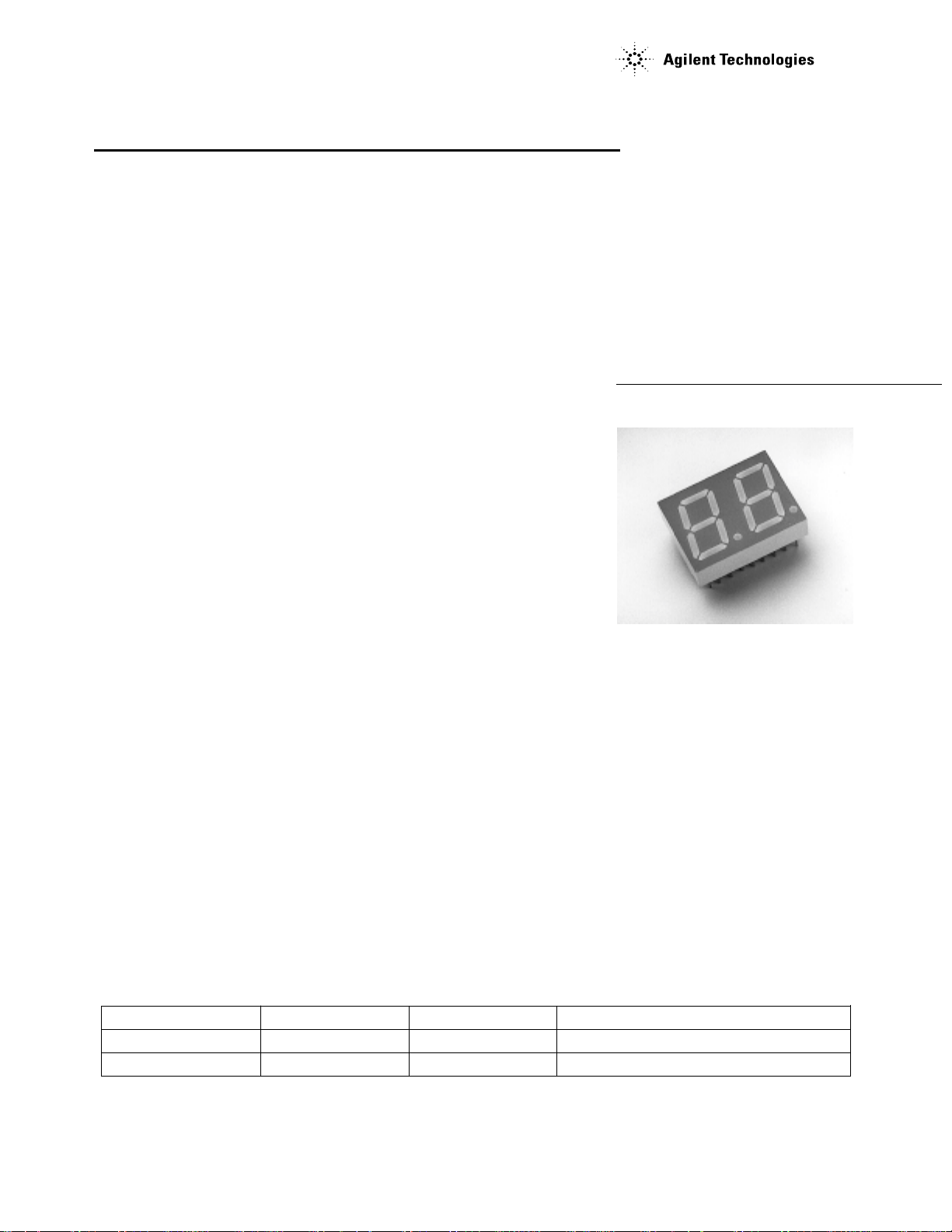
These 14.2 mm (0.56 inch) two
digit displays use industry
standard size and pin-out. The
devices are available as either
common anode or common
cathode. These gray-faced
displays are available in a choice
of high efficiency red (HER),
green, or yellow colors. The
HDSP-521x and HDSP-523x
series are suitable for indoor use.
These parts are subjected to
Outgoing Quality Assurance
(OQA) inspection with AQL of
0.065% for functional and visual/
cosmetic rejects.
Devices
HER HDSP- Green HDSP- Yellow HDSP- Description
521E 521G 521Y Common Anode Right Hand Decimal
523E 523G 523Y Common Cathode Right Hand Decimal
Notes:
1. For industrial applications, it is recommended to use HDSP-5521/5523/5621/5623/5721/5723.
2. For details, please contact your local Agilent sales office or an authorized distributor.
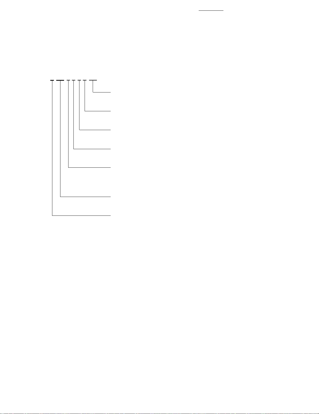
Part Numbering System
5082 -X X X X-X X X X X
HDSP-X X X X-X X X X X
2
Mechanical Options
[1]
00: No Mechanical Option
Color Bin Options
[1,2]
0: No Color Bin Limitation
Maximum Intensity Bin
[1,2]
0: No Maximum Intensity Bin Limitation
Minimum Intensity Bin
[1,2]
0: No Minimum Intensity Bin Limitation
Device Configuration/Color
[1]
E: High Efficiency Red
G: Green
Y: Yellow
Device Specific Configuration
[1]
Refer to Respective Datasheet
Package
[1]
Refer to Respective Datasheet
Notes:
1. For codes not listed in the figure above, please refer to the respective datasheet or contact your nearest
Agilent representative for details.
2. Bin options refer to shippable bins for a part number. Color and Intensity Bins are typically restricted to 1
bin per tube (exceptions may apply). Please refer to respective datasheet for specific bin limit information.
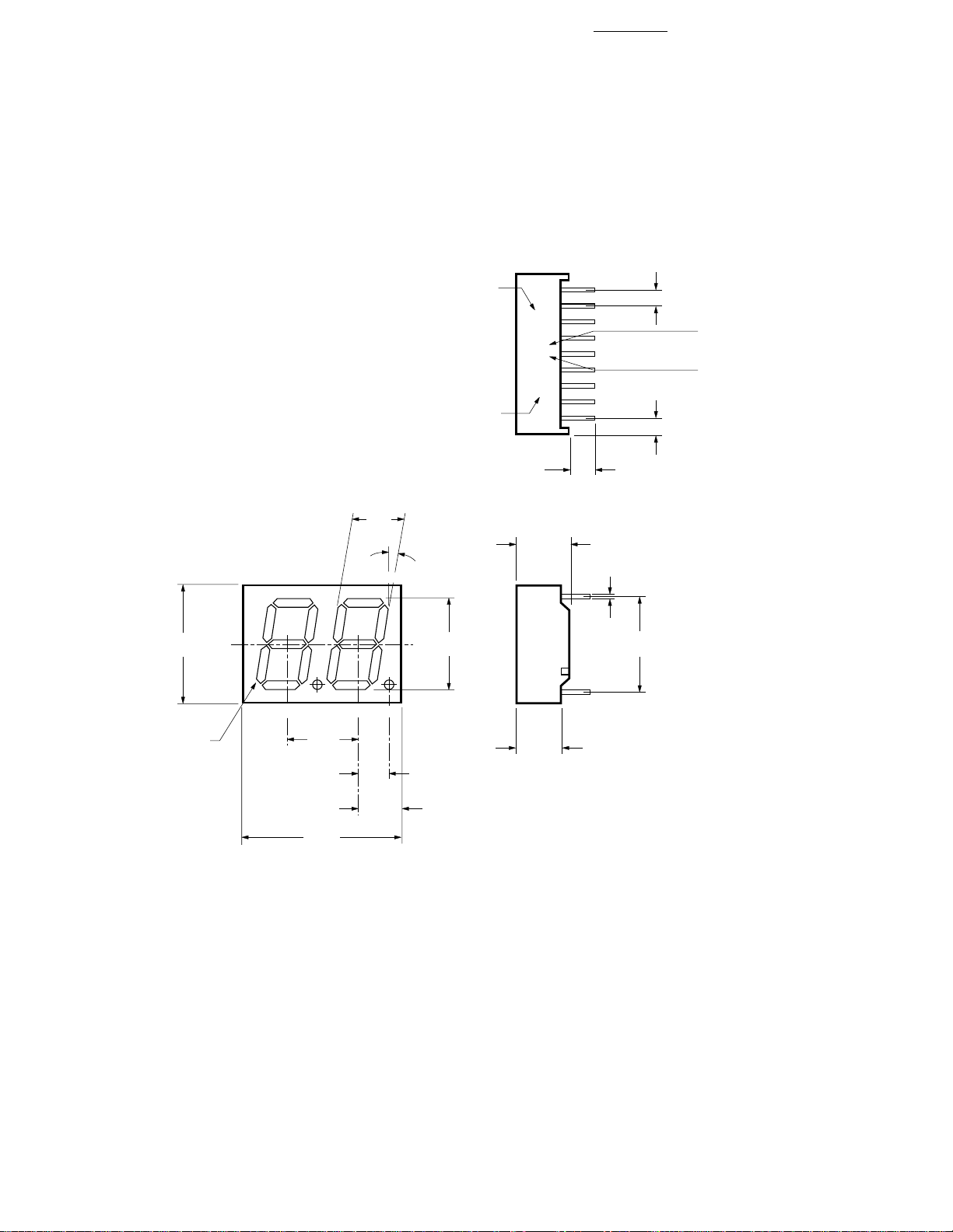
Package Dimensions
3
18.60
(0.732)
TOP END VIEW
2.54
(0.100)
COUNTRY OF ORIGIN
COLOR BINNING
(NOTE 3)
LUMINOUS
INTENSITY
CATEGORY
0.50
(0.092)
DIA.
15.24
(0.600)
2.34
HDSP-XXXX
YWW XZ COO
DATE CODE
4.27 ± 0.50
(0.168 ± 0.020)
7.80
(0.307)
10°
18
1017 16 15 14 13 12 11
14.22
(0.560)
8.00
(0.315)
(0.020)
192345678
DIGIT NO. 1
12.70
(0.500)
4.81
(0.191)
25.00
(0.984)
6.150
(0.242)
FRONT VIEW
NOTES:
1. ALL DIMENSIONS ARE IN MILLIMETERS (INCHES).
2. TOLERANCE IS 0.25 mm (0.01 INCH) UNLESS OTHERWISE STATED.
3. FOR GREEN AND YELLOW ONLY.
6.86
(0.270)
SIDE VIEW

Internal Circuit Diagram
17 16 15 14 13 12 11 10
18
4
a
b
f
g
e
123456789
17 16 15 14 13 12 11 10
18
f
e
123456789
c
d
DP
COMMON ANODE
a
b
g
c
d
DP
COMMON CATHODE
a
f
b
g
c
e
d
a
f
b
g
c
e
d
DP
DP
COMMON ANODE COMMON CATHODE
PIN
1 E CATHODE NO. 1
2 D CATHODE NO. 1
3 C CATHODE NO. 1
4 DP CATHODE NO. 1
5 E CATHODE NO. 2
6 D CATHODE NO. 2
7 G CATHODE NO. 2
8 C CATHODE NO. 2
9 DP CATHODE NO. 2
10 B CATHODE NO. 2
11 A CATHODE NO. 2
12 F CATHODE NO. 2
13 DIGIT NO. 2 ANODE 13
14 DIGIT NO. 1 ANODE 14
15 B CATHODE NO. 1 15
16 A CATHODE NO. 1 16
17 G CATHODE NO. 1 17
18 F CATHODE NO. 1 18
FUNCTION
PIN
1
2
3
4
5
6
7
8
9
10
11
12
FUNCTION
E ANODE NO. 1
D ANODE NO. 1
C ANODE NO. 1
DP ANODE NO. 1
E ANODE NO. 2
D ANODE NO. 2
G ANODE NO. 2
C ANODE NO. 2
DP ANODE NO. 2
B ANODE NO. 2
A ANODE NO. 2
F ANODE NO. 2
DIGIT NO. 2 CATHODE
DIGIT NO. 1 CATHODE
B ANODE NO. 1
A ANODE NO. 1
G ANODE NO. 1
F ANODE NO. 1

5
Absolute Maximum Ratings at T
=25°C
A
HER Green Yellow
HDSP-521E HDSP-521G HDSP-521Y
Parameter HDSP-523E HDSP-523G HDSP-523Y Units
Average Power per Segment or DP 62.5 105 45 mW
Peak Forward Current per Segment or DP 90 90 60 mA
(1/10 Duty Cycle, 0.1 ms Pulse Width)
DC Forward Current per Segment or DP
[1]
25
[1]
30
[3]
20
[2]
mA
Reverse Voltage per Segment or DP 5 5 5 V
Operating Temperature -35 to +85 -35 to +85 -35 to +85 °C
Storage Temperature -35 to +85 -35 to +85 -35 to +85 °C
Wave Soldering Temperature for 3 seconds
[4]
250 250 250 °C
(2 mm [0.063 in.] below Body)
Notes:
1. Derate above 25°C at 0.33 mA/°C.
2. Derate above 25°C at 0.27 mA/°C.
3. Derate above 40 celcius at 0.35 mA/celcius.
4. Not recommended to be soldered more than 2 times. Minimum interval between solderings is 15 minutes. Total soldering time not
to exceed 5 seconds.
Optical/Electrical Characteristics at T
=25°C
A
High Efficiency Red
Devices Test
HDSP- Parameter Symbol Min. Typ. Max. Units Conditions
Luminous Intensity/Segment I
(Segment Average)
[1,2]
Forward Voltage/Segment or DP V
521E Peak Wavelength
523E Dominant Wavelength
Reverse Voltage/Segment or DP
[3]
[4]
Temperature Coefficient of ⌬V
VF/Segment or DP
v
F
PEAK
d
V
R
F
2.28 4.00 7.69 mcd IF = 10 mA
2.05 2.60 V IF = 20 mA
640 nm
628 nm IF = 10 mA
5.0 V I
/°C -2 mV/°C
= 100 µA
R
Green
Devices Test
HDSP- Parameter Symbol Min. Typ. Max. Units Conditions
Luminous Intensity/Segment I
(Segment Average)
[1,2]
Forward Voltage/Segment or DP V
521G Peak Wavelength
523G Dominant Wavelength
Reverse Voltage/Segment or DP
[3]
[4]
Temperature Coefficient of ⌬V
VF/Segment or DP
v
F
PEAK
d
V
R
F
2.28 3.50 5.13 mcd IF = 10 mA
2.0 2.4 V IF = 10 mA
568 nm
564.5 570 576.5 nm IF = 10 mA
5.0 V I
/°C-2mV/°C
= 100 µA
R

6
Yellow
Devices Test
HDSP- Parameter Symbol Min. Typ. Max. Units Conditions
Luminous Intensity/Segment I
(Segment Average)
[1,2]
Forward Voltage/Segment or DP V
521Y Peak Wavelength
523Y Dominant Wavelength
Reverse Voltage/Segment or DP
[3]
[4]
Temperature Coefficient of ⌬V
V
/Segment or DP
F
Notes:
1. Case temperature of the device immediately prior to the intensity measurement is 25°C.
2. The digits are categorized for luminous intensity. The intensity category is designated by a letter on the side of the package.
3. The dominant wavelength, d, is derived from the CIE chromaticity diagram and represents the single wavelength which defines the
color of the device.
4. Typical specification for reference only. Do not exceed absolute maximum ratings.
v
F
PEAK
d
V
R
F
1.52 2.30 5.13 mcd IF = 10 mA
2.1 2.4 V IF = 20 mA
589 nm
582.0 587 592.0 nm IF = 10 mA
5.0 V I
/°C -2 mV/°C
= 100 µA
R
Intensity Bin Limits
[1]
(mcd at 10 mA)
Yellow GREEN HER
Bin Name Min.
[2]
Max.
[2]
Min.
[2]
Max.
[2]
Min.
F 1.52 2.28 NA NA NA NA
G 2.28 3.42 2.28 3.42 2.28 3.42
H 3.42 5.13 3.42 5.13 3.42 5.13
I NA NA NA NA 5.13 7.69
Notes:
1. Bin categories are established for classification of products. Products may not be available in all bin categories.
2. Tolerance for each bin limit is ± 10%.
Color Categories (Dominant Wavelength)
GREEN
Bin Name Min.
[2]
3 570.5 573.5
2 573.5 576.5
YELLOW
Bin Name Min.
[2]
2 587.00 589.50
3 584.50 587.00
Max.
Max.
[2]
[2]
[2]
Max.
[2]
Notes:
1. Bin categories are established for classification of products. Products may not be available
in all bin categories.
2. Tolerance for each bin limit is ± 1 nM.

7
40
35
30
25
20
15
YELLOW
10
5
0
20
– MAXIMUM DC CURRENT PER SEGMENT – mA
I
30 90 100
TA – AMBIENT TEMPERATURE – °C
DC
GREEN / HER
40 60 80
7050
Figure 1. Maximum Allowable DC
Current vs. Ambient Temperature.
4.0
3.5
3.0
2.5
2.0
1.5
1.0
(NORMALIZED AT 10 mA)
0.5
RELATIVE LUMINOUS INTENSITY
0
0
5152535
– DC FORWARD CURRENT – mA
I
F
HER, YELLOW,
GREEN
20 40
10 30
– FORWARD CURRENT PER SEGMENT – mA
F
I
90
80
70
60
50
40
30
20
10
0
1
GREEN
YELLOW
HER
35
24
V
– FORWARD VOLTAGE – V
F
Figure 2. Forward Current vs.
Forward Voltage.
1.6
1.5
1.4
1.3
1.2
1.1
1.0
0.9
– RELATIVE EFFICIENCY
0.8
V
η
0.7
0.6
0
(NORMALIZED TO 1 AT 10 mA PER SEGMENT)
I
PEAK
YELLOW
HER
GREEN
20 70 80 100
– PEAK FORWARD CURRENT
PER SEGMENT – mA
6050403010
Contrast Enhancement
For information on contrast
enhancement, please see
Application Note 1015.
Soldering/Cleaning
Cleaning agents from the ketone
family (acetone, methyl ethyl
ketone, etc.) and from the
chlorinated hydrocarbon family
(methylene chloride, trichloroethylene, carbon tetrachloride,
etc.) are not recommended for
cleaning LED parts. All of these
various solvents attack or dissolve
the encapsulating epoxies used
to form the package of plastic
LED parts.
For information on soldering
LEDs please refer to Application
Note 1027.
Device Reliability
For reliability information, please
see the reliability data sheet
14.2 mm (0.56 inch) General
Purpose Two Digit Seven
Segment Display.
90
Figure 3. Relative Luminous Intensity
vs. DC Forward Current.
Figure 4. Relative Efficiency (Luminous
Intensity per Unit Current) vs. Peak
Current.

www.agilent.com/semiconductors
For product information and a complete list of
distributors, please go to our web site.
For technical assistance call:
Americas/Canada: +1 (800) 235-0312 or
(916) 788-6763
Europe: +49 (0) 6441 92460
China: 10800 650 0017
Hong Kong: (+65) 6756 2394
India, Australia, New Zealand: (+65) 6755 1939
Japan: (+81 3) 3335-8152 (Domestic/International), or 0120-61-1280 (Domestic Only)
Korea: (+65) 6755 1989
Singapore, Malaysia, Vietnam, Thailand,
Philippines, Indonesia: (+65) 6755 2044
Taiwan: (+65) 6755 1843
Data subject to change.
Copyright © 2004 Agilent Technologies, Inc.
Obsoletes 5988-0376EN
July 17, 2004
5988-5378EN
 Loading...