


ADNS-3050
Entry-level Gaming Optical Navigation Sensor
Data Sheet
Description
The Avago Technologies ADNS-3050 is a small form factor entry-level gaming optical navigation sensor. It is housed in an 8-pin staggered dual in-line package (DIP). It is capable of high-speed motion detection typically at 60ips and acceleration up to 20g; suitable for both wired and wireless gaming navigation system. The low power management in wireless mode can be customized to suit user preferences. In addition, it has an on-chip oscillator and LED driver to minimize external components.
The ADNS-3050 sensor along with the ADNS-5110-001 lens, ADNS-5200 clip, and HLMP-EG3E red LED forms a complete and compact mouse tracking system. There are no moving parts, which translates to high reliability and less maintenance for the end user. Precision optical alignment is not required, thus facilitating high volume assembly.
Theory of Operation
The ADNS-3050 is based on Optical Navigation Technology, which measures changes in position by optically acquiring sequential surface images (frames) and mathematically determining the direction and magnitude of movement. The ADNS-3050 contains an Image Acquisition System (IAS), a Digital Signal Processor (DSP), and a four wire serial port. The IAS acquires microscopic surface images via the lens and illumination system. These images are processed by the DSP to determine the direction and distance of motion. The DSP calculates the ΔX and Δy relative displacement values. An external microcontroller reads and translates the ΔX and Δy information from the sensor serial port into PS2, USB, or RF signals before sending them to the host PC.
Features
Small Form Factor Package - 8-pin DIP
Operating Voltage: 2.8V-3.0V
High Speed Motion Detection at typical of 60ips and acceleration up to 20g.
Selectable Resolutions up to 2000cpi
Four wire Serial Port Interface
External Interrupt Output for Motion Detection
Internal Oscillator — no clock input needed
On-chip LED driver
Minimal number of passive components
Programmable power-saving modes for selectable wired or wireless application
Customizable response time and downshift time for rest modes
Configurable LED operating modes and drive current
Applications
Wired and Wireless Optical gaming mice and trackballs
Integrated input devices
Battery-powered input devices
NOTE: The ADNS-3050 sensor is not designed for use with blue LED navigation system.

Pinout of ADNS-3050 Optical Mouse Sensor
|
|
|
|
|
|
|
|
|
|
Input/ |
|
|
|
|
|
|
|
|
|
|
|
|
|||||||||
|
Pin |
Name |
|
|
|
|
|
Output |
|
|
|
|
|
Description |
|||||||||||||||||
|
|
|
|
|
|
|
|
|
|
|
|
|
|
|
|
|
|
|
|
|
|
|
|
|
|
|
|
|
|
|
|
1 |
MISO |
|
|
|
|
|
O |
|
|
|
|
|
Serial Data Output |
||||||||||||||||||
|
|
|
|
|
|
|
|
|
|
|
|
|
|
|
|
|
|
|
|
|
|
|
|
|
(Master In/Slave Out) |
||||||
|
|
|
|
|
|
|
|
|
|
|
|
|
|
|
|
|
|
|
|
|
|
|
|
|
|
|
|
|
|
|
|
2 |
LED |
|
|
|
|
|
I |
|
|
|
|
|
LED Illumination Control Input |
||||||||||||||||||
|
|
|
|
|
|
|
|
|
|
|
|
|
|
|
|
|
|
|
|
|
|
|
|
|
|
|
|
|
|
|
|
3 |
MOTION |
|
|
|
|
|
O |
|
|
|
|
|
Motion Interrupt Output |
||||||||||||||||||
|
|
|
|
|
|
|
|
|
|
|
|
|
|
|
|
|
|
|
|
|
|
|
|
|
(Active low,) |
||||||
|
|
|
|
|
|
|
|
|
|
|
|
|
|
|
|
|
|
|
|
|
|
|
|
|
|
|
|
|
|
|
|
4 |
NCS |
|
|
|
|
|
I |
|
|
|
|
|
Chip Select |
||||||||||||||||||
|
|
|
|
|
|
|
|
|
|
|
|
|
|
|
|
|
|
|
|
|
|
|
|
|
(Active low) |
||||||
|
|
|
|
|
|
|
|
|
|
|
|
|
|
|
|
|
|
|
|
|
|
|
|
|
|
|
|
|
|
|
|
5 |
SCLK |
|
|
|
|
|
I |
|
|
|
|
|
Serial Clock Input |
||||||||||||||||||
|
|
|
|
|
|
|
|
|
|
|
|
|
|
|
|
|
|
|
|
|
|
|
|
|
|
|
|
|
|
|
|
6 |
GND |
|
|
|
|
|
I |
|
|
|
|
|
Ground |
||||||||||||||||||
|
|
|
|
|
|
|
|
|
|
|
|
|
|
|
|
|
|
|
|
|
|
|
|
|
|
|
|
|
|
|
|
7 |
VDD |
|
|
|
|
|
I |
|
|
|
|
|
Supply Voltage |
||||||||||||||||||
|
|
|
|
|
|
|
|
|
|
|
|
|
|
|
|
|
|
|
|
|
|
|
|
|
|
|
|
|
|
|
|
8 |
MOSI |
|
|
|
|
|
I |
|
|
|
|
|
Serial Data Input |
||||||||||||||||||
|
|
|
|
|
|
|
|
|
|
|
|
|
|
|
|
|
|
|
|
|
|
|
|
|
(Master Out/Slave In) |
||||||
|
|
|
|
|
|
|
|
|
|
|
|
|
|
|
|
|
|
|
|
|
|
|
|
|
|
|
|
|
|
|
|
|
|
|
|
|
|
|
|
|
|
|
|
|
|
|
|
|
|
|
|
|
|
|
|
|
|
|
|
|
|
|
|
|
|
|
|
|
|
|
|
|
|
|
|
|
|
|
|
|
|
|
|
|
|
|
|
|
|
|
|
|
|
|
|
|
|
|
|
|
|
|
|
|
|
|
|
|
|
|
|
|
|
|
|
|
|
|
|
|
|
|
|
|
|
|
|
|
|
|
|
|
|
|
|
|
|
|
|
|
|
|
|
|
|
|
|
|
|
|
|
|
|
|
|
|
|
|
|
|
|
|
|
|
|
|
|
|
|
|
|
|
|
|
|
|
|
|
|
|
|
|
|
|
|
|
|
|
|
|
|
|
|
|
|
|
|
|
|
|
|
|
|
|
|
|
|
|
|
|
|
|
|
|
|
|
|
|
|
|
|
|
|
|
|
|
|
|
|
|
|
|
|
|
|
|
|
|
|
|
|
|
|
|
|
|
|
|
|
|
|
|
|
|
|
|
|
|
|
|
|
|
|
|
|
|
|
|
|
|
|
|
|
|
|
|
|
|
|
|
|
|
|
|
|
|
|
|
|
|
|
|
|
|
|
|
|
|
|
|
|
|
|
|
|
|
|
|
|
|
|
|
|
|
|
|
|
|
|
|
|
|
|
|
|
|
|
|
|
|
|
|
|
|
|
|
|
|
|
|
|
|
|
|
|
|
|
|
|
|
|
|
|
|
|
|
|
|
|
|
|
|
|
|
|
|
|
|
|
|
|
|
|
|
|
|
|
|
|
|
|
|
|
|
|
|
|
|
|
|
|
|
|
|
|
|
|
|
|
|
|
|
|
|
|
|
|
|
|
|
|
|
|
|
|
|
|
|
|
|
|
|
|
|
|
|
|
|
|
|
|
|
|
|
|
|
|
|
|
|
|
|
|
|
|
|
|
|
|
|
|
|
|
|
|
|
|
|
|
|
|
|
|
|
|
|
|
|
|
|
|
|
|
|
|
|
|
|
|
|
|
|
|
|
|
|
|
|
|
|
|
|
|
|
|
|
|
|
|
|
|
|
|
|
|
|
|
|
|
|
|
|
|
|
|
|
|
|
|
|
|
|
|
|
|
|
|
|
|
|
|
|
|
|
|
|
|
|
|
|
|
|
|
|
|
|
|
|
|
|
|
|
|
|
|
|
|
|
|
|
|
|
|
|
|
|
|
|
|
|
|
|
|
|
|
|
|
|
|
|
|
|
|
|
|
|
|
|
|
|
|
|
|
|
|
|
|
|
|
|
|
|
|
|
|
|
|
|
|
|
|
|
|
|
|
|
|
|
|
|
|
|
|
|
|
|
|
|
|
|
|
|
|
|
|
|
|
|
|
|
|
|
|
|
|
|
|
|
|
|
|
|
|
|
|
|
|
|
|
|
|
|
|
|
|
|
|
|
|
|
|
|
|
|
|
|
|
|
|
|
|
|
|
|
|
|
|
|
|
|
|
|
|
|
|
|
|
|
|
|
|
|
|
|
|
|
|
|
|
|
|
|
|
|
|
|
|
|
|
|
|
|
|
|
|
|
|
|
|
|
|
|
|
|
|
|
|
|
|
|
|
|
|
|
|
|
|
|
|
|
|
|
|
|
|
|
|
|
|
|
|
|
|
|
|
|
|
|
|
|
|
|
|
|
|
|
|
|
|
|
|
|
|
|
|
|
|
|
|
|
|
|
|
|
|
|
|
|
|
|
|
|
|
|
|
|
|
|
|
|
|
|
|
|
|
|
|
|
|
|
|
|
|
|
|
|
|
|
|
|
|
|
|
|
|
|
|
|
|
|
|
|
|
|
|
|
|
|
|
|
|
|
|
|
|
|
|
|
|
|
|
|
|
Figure 2. Package Outline Drawing
|
|
XYYWWZ |
|
|
|
|
|
|||
|
|
|
|
|
|
|
||||
5 |
SCLK |
|
|
|||||||
|
|
|
|
|
|
|
|
|||
|
|
|
|
|
|
|
|
|
|
|
6 |
GND |
|
|
|
|
|
|
|
|
|
|
|
A3050 |
||||||||
|
|
|||||||||
7 |
VDD |
|||||||||
|
|
|
|
|
|
|
|
|||
|
|
|
|
|
|
|
|
|
|
|
|
|
|
|
|
|
|
|
|
|
|
8 |
MOSI |
|
|
|
|
|
|
|
|
|
|
|
|
|
|
|
|
|
|
|
|
Pin 1
Figure 1. Package Outline Drawing (Top View)
4 NCS
3 MOTION
2 LED
1 MISO
CAUTION: It is advised that normal static precautions be taken in handling and assembling of this component to prevent damage and/or degradation which may be induced by ESD.
2
Overview of Optical Mouse Sensor Assembly
Avago Technologies provides an IGES file drawing describing the base plate molding features for lens and PCB alignment. The ADNS-3050 sensor is designed for mounting on a through-hole PCB. There is an aperture stop and features on the package that align to the lens. The ADNS-5110-001 lens provides optics for the imaging of the surface as well as illumination of the surface at the optimum angle. Features on the lens align it to the sensor, base plate, and clip with the LED. The ADNS-5200 clip holds the LED in relation to the lens. The LED must be inserted into the clip and the LED‘s leads formed prior to loading on the PCB.
The HLMP-EG3E red LED is recommended for illumination.
Notes:
1.Dimensions in millimeter/inches
2.View from component side of PCB (or top view of mouse)
Figure 3. Recommended PCB Mechanical Cutouts and Spacing
3
TOP VIEW
CROSS SECTION SIDEVIEW
Important Note: Pin 1 of sensor should be located nearest to the LED Figure 4. 2D Assembly drawing of ADNS-3050 (Top and Side View)
Note:
A – Distance from object surface to lens reference plane B – Distance from object surface to sensor reference plane
Figure 5. Distance from lens reference plane to tracking surface (Z)
4
HLMP-EG3E LED
ADNS-5200 LED Clip
ADNS-3050 (Sensor)
Customer supplied PCB
ADNS-5110-001
Customer supplied base plate with recommended alignment features per IGES drawing
Important Note: IR LED is recommended for lower power consumption.
Figure 6. Exploded View of Assembly
PCB Assembly Considerations
1.Insert the sensor and all other electrical components into PCB.
2.Insert the LED into the assembly clip and bend the leads 90 degrees.
3.Insert the LED clip assembly into PCB.
4.This sensor package is only qualified for wave-solder process.
5.Wave solder the entire assembly in a no-wash solder
process utilizing solder fixture. The solder fixture is needed to protect the sensor during the solder process. It also sets the correct sensor-to-PCB distance as the lead shoulders do not normally rest on the PCB surface. The fixture should be designed to expose the sensor leads to solder while shielding the optical aperture from direct solder contact.
6.Place the lens onto the base plate.
7.Remove the protective Kapton tape from optical aperture of the sensor. Care must be taken to keep contaminants from entering the aperture. Recommend not to place the PCB facing up during the entire mouse assembly process. Recommend to hold the PCB first vertically for the Kapton removal process.
8.Insert PCB assembly over the lens onto the base plate aligning post to retain PCB assembly. The sensor aperture ring should self-align to the lens.
5
9.The optical position reference for the PCB is set by the base plate and lens. Note that the PCB motion due to button presses must be minimized to maintain optical alignment.
10.Install mouse top case. There MUST be a feature in the top case to press down onto the PCB assembly to ensure all components are interlocked to the correct vertical height.
|
|
|
|
|
ADNS-3050 |
|
|
|
|
|
||||
|
|
|
|
|
|
|
|
|
|
|
|
|
|
|
VDD |
|
|
CONTROLAND |
|
|
|
|
|
|
|
REGISTERS |
|
|
NCS |
|
|
|
POWER |
|
|
|
|
|
|
|
ANDPORT |
|
|
SCLK |
|
|
|
|
|
|
|
|
|
|
|
|
|||
GND |
|
|
|
IMAGE ARRAY |
|
|
|
MOSI |
||||||
|
|
|
|
|
|
|
|
|
|
|
|
|
||
|
|
|
|
|
|
|
|
|
|
|
|
|
MISO |
|
|
|
|
|
|
|
|
|
|
|
|
|
|
|
|
|
|
|
|
|
|
DSP |
|
SERIAL |
|
|||||
|
|
|
|
|
|
|
|
|
||||||
|
|
|
|
|
|
|
|
|
|
|||||
LED |
|
|
DRIVE |
|
|
|
|
|
|
|
|
|
MOTION |
|
|
|
|
|
|
|
|
|
|
|
|
|
|
||
|
|
|
|
|
|
|
|
|
|
|
|
|
||
|
|
LED |
|
OSCILLATOR |
|
|
|
|
|
|||||
|
|
|
|
|
|
|
|
|||||||
|
|
|
|
|
|
|
|
|
||||||
|
|
|
|
|
|
|
|
|
|
|
|
|
|
|
|
|
|
|
|
|
|
|
|
|
|
|
|
|
|
|
|
|
|
|
|
|
|
|
|
|
|
|
|
|
Figure 7. Block diagram of ADNS-3050 optical mouse
|
|
+ |
5 |
9%86 |
|
: ' |
|
|
* ' |
|
|
% |
*1' |
|
6 |
6+,(/' |
|
|
ZD\PP+:)/ |
|
9&&
 &
&  &
& & 9X) Q) S)
5 5
5 |
5 |
5 |
5 |
9''
|
&21 |
|
|
|
||
|
|
|
|
|
|
|
|
|
|
|
|
||
|
|
|
|
|
||
|
|
|
|
|
||
|
|
|
|
|||
3&%B62&.3;(7B
9''-7$*
5
N 5 N
 &
&
Q)
|
|
|
|
|
|
|
|
|
|
9'' |
|
|
|
|
|
|
|
|
|
|
|
|
|
|
|
|
|
5 |
|
|
|
|
|
|
|
|
|
|
|
|
|
|
|
|
|
5 |
|
|
|
|
|
|
|
|
9&& |
|
|
|
|
|
|
|
|
& |
& |
|
& |
|
|
|
|
|
|
|
|
|
|
|
9'' |
|
X)9 |
Q) S) |
|
|
|
|
|||
& |
& & |
|
|
|
|
& & & |
|
|
|
|
|
|
5 |
|
|||
S) |
Q) 9X) |
|
|
|
S) Q) 9X) |
|
|
|
|
|
|
5 |
|
||||
|
|
|
|
|
|
|
|
|
|
|
|
|
|
|
|
||
|
|
|
|
|
|
|
|
|
|
|
|
|
|
|
|
8 |
' |
|
|
|
|
|
|
|
|
|
|
|
|
|
9'' |
|
|
|
('+/03 |
|
|
|
8 |
|
|
|
|
|
|
|
|
|
|
|
|
||
|
|
|
|
|
|
|
6&/. |
|
6&/. |
|
|
|
|
|
|
||
|
|
|
95(*,1 |
9'' |
|
3 6&/. |
|
|
|
|
6&/. |
|
|
|
|
||
|
|
|
|
|
0,62 |
|
0,62 |
|
|
|
|
|
|
||||
|
|
9%86 |
|
3 0,62 |
|
|
0,62 |
|
|
|
|
||||||
|
|
|
' |
|
|
3 026, |
|
026, |
|
026, |
|
|
026, |
;<B/(' |
|
||
|
|
|
|
|
|
1&6 |
|
1&6 |
|
|
|
|
|||||
|
|
' |
|
|
3 1&6 |
|
|
1&6 |
|
|
|
|
|||||
|
|
|
|
|
|
027,21 |
|
027,21 |
|
|
|
|
|
|
|||
|
|
|
|
|
|
3 |
|
|
027,21 |
|
|
|
|
||||
|
|
|
|
|
|
|
|
|
|
|
|
|
|
|
|
||
& |
& |
|
|
|
|
3 |
=% |
|
|
|
|
|
|
|
|
|
|
|
|
|
|
|
|
|
|
|
|
|
|
|
|
||||
|
|
|
|
3 |
|
|
|
|
|
|
|
|
|
||||
S) |
S) |
|
|
|
|
|
=$ |
|
|
|
|
*1' |
|
|
|
|
|
3 |
|
|
3 |
|
|
|
|
|
|
|
|
||||||
|
|
|
3 |
|
|
3 |
|
6:B/()7 |
|
|
|
|
|
|
|
|
|
|
|
|
|
|
|
6:B5,*+7 |
|
|
|
|
|
$'16 |
|
||||
|
|
|
|
& ) |
|
3 |
|
|
|
|
|
|
|||||
|
|
|
|
|
|
6:B0,' |
|
|
|
|
|
|
|
|
|
||
|
|
|
|
|
|
3 |
|
|
|
|
|
|
|
|
|
|
|
|
|
|
|
|
|
|
&3, |
|
|
|
|
|
|
|
|
|
|
|
|
|
|
|
|
3 |
|
|
|
|
|
|
|
|
|
||
|
|
|
|
|
|
|
&3, |
|
|
|
|
|
|
|
|
|
|
|
|
|
|
|
|
3 |
|
|
|
|
|
|
|
|
|
||
|
|
|
|
|
|
|
|
|
|
|
|
|
|
|
|
|
|
|
|
|
|
|
|
3 |
|
|
|
|
|
|
|
|
|
|
|
|
|
& &. 567 |
|
|
|
|
/(' |
|
|
|
|
|
|
|
|
|
|
|
|
|
|
|
|
|
|
|
|
|
|
|
|
|
|
||
|
|
3 & ' |
|
|
3 |
|
|
|
|
|
|
|
|
|
|||
|
|
|
|
|
|
/(' |
|
|
|
|
|
|
|
|
|
||
|
|
|
|
|
|
3 |
/HIW%XWWRQ |
|
|
|
|
|
|
|
|||
|
|
|
|
|
|
|
/(' |
|
|
|
|
|
|
|
|||
|
|
|
|
|
|
3 |
|
|
|
|
|
|
|
|
|
||
|
5 |
|
|
|
|
|
|
|
|
|
|
%ORFN6HQVRU$'16 |
|||||
|
|
|
|
|
3 |
|
|
|
|
|
|||||||
|
|
|
|
|
|
|
|
|
|
|
|||||||
|
N |
|
|
|
|
3 |
|
6: |
|
|
|
|
|
|
|
|
|
|
|
|
|
|
|
|
|
|
|
|
|
|
|
|
|||
|
|
|
|
|
|
3 |
|
|
|
|
|
|
|
|
|||
|
|
|
|
|
|
|
|
|
|
|
|
|
|
|
|
|
|
|
|
|
|
|
|
|
|
|
|
|
|
|
|
|
|
|
|
|
|
|
|
*1' |
|
3 |
|
|
|
|
|
|
|
|
|
|
|
|
|
|
|
|
|
|
|
|
|
|
|
|
|
|
|
||
|
|
|
|
|
3 |
|
|
|
|
|
|
|
|
|
|
||
|
|
|
|
|
|
|
|
|
5LJKW%XWWRQ |
|
|
|
|
|
|
|
|
|
|
|
|
|
|
0&8 |
|
|
|
|
|
|
|
|
|
|
|
|
|
|
|
|
|
|
|
6: |
|
|
|
|
|
|
|
|
|
|
|
|
|
|
|
|
|
|
|
9'' |
|
|
|
|
|
|
|
|
|
|
|
|
|
|
|
|
|
|
|
|
&21 |
|
|
|
|
|
|
|
|
|
|
|
|
|
|
|
|
|
|
|
|
|
|
|
|
|
|
|
|
|
|
|
|
|
&3, |
|
|
|
|
/(' |
|
|
|
|
|
|
|
|
|
|
|
|
|
|
|
|
|
||
|
|
|
|
|
|
|
|
|
|
|
&3, |
|
|
|
|
/(' |
|
|
|
|
|
|
|
|
|
|
0LGGOH%XWWRQ |
|
|
|
|
|
/(' |
|
|
|
|
|
(QFRGHU= |
|
|
|
|
|
|
|
|
|
|||||
|
|
|
|
|
6: |
|
|
3&%B62&.3;(7B |
|
|
|
||||||
|
|
|
|
|
|
|
|
|
|
|
|
|
|
||||
|
|
|
|
|
|
3 |
|
|
|
|
|
|
|
|
|
|
|
|
|
|
|
|
|
|
|
|
|
|
|
|
|
|
|
|
|
=$ 3
&211(&7723&%
=% 3
3&%72&211(&7
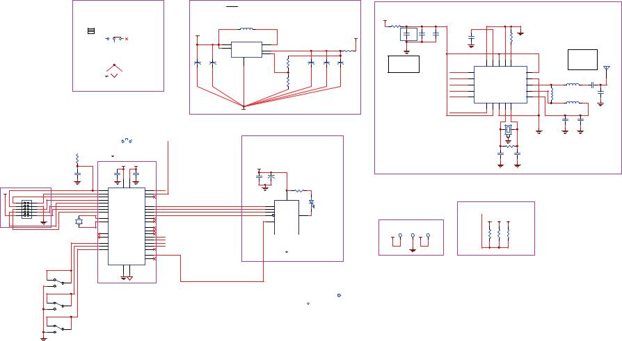
Figure 8. Schematic diagram for interface between ADNS-3050 and microcontroller with HLMP-EG3E Red LED on a corded solution NOTE: The ADNS-3050 Optical Mouse Sensor is not designed for use with blue LED navigation system.
6
|
|
|
|
|
|
|
|
|
|
|
Notes: |
|
|||||||||
|
|
|
|
|
|
|
|
|
|
|
Pads for current |
|
|||||||||
|
|
|
9%$7 |
|
|
|
|
|
measurement. |
|
|||||||||||
|
|
|
|
|
|
|
|
Short by default. |
|
||||||||||||
|
|
|
|
|
|
|
|
|
|
|
|
|
|
|
|
|
|
|
|
|
|
|
|
P1 |
|
|
|
|
|
|
|
|
|
|
|
|
|
|
|
|
|
|
|
|
|
|
|
|
|
|
|
|
|
|
|
|
|
|
|
|
|
|
|
||
|
|
PAD2 |
|
|
|
SW1 |
|
|
|
|
|
|
|
|
|
|
|
||||
|
|
|
|
|
|
SW SLIDE-SPDT |
|||||||||||||||
|
|
|
|
|
|
|
|
|
|
|
|
|
|
|
|
|
|
|
|||
|
|
|
|
21 |
% |
|
2)) |
|
|
|
|||||||||||
|
|
|
|
|
|
|
|
|
|
|
|
|
|
|
|
|
|
|
|||
|
|
|
|
|
BT1 |
|
|
|
|
|
|
|
|
|
|
|
|
|
|
|
|
|
|
|
|
|
|
|
|
|
|
|
|
|
|
|
|
|
|
|
|
|
|
|
|
|
|
BATTERY |
|
|
|
|
|
|
|
|
|
|
|
|
|
||||
|
|
|
|
|
|
% |
|
|
|
|
|
|
|
|
|
|
|
|
|||
|
|
|
|
|
|
|
|
|
|
|
|
|
|
|
|
|
|
|
|||
|
|
|
|
|
|
|
|
|
|
|
|
|
|
|
|
|
|
|
|
||
|
|
|
|
|
|
|
|
|
|
|
|
|
|
|
|
|
|
|
|
|
|
|
|
|
|
|
|
|
|
|
|
|
*1' |
|
|
|
|
|
|
||||
|
|
|
|
|
|
%DWWHU\$[$ |
|||||||||||||||
|
|
|
|
|
|
|
|
|
|
|
SW5 |
||||||||||
|
|
|
|
|
|
|
|
|
|
|
|
|
|
|
|
|
|
|
|||
|
|
|
|
|
|
|
|
|
|
|
|
|
|
||||||||
9'' |
|
|
|
|
|
|
|
|
&3, |
|
|
|
|||||||||
|
|
|
|
|
|
|
|
|
|
|
|
|
|
|
|
|
|
|
|
|
|
|
|
|
|
|
|
|
|
|
|
|
|
|
|
|
|
|
|
|
|
|
|
|
|
R3 |
|
|
|
|
|
|
|
|
|
100k |
|
9'' |
9'' |
|
|
||
|
|
|
|
|
|
||||
|
|
C2 |
|
C3 |
|
|
C4 |
|
|
|
|
10nF |
|
|
|
|
|
||
|
|
|
100nF |
|
|
100nF |
|
|
|
|
|
|
|
|
|
|
|
||
|
|
|
|
|
|
|
|
|
|
|
|
|
|
U2 |
|
|
|
|
|
|
|
|
3 |
'9&& |
$9&& |
3 |
RF_IRQ |
||
|
|
|
|
|
|
||||
9'' |
|
|
|
567 |
|
|
3 |
|
SW_CPI+ |
|
|
|
|
|
|
||||
|
J1 |
|
|
3 |
|
|
3 |
|
|
|
|
3 7&. |
|
|
|
|
|
||
|
|
|
|
|
|
|
|
|
|
|
3 706 |
|
|
|
|
|
|||
|
|
|
|
|
|
|
|
MISO_MCU |
|
|
3 7', |
|
|
3 0,62 |
|||||
|
|
|
|
|
|
|
MOSI_MCU |
||
|
3 7'2 |
|
|
3 026, |
|||||
|
|
|
|
|
|
|
SCLK_MCU |
||
|
767 |
|
|
3 6&/. |
|||||
|
|
|
|
|
|
|
NCS_MCU |
||
|
|
|
|
2274 |
3 |
||||
|
|
|
|
|
|
|
|
||
|
X2 |
;287 3 |
3 |
|
|||||
|
|
|
|
||||||
-&RQQHFWRU7$* |
32.768KHz |
|
;,1 3 |
|
MSP430- |
3 |
|
|
|
|
|
|
|
|
|
|
|
||
|
|
|
|
|
|
|
3 |
|
|
|
|
|
|
|
|
|
|
|
|
|
|
|
|
|
|
|
3 |
|
|
|
|
|
3 5;' |
|
|
3 |
|
||
|
|
|
|
|
|
|
RF_EN |
||
|
|
|
3 7;' |
|
|
3 |
|||
|
|
|
|
|
|
|
RF_NCS |
||
|
|
|
|
|
|
|
3 |
||
|
|
SW_LEFT |
|
|
|
|
|
ZA |
|
|
|
3 |
|
|
3 |
||||
|
|
SW_RIGHT |
|
|
|
|
ZB |
||
|
|
3 |
|
|
3 |
||||
|
|
SW_MID |
|
|
|
|
|
||
|
|
3 |
|
|
3 |
|
|||
|
|
|
|
|
|
|
3$ |
|
MOT_MCU |
|
|
|
|
|
'966 |
$966 |
|
|
|
|
|
|
|
|
3$ |
|
|||
|
|
|
|
|
|
|
|||
|
|
|
|
|
|
|
|
|
|
|
|
SW2 |
|
|
|
|
|
|
|
|
|
|
|
|
|
|
|
|
|
|
|
|
|
|
0&8 |
|
|
|
|
|
/HIW%XWWRQ |
|
|
|
|
|
|||
|
|
|
|
|
|
|
|
||
|
|
SW3 |
|
|
|
|
|
|
|
|
|
|
|
|
|
|
|
|
|
|
|
|
|
|
|
|
|
|
|
|
5LJKW%XWWRQ |
|
|
|
|
|
|
|
|
|
|
SW4 |
|
|
|
|
|
|
|
|
|
|
|
|
|
|
|
|
|
|
|
|
|
|
|
|
|
|
|
|
|
|
|
|
|
|
|
|
|
|
0LGGOH%XWWRQ |
|
|
|
|
|
|
|
|
NOTE:
R1= R2 x {(Vo/Vfb) -1}
R1 = 215K x {(Vo/500mV) -1}
L1
4.7uH
9%$7 |
|
|
|
|
|
|
|
|
|
U1 |
|
|
|
|
9 |
|
|
TPS61070 |
|
|
|
|
|
|
|
9%$7 |
6: |
|
|
|
|
|
|
|
|
|
|
||
|
(1 |
|
|
|
|
R6 |
|
|
|
9287 |
|
|
|
||
|
|
*1' |
|
|
|
||
|
|
|
|
|
1R |
||
|
|
)% |
|
|
|||
|
|
|
|
R1 |
|
|
|
C1 |
C5 |
|
|
1M |
C6 |
C7 |
C8 |
|
|
||||||
4.7uF/6.3V |
4.7uF/6.3V |
|
|
|
4.7uF/6.3V 4.7uF/6.3V |
10uF/6.3V |
|
|
|
|
|
R2 |
|
|
|
|
|
|
|
215k |
|
|
|
*1'
%ORFN6XSSO\9
PCB Notes: pin
9,24,34,25,26,28,11,17,18, 19, need to short track if need to connect to GND plane.
9''
C11 |
C9 |
100nF 4.7uF/6.3V
|
|
|
R5 |
|
|
|
|
33R |
|
|
|
|
U5 |
D5 |
|
0,62 |
9'' |
|
HLMP-ED80 |
|
|
|||
|
026, |
|
|
|
|
|
|
|
|
6&/. |
|
|
|
|
|
|
|
|
|
1&6 |
|
;<B/(' |
||
|
|
|
027,21
|
*1' |
|
|
|
|
|
|
|
|
|
|
ADNS 3050 |
||
|
|
|
|
|
|
|
|
|
|
|
|
|
|
|
%ORFN6HQVRU$
|
|
|
|
|
Q1 |
|
|
|
ZB |
|
&20 |
|
|
|
% |
||
|
|
|
ZA |
|
|
|
|
|
|
|
$ |
|
|
|
|
|
|
(QFRGHU=
9'' |
R12 |
|
|
|
|
|
|
|
|
|
|
|
|
|
|
|
|
|
|
5.6R |
|
|
|
|
|
|
|
|
|
|
|
|
|
|
|
|
|
2SWLRQDO |
C17 |
C18 |
C19 |
|
|
|
|
|
|
|
|
|
|
|
|
|
|
|
|
|
10uF/6.3V |
10nF |
1nF |
|
C20 |
|
|
|
|
|
R15 |
|
|
|
|
|
|
|
|
|
|
|
|
33nF |
|
|
|
|
|
22k |
|
|
|
|
|
|
|
|
|
|
|
|
|
|
|
|
|
|
|
|
|
|
Notes: |
|
|
|
Notes: |
|
|
|
|
|
|
|
|
|
|
|
|
|
|
1. 50 ohm trace |
|
|
|
|
|
|
|
|
|
|
|
|
|
|
|
|
|
(highlighted trace) |
|
||
|
10uF input cap |
|
|
|
|
|
|
|
|
|
E1 |
|||||||
|
|
|
|
|
|
|
|
|
|
|
|
U7 |
|
|
|
|
||
|
optional |
|
|
|
|
|
|
|
|
|
|
|
|
|
|
|
|
|
|
|
|
|
|
|
966 |
'9'' |
9'' |
966 |
,5() |
|
|
|
|
|
|
|
|
|
|
|
|
RF_EN |
|
&( |
|
9'' |
|
|
|
|
|
|||||
|
|
|
|
|
|
|
|
|
|
|
|
|
|
|
|
|
||
|
|
|
|
RF_NCS |
|
&61 |
|
|
|
|
|
|
966 |
|
|
L4 |
C23 |
|
|
|
|
|
|
|
|
|
|
|
|
|
|
|
3.9nH |
1.5pF |
|
||
|
|
|
|
SCLK_MCU |
|
6&/. |
|
|
nRF24L01 |
|
|
$17 |
|
|
|
|
|
|
|
|
|
|
|
|
|
|
|
|
|
|
|
|
|
|
|
||
|
|
|
|
MOSI_MCU |
|
026, |
|
|
|
|
|
|
$17 |
|
|
|
|
|
|
|
|
|
|
|
|
|
|
|
|
|
|
L3 |
|
|
C24 |
||
|
|
|
|
|
|
|
|
|
|
|
|
|
|
|
|
|
||
|
|
|
|
MISO_MCU |
0,62 |
|
9'' |
966 |
;& |
;& |
9''B3$ |
8.2nH |
L5 |
|
1pF |
|||
|
|
|
|
|
|
|
,54 |
|
|
|
|
2.7nH |
|
|
||||
|
|
|
|
RF_IRQ |
|
|
|
|
|
|
|
|
|
|
|
|
|
|
|
|
|
|
|
|
|
|
|
|
|
|
|
|
|
|
|
|
|
|
|
|
|
|
|
|
|
|
|
|
|
|
|
|
|
C25 |
C26 |
|
|
|
|
|
|
|
|
|
|
|
|
|
|
|
|
|
2.2nF |
4.7pF |
|
|
|
|
|
|
|
|
|
|
|
|
|
|
X1 |
|
|
|
|
|
|
|
|
|
|
|
|
|
|
|
|
|
|
16MHz |
|
|
|
|
|
|
|
|
|
|
|
|
|
|
|
|
|
|
|
|
|
|
|
|
|
|
|
|
|
|
|
|
|
|
|
|
|
R16 |
|
|
|
|
|
|
|
|
|
|
|
|
|
|
|
|
|
|
1M 1% |
|
|
|
|
|
|
|
|
|
|
|
|
|
C21 |
|
|
|
C22 |
|
|
|
|
|
|
|
|
|
|
|
|
|
|
22pF |
|
|
|
22pF |
|
|
|
|
|
|
|
|
|
|
|
|
|
*K]5)7UDQFHLYHU%ORFN |
|
|
|
|
|||||||
9 |
VDD1: MCU Supply |
|
VDD2: RF Supply |
||
|
|
VDD3: Sensor Supply |
|
|
|
0&8 |
5) 6(1625 |
|
|
|
|
9'' |
9'' |
9'' |
9%$7 *1' |
9 |
|
|
|
|
TP1 |
TP2 |
TP3 |
R7 |
R8 |
R9 |
|
|
|
|||
9%$7 |
|
9 |
1R |
1R |
1R |
|
|
|
|
||
|
|
|
|
|
|
9ROWDJH0HDVXUHPHQW |
&XUUHQW0HDVXUHPHQW |
||||
Figure 9. Schematic diagram for interface between ADNS-3050 and microcontroller with HLMP-EG3E Red LED on a wireless solution NOTE: The ADNS-3050 Optical Mouse Sensor is not designed for use with blue LED navigation system.
7

Design Considerations for Improved ESD Performance
For improved electrostatic discharge performance, typical creepage and clearance distance are shown in the table below. Assumption: base plate construction is as per the Avago Technologies’ supplied IGES file and ADNS-5110- 001 lens. Note that the lens material is polycarbonate or polystyrene HH30. Therefore, cyanoacrylate based adhesives or other adhesives that may damage the lens should NOT be used.
ADNS-5110-001 Lens |
Typical Distance (mm) |
Creepage |
15.43 |
|
|
Clearance |
7.77 |
|
|
Table 1. Absolute Maximum Ratings
Regulatory Requirements
Passes FCC B and worldwide analogous emission limits when assembled into a mouse with shielded cable and following Avago’s recommendations.
Passes IEC-1000-4-3 radiated susceptibility level when assembled into a mouse with shielded cable and following Avago’s recommendations.
Passes EN61000-4-4/IEC801-4 EFT tests when assembled into a mouse with shielded cable and following Avago recommendations.
Provides sufficient ESD creepage/clearance distance to withstand discharge up to 15KV when assembled into a mouse according to usage instructions above.
Parameter |
Symbol |
Minimum |
Maximum |
Units |
Notes |
Storage Temperature |
TS |
-40 |
85 |
C |
|
Operating Temperature |
TA |
-15 |
55 |
C |
|
Lead Solder Temperature |
TSOLDER |
|
260 |
C |
For 7 seconds, 1.6mm below seating plane. |
Supply Voltage |
VDD |
-0.5 |
3.7 |
V |
|
ESD (Human Body Model) |
|
|
2 |
kV |
All pins |
|
|
|
|
|
|
Input Voltage |
VIN |
-0.5 |
VDD + 0.5 |
V |
All I/O pins |
Output Current |
Iout |
|
7 |
mA |
MISO pin |
Table 2. Recommended Operating Condition
Parameter |
Symbol |
Min |
Typ. |
Max |
Units |
Notes |
Operating Temperature |
TA |
0 |
|
40 |
C |
|
Power Supply Voltage |
VDD |
2.8 |
|
3.0 |
V |
|
Power Supply Rise Time |
tRT |
0.005 |
|
100 |
ms |
0 to VDD min |
|
|
|
|
|
|
|
Supply Noise (Sinusoidal) |
VNA |
|
|
100 |
mVp-p |
10kHz —50MHz |
Serial Port Clock Frequency |
fSCLK |
|
|
1 |
MHz |
50% duty cycle |
Distance from Lens Reference |
Z |
2.3 |
2.4 |
2.5 |
mm |
|
|
|
|
|
|
|
|
Plane to Tracking Surface |
|
|
|
|
|
|
|
|
|
|
|
|
|
Speed |
S |
|
60 |
|
ips |
|
|
|
|
|
|
|
|
Acceleration |
A |
|
|
20 |
g |
In run mode |
|
|
|
|
|
|
|
Load Capacitance |
Cout |
|
|
100 |
pF |
MISO |
8

Table 3. AC Electrical Specifications
Electrical characteristics over recommended operating conditions. Typical values at 25 °C, VDD = 2.8 V.
Parameter |
Symbol |
Min. |
Typ. |
Max. |
Units |
Notes |
Motion Delay after Reset |
tMOT-RST |
|
|
50 |
ms |
From RESET register write to valid motion |
Power Down |
tPD |
|
|
50 |
ms |
From PD active to low current (when bit 1 |
|
|
|
|
|
|
of register 0x0d is set) |
Wake from Power Down |
tWAKEUP |
50 |
|
55 |
ms |
From PD inactive to valid motion (when |
|
|
|
|
|
|
write 0x5a to register 0x3a) |
MISO Rise Time |
tr-MISO |
|
40 |
200 |
ns |
CL = 100 pF |
MISO Fall Time |
tf-MISO |
|
40 |
200 |
ns |
CL = 100 pF |
MISO Delay after SCLK |
tDLY-MISO |
|
|
120 |
ns |
From SCLK falling edge to MISO data valid, |
|
|
|
|
|
|
no load condition |
|
|
|
|
|
|
|
MISO Hold Time |
thold-MISO |
500 |
|
1/fSCLK |
ns |
Data held until next falling SCLK edge |
MOSI Hold Time |
thold-MOSI |
200 |
|
|
ns |
Amount of time data is valid after SCLK |
|
|
|
|
|
|
rising edge |
|
|
|
|
|
|
|
MOSI Setup Time |
tsetup-MOSI |
120 |
|
|
ns |
From data valid to SCLK rising edge |
SPI Time between |
tSWW |
30 |
|
|
μs |
From rising SCLK for last bit of the first data |
Write Commands |
|
|
|
|
|
byte, Commands to rising SCLK for last bit |
|
|
|
|
|
|
of the second data byte |
|
|
|
|
|
|
|
SPI Time between |
tSWR |
20 |
|
|
μs |
From rising SCLK f or last bit of the first |
Write and Read Command |
|
|
|
|
|
data byte, to rising SCLK for last bit of the |
|
|
|
|
|
|
second address byte |
|
|
|
|
|
|
|
SPI Time between Read and |
tSRW |
250 |
|
|
ns |
From rising SCLK for last bit of the first data |
Subsequent Commands |
tSRR |
|
|
|
|
byte, to falling SCLK for the first bit of the |
|
|
|
|
|
|
next address |
|
|
|
|
|
|
|
SPI Read Address-Data Delay |
tSRAD |
4 |
|
|
μs |
From rising SCLK for last bit of the address |
|
|
|
|
|
|
byte, to falling SCLK for first bit of data |
|
|
|
|
|
|
being read |
|
|
|
|
|
|
|
NCS to SCLK Active |
tNCS-SCLK |
120 |
|
|
ns |
From NCS falling edge to first SCLK falling |
|
|
|
|
|
|
edge |
|
|
|
|
|
|
|
SCLK to NCS Inactive |
tSCLK-NCS |
120 |
|
|
ns |
From last SCLK rising edge to NCS rising |
(for Read Operation) |
|
|
|
|
|
edge, for valid MISO data transfer |
SCLK to NCS Inactive |
tSCLK-NCS |
20 |
|
|
μs |
From last SCLK rising edge to NCS rising |
(for Write Operation) |
|
|
|
|
|
edge, for valid MOSI data transfer |
NCS to MISO high-Z |
tNCS-MISO |
|
|
250 |
ns |
From NCS rising edge to MISO high-Z state |
Transient Supply Current |
IDDT |
|
|
60 |
mA |
Max supply current during a VDD ramp |
|
|
|
|
|
|
from 0 to VDD |
|
|
|
|
|
|
|
9
 Loading...