

Page 1
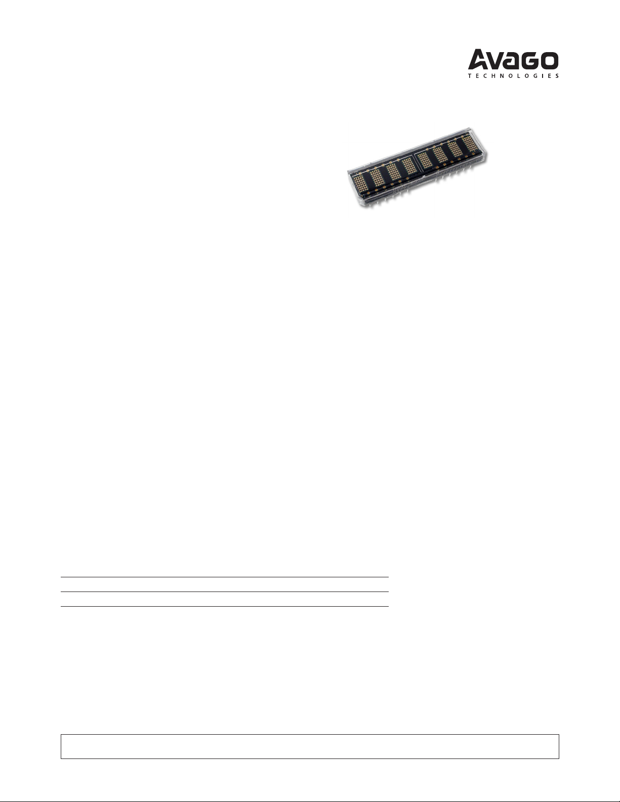
HDSP-253x Series
Eight Character 5 mm Smart Alphanumeric Display
Data Sheet
Description
The HDSP-253x is ideal for applications where displaying
eight or more characters of dot matrix information in an
aesthetically pleasing manner is required. These devices
are eight-digit, 5 x 7 dot matrix, alphanumeric displays.
The 5.0 mm (0.2 inch) high characters are packaged in a
0.300 inch (7.62 mm) 30 pin DIP. The on-board CMOS IC
has the ability to decode 128 ASCII characters, which are
permanently stored in ROM. In addition, 16 programmable
symbols may be stored in on-board RAM. Seven brightness
levels provide versatility in adjusting the display intensity
and power consumption. The HDSP-253x is designed for
standard microprocessor interface techniques. The display
and special features are accessed through a bidirectional
eight-bit data bus.
Features
• XY stackable
• 128 character ASCII decoder
• Programmable functions
• 16 user denable characters
• Multi-level dimming and blanking
• TTL compatible CMOS IC
• Wave solderable
Applications
• Avionics
• Computer peripherals
• Industrial instrumentation
• Medical equipment
• Portable data entry devices
• Telecommunications
• Test equipment
Device Selection Guide
AlGaAs Red HER Orange Yellow Green
HDSP-2534 HDSP-2532 HDSP-2530 HDSP-2531 HDSP-2533
ESD WARNING: Normal CMOS handling precautions should be observed to avoid static discharge.
Page 2
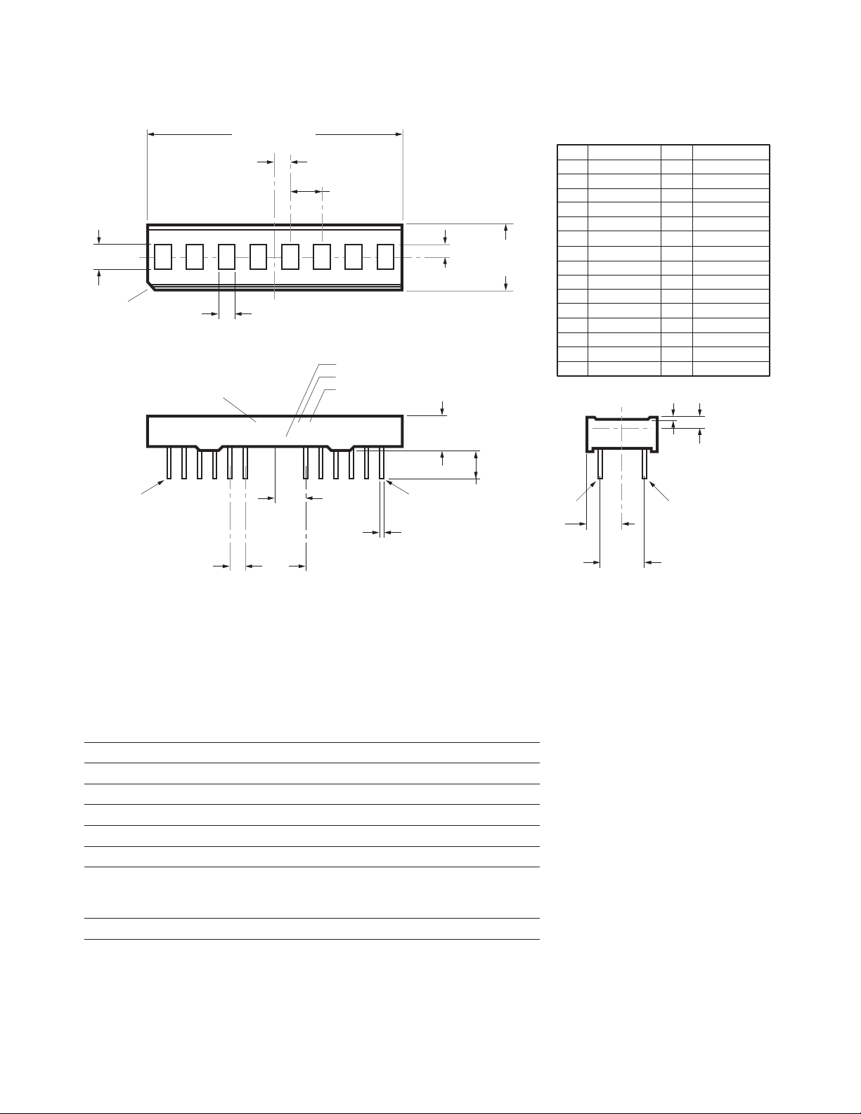
Package Dimensions
PIN # 15
SYM.
TYP.
DATE CODE (YEAR, WEEK)
LUMINOUS INTENSITY CATEGORY
COLOR BIN (3)
3.81
(0.150)
PIN # 16
1.52
(0.060)
5.31
(0.209)
2.29
(0.090)
4.57
(0.180)
[4]
4.01
(0.158)
SYM.
5.08
(0.200)
10.16
(0.400)
TYP.
0.46 0.13
(0.018 0.005)
TYP.
PIN #1
PART NUMBER
2.54 0.13
(0.100 0.005)
(TOL. NON ACCUM.)
7.62
(0.300)
REF.
0.25
(0.010)
PIN # FUNCTION PIN # FUNCTION
1
2
3
4
5
6
7
8
9
10
11
12
13
14
15
RST
FL
A0
A1
A2
A3
NO PIN
NO PIN
NO PIN
A4
CLS
CLK
WR
CE
V
DD
16
17
18
19
20
21
22
23
24
25
26
27
28
29
30
GND (SUPPLY)
THERMAL TEST
GND (LOGIC)
RD
D0
D1
NO PIN
NO PIN
NO PIN
D2
D3
D4
D5
D6
D7
PIN FUNCTION ASSIGNMENT TABLE
3 4 5 6 7
TYP.
SYM.
11.43
(0.450)
MAX.
TYP.
2.54
(0.100)
SYM.
2.68
(0.105)
42.93 (1.690) MAX.
TYP.
5.36
(0.211)
PIN #15
PIN #1 IDENTIFIER
HDSP-253x X Z
YYWW
210
Notes:
1. Dimensions are in mm (inches).
2. Unless otherwise specied, tolerance on dimensions is ±0.25 mm (0.010 inch).
3. For yellow and green displays only.
4. Marking is on side opposite pin 1.
Absolute Maximum Ratings
Supply Voltage, VDD to Ground
Operating Voltage, VDD to Ground
Input Voltage, Any Pin to Ground -0.3 V to VDD +0.3 V
Free Air Operating Temperature Range, T
Relative Humidity (Noncondensing) 85%
Storage Temperature Range, TS -55°C to 100°C
Soldering Temperature [1.59 mm (0.063 in.) Below Body]
Solder Dipping 260°C for 5 secs
Wave Soldering 250°C for 3 secs
ESD Protection @ 1.5 kΩ, 100 pF 4 kV (each pin)
Notes:
1. Maximum voltage is with no LEDs illuminated.
2. 20 dots ON in all locations at full brightness.
3. See Thermal Considerations section for information about operation in high temperature
ambients.
2
[1]
-0.3 V to 7.0 V
[2]
5.5 V
A
[3 ]
-40°C to + 85°C
Page 3
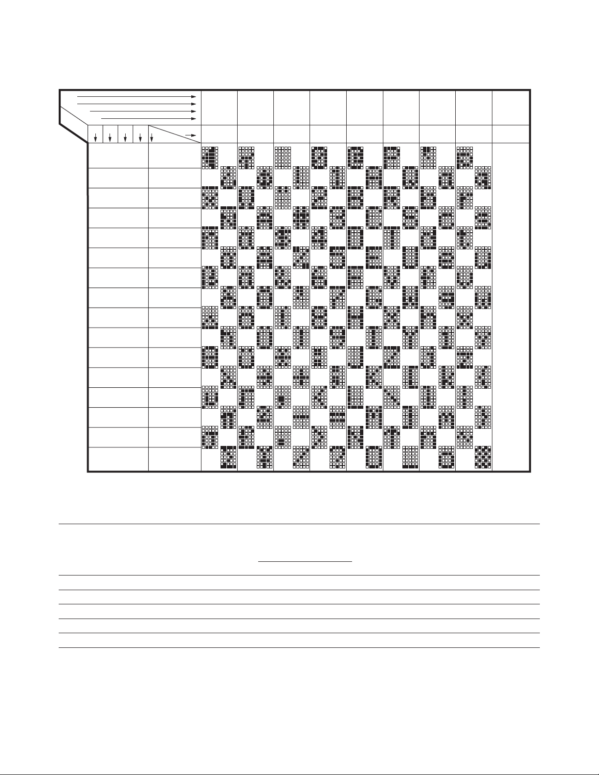
ASCII Character Set
D7
D6
D5
D4
BIT
S
D3 D0D2 D1
ROW
COLUMN
0000 0
0001 1
0010 2
0011 3
0100 4
0101 5
0110 6
0111 7
1000 8
1001 9
1010 A
1011 B
1100 C
1101 D
1110 E
1111 F
0
0
0
0
0
0
0
0
1
1
0
0
1
0
2
0
0
1
1
3
0
1
0
0
4
0
1
0
1
5
0
1
1
0
6
0
1
1
1
7
1
X
X
X
8–F
16
U
S
E
R
D
E
F
I
N
E
D
C
H
A
R
A
C
T
E
R
S
Optical Characteristics at 25°C
VDD = 5.0 V at Full Brightness
Luminous Intensity Peak Dominant
Character Average (#) Wavelength Wavelength
IV (mcd) l
LED Color Part Number Min. Typ. Typ. Typ.
AlGaAs Red HDSP-2534 5.1 25 645 637
High Eciency Red HDSP-2532 2.5 7.5 635 626
Orange HDSP-2530 2.5 7.5 600 602
Yellow HDSP-2531 2.5 7.5 583 585
Green HDSP-2533 2.5 7.5 568 574
Notes:
1. Refers to the initial case temperature of the device immediately prior to measurement.
2. Dominant wavelength, ld, is derived from the CIE chromaticity diagram, and represents the single wavelength which denes the color of the device.
[1]
PEAK
(nm) ld (nm)
[2]
3
Page 4

Recommended Operating Conditions
Parameter Symbol Minimum Nominal Maximum Units
Supply Voltage VDD 4.5 5.0 5.5 V
Electrical Characteristics over Operating Temperature Range
4.5 < VDD < 5.5 unless otherwise specied
25°C 25°C
Parameter Symbol Min. Typ.
Input Leakage II -1.0 1.0 mA VIN = 0 to VDD, Pins CLK,
(Input without Pull-up) D0-D7, A0-A
Input Current IIP -30 -11 -18 0 mA VIN = 0 to VDD, Pins CLS,
(Input with Pull-up) RST, WR, RD, CE, FL
I
Blank IDD(BL) 0.5 3.0 4.0 mA VIN = V
DD
IDD 8 Digits 12 Dots/Char
(AlGaAs)
IDD 8 Digits 20 Dots/Char
(AlGaAs)
IDD 8 Digits 12 Dots/Char
(All Colors Except AlGaAs)
IDD 8 Digits 20 Dots/Char
(All Colors Except AlGaAs)
Input Voltage High VIH 2.0 VDD V
+0.3 V
Input Voltage Low VIL GND 0.8 V
-0.3 V
Output Voltage High VOH 2.4 V VDD = 4.5 V, IOH = -40 µA
Output Voltage Low D0-D7 VOL 0.4 V VDD = 4.5 V, IOL = 1.6 mA
Output Voltage Low CLK VOL 0.4 V V
Thermal Resistance IC Rq
Junction-to-PIN
Notes:
1. VDD = 5.0 V.
2. See Thermal Considerations Section for information about operation in high temperature ambients.
3. Average IDD measured at full brightness. See Table 2 in Control Word Section for IDD at lower brightness levels. Peak IDD = 28/15 x IDD(#).
4. Maximum IDD occurs at -55°C.
[2,3,4]
IDD(V) 230 295 390 mA “V” On in All 8 Locations
[2,3,4]
IDD(#) 330 410 480 mA “#” On in All 8 Locations
[2,3,4]
IDD(V) 200 255 330 mA “V” On in All 8 Locations
[2,3,4]
IDD(#) 300 370 430 mA “#” On in All 8 Locations
16 °C/W Measured at Pin 17
J-PIN
[1]
Max.
[1]
Max. Units Test Conditions
DD
= 4.5 V, IOL = 40 µA
DD
4
4
Page 5

AC Timing Characteristics over Temperature Range
VDD = 4.5 to 5.5 V unless otherwise specied.
Reference
Number Symbol Description Min.
1 t
Write 210
Read 230 ns
2 t
3 tCE Chip Enable Active Time
Write 140
Read 160 ns
4 t
5 t
6 t
Write 140
Read 160 ns
7 t
8 tW Write Active Time 100 ns
9 tWD Data Valid Prior to Rising Edge of Write Signal 50 ns
10 tDH Data Write Hold Time 20 ns
11 tR Chip Enable Active Prior to Valid Data 160 ns
12 tRD Read Active Prior to Valid Data 75 ns
13 tDF Read Data Float Delay 10 ns
tRC Reset Active Time
Notes:
1. Worst case values occur at an IC junction temperature of 125°C.
2. For designers who do not need to read from the display, the Read line can be tied to VDD and the Write and Chip Enable lines can be tied
together.
3. Changing the logic levels of the Address lines when CE = “0” may cause erroneous data to be entered into the Character RAM, regardless of the
logic levels of the WR and RD lines.
4. The display must not be accessed until after 3 clock pulses (110 µs min. using the internal refresh clock) after the rising edge of the reset line.
Display Access Time
ACC
Address Setup Time to Chip Enable 10 ns
ACS
[2, 3]
Address Hold Time to Chip Enable 20 ns
ACH
Chip Enable Recovery Time 60 ns
CER
Chip Enable Active Prior to Rising Edge of
CES
Chip Enable Hold Time to Rising Edge of Read/Write Signal
CEH
[4]
300 ns
[2, 3]
[2,3]
0 ns
[1]
Units
Symbol Description 25°C Typical Minimum
F
Oscillator Frequency 57 28 kHz
OSC
[5]
F
Display Refresh Rate 256 128 Hz
RF
[6]
F
Character Flash Rate 2 1 Hz
FL
[7]
t
Self Test Cycle Time 4.6 9.2 sec
ST
Notes:
5. FRF = F
6. FFL = F
7. tST = 262,144/F
OSC
OSC
/224.
/28,672.
OSC
.
[1]
5
Units
Page 6

Write Cycle Timing Diagram
1
9
8
6
3
2
CE
7
10
4 2
5
A0 -A
4
FL
D0 -D
7
WR
1
12
11
6
3
2
CE
7
13
4
2
5
A0 -A
4
FL
D0 -D
7
RD
Input Pulse Levels: 0.6 V to 2.4 V
Read Cycle Timing Diagram
Input Pulse Levels: 0.6 V to 2.4 V
Output Reference Levels: 0.6 V to 2.2 V
Output Loading = 1 TTL Load and 100 pF
6
Page 7

Electrical Description
Pin Function Description
RESET (RST, pin 1) Reset initializes the display.
FLASH (FL, pin 2) FL low indicates an access to the Flash RAM and is unaected by the state of address
lines A3-A4.
ADDRESS INPUTS Each location in memory has a distinct address. Address inputs (A0-A2) select a specic
(A0-A4, pins 3-6, 10) location in the Character RAM, the Flash RAM or a particular row in the UDC (User-
Dened Character) RAM. A3-A4 are used to select which section of memory is accessed.
Table 1 shows the logic levels needed to access each section of memory.
Table 1. Logic Levels to Access Memory
FL A4 A3 Section of Memory A2 A1 A
0 X X Flash RAM Character Address
1 0 0 UDC Address Register Don’t Care
1 0 1 UDC RAM Row Address
1 1 0 Control Word Register Don’t Care
1 1 1 Character RAM Character Address
CLOCK SELECT (CLS, pin 11) This input is used to select either an internal (CLS = 1) or external (CLS = 0) clock source.
CLOCK INPUT/OUTPUT Outputs the master clock (CLS = 1) or inputs a clock (CLS = 0) for slave displays.
(CLK, pin 12)
0
WRITE (WR, pin 13) Data is written into the display when the WR input is low and the CE input is low.
CHIP ENABLE (CE, pin 14) This input must be at a logic low to read or write data to the display and must go high
between each read and write cycle.
READ (RD, pin 19) Data is read from the display when the RD input is low and the CE input is low.
DATA Bus The Data bus is used to read from or write to the display.
(D0-D7, pins 20, 21, 25-30)
GND (SUPPLY) (pin 16) This is the analog ground for the LED drivers.
GND (LOGIC) (pin 18) This is the digital ground for internal logic.
VDD (POWER) (pin 15) This is the positive power supply input.
Thermal Test (pin 17) This pin is used to measure the IC junction temperature. Do not connect.
7
Page 8

A3A
4
FL
EN
UDC ADDR REGISTER
UDC
ADDR
RDWRD
0
-D
7
CLR
PRE SET
CE
A3A
4
A
0
-A
2
D
0
-D
7
FL
CE
WR
RD
A3A
4
FL
CE
FL
CE
A3A
4
FL
CE
A3A
4
FL
CE
EN
8 x 8
CHARACTER
RAM
D
0
-D
6
RDWRD
0
-D
7
A
0
-A
2
RESET
CHAR ADDR
D
7
EN
FLASH
RAM
FLASH
DATA
RDWRD0A
0
-A
2
RESET
CHAR ADDR
EN
UDC RAM
DOT
DATA
RDWRD
0
-D
4
D
0
-D
4
A
0
-A
2
UDC ADDR
ROW SETENEN
ROW
SEL
SELF
TEST
DECODER(*)
DOT
DATA
D
0
-D
6
TIMING
TIMING
DOT
DRIVERS
DOT
DATA
EN
FLASH
CONTROL WORD
REGISTER
0
1
RD
WR
RST
CLK
OCS
CLS
CLR1
CLR2
D
0
-D
7
RESET
SELF TEST
RESULT
234
6
7
SELF
TEST
IN
SELF TEST
SELF TEST
SELF
TEST
START
8 5x7
LED
CHARACTERS
ROW DRIVERS
VISUAL
TEST
ROM
TEST
CLR
TEST OK
TEST OK
INTENSITY
INTENSITY
FLASH
FLASH
BLINK
BLINK
RESET
RESET
CLOCK
TIMING
AND
CONTROL
CHAR
ADDR
ROW SET
TIMING
Figure 1. HDSP-253X internal block diagram.
8
Page 9

Display Internal Block Diagram
CE
FL A
4
A
3
A
2
A
1
A
0
RST WR RD
CHARACTER
ADDRESS
SYMBOL IS ACCESSED IN LOCATION
SPECIFIED BY THE CHARACTER ADDRESS ABOVE
01
0 0
0 1
1
1 11
0
1 1
UNDEFINED
CONTROL SIGNALS
CHARACTER RAM ADDRESS
CHARACTER RAM DATA FORMAT
WRITE TO DISPLAY
READ FROM DISPLAY
UNDEFINED
000 = LEFT MOST
111 = RIGHT MOST
D
7
D
6
D
5
D
4
D
3
D
2
D
1
D
0
0 128 ASCII CODE
X X X UDC CODE1
DISPLAY
0 = LOGIC 0; 1 = LOGIC 1; X = DO NOT CARE
DIG0DIG1DIG2DIG3DIG4DIG5DIG6DIG
7
001 010 011 100 101 110 111000
Figure 1 shows the internal block diagram of the HDSP253X display. The CMOS IC consists of an 8 byte Character
RAM, an 8 bit Flash RAM, a 128 character ASCII decoder, a
16 character UDC RAM, a UDC Address Register, a Control
Character RAM This RAM stores either ASCII character data or a UDC RAM address.
Flash RAM This is a 1 x 8 RAM which stores Flash data.
User-Dened Character RAM This RAM stores the dot pattern for custom characters.
(UDC RAM)
User-Dened Character This register is used to provide the address to the UDC RAM when
Address Register the user is writing or reading a custom character.
(UDC Address Register)
Control Word Register This register allows the user to adjust the display brightness, ash
individual characters, blink, self test or clear the display.
Character Ram
Figure 2 shows the logic levels needed to access the HDSP253X Character RAM. During a normal access the CE = “0”
and either RD = “0” or WR = “0”. However, erroneous data
may be written into the Character RAM if the Address lines
are unstable when CE = “0” regardless of the logic levels of
the RD or WR lines. Address lines A0-A2 are used to select
the location in the Character RAM. Two types of data can
be stored in each Character RAM location: an ASCII code
or a UDC RAM address. Data bit D7 is used to dierentiate between the ASCII character and a UDC RAM address.
D7 = 0 enables the ASCII decoder and D7 = 1 enables the
UDC RAM. D0-D6 are used to input ASCII data and D0-D3
are used to input a UDC address.
Word Register and the refresh circuitry necessary to synchronize the decoding and driving of eight 5 x 7 dot
matrix characters. The major user accessible portions of
the display are listed below:
9
Figure 2. Logic levels to access the character RAM.
Page 10

CE
FL A4A3A2A1A
0
RST WR RD
01
0 0
0 1
1
0 01 X X X
0
1 1
UNDEFINED
CONTROL SIGNALS
UDC ADDRESS REGISTER ADDRESS
UDC ADDRESS REGISTER DATA FORMAT
WRITE TO DISPLAY
READ FROM DISPLAY
UNDEFINED
000 = ROW 1
110 = ROW 7
D7D6D5D4D3D2D1D
0
X UDC CODE
X X X
FL A4A3A2A1A
0
0 11 ROW SELECT
UDC RAM ADDRESS
UDC RAM C C
DATA FORMAT O O
L L
1 5
0 = LOGIC 0; 1 = LOGIC 1; X = DO NOT CARE
D7D6D5D4D3D2D1D
0
X DOT DATA
X X
CERST WR RD
01
0 0
0 1
1 0
1 1
UNDEFINED
CONTROL SIGNALS
WRITE TO DISPLAY
READ FROM DISPLAY
UNDEFINED
C C C C C
O O O O O
L L L L L
1 2 3 4 5
D4 D3 D2 D1 D0 UDC CHARACTER HEX CODE
1 1 1 1 1 ROW 1 • • • • • 1F
1 0 0 0 0 ROW 2 • 10
1 0 0 0 0 ROW 3 • 10
1 1 1 1 0 ROW 4 • • • • 1E
1 0 0 0 0 ROW 5 • 10
1 0 0 0 0 ROW 6 • 10
1 0 0 0 0 ROW 7 • 10
IGNORED
0 = LOGIC 0; 1 = LOGIC 1; * = ILLUMINATED LED
CE
FL A4A3A2A1A
0
RST WR RD
01
0 0
0 1
1
X X0
0
1 1
UNDEFINED
REMOVE FLASH AT
SPECIFIED DIGIT LOCATION
STORE FLASH AT
SPECIFIED DIGIT LOCATION
CONTROL SIGNALS
FLASH RAM ADDRESS
FLASH RAM DATA FORMAT
0 = LOGIC 0; 1 = LOGIC 1; X = DO NOT CARE
WRITE TO DISPLAY
READ FROM DISPLAY
UNDEFINED
D7D6D5D4D3D2D1D
0
X
X X X X X X
0
1
CHARACTER
ADDRESS
000 = LEFT MOST
111 = RIGHT MOST
UDC RAM and UDC Address Register
Figure 3 shows the logic levels needed to access the UDC
RAM and the UDC Address Register. The UDC Address
Register is eight bits wide. The lower four bits (D0-D3) are
used to select one of the 16 UDC locations. The upper four
bits (D4-D7) are not used. Once the UDC address has been
stored in the UDC Address Register, the UDC RAM can be
accessed.
To completely specify a 5 x 7 character requires eight write
cycles. One cycle is used to store the UDC RAM address in
the UDC Address Register. Seven cycles are used to store
dot data in the UDC RAM. Data is entered by rows. One
cycle is needed to access each row. Figure 4 shows the
organization of a UDC character assuming the symbol to
be stored is an “F.” A0-A2 are used to select the row to be
accessed and D0-D4 are used to transmit the row dot data.
The upper three bits (D5-D7) are ignored. D0 (least signicant bit) corresponds to the right most column of the 5 x 7
matrix and D4 (most signicant bit) corresponds to the left
most column of the 5 x 7 matrix.
Flash RAM
Figure 5 shows the logic levels needed to access the Flash
RAM. The Flash RAM has one bit associated with each
location of the Character RAM. The Flash input is used
to select the Flash RAM. Address lines A3-A4 are ignored.
Address lines A0-A2 are used to select the location in the
Flash RAM to store the attribute. D0 is used to store or
remove the ash attribute. D0 = “1” stores the attribute
and D0 = “0” removes the attribute.
When the attribute is enabled through bit 3 of the Control
Word and a “1” is stored in the Flash RAM, the corresponding character will ash at approximately 2 Hz. The actual
rate is dependent on the clock frequency. For an external
clock the ash rate can be calculated by dividing the clock
frequency by 28,672.
Figure 4. Data to load “”F’’ into the UDC RAM.
10
Figure 3. Logic levels to access a UDC character.
Figure 5. Logic levels to access the Flash RAM.
Page 11
Control Word Register
CE
FL A4A3A2A1A
0
RST WR RD
01
0 0
0 1
1
1 0 X X X1
0
1 1
UNDEFINED
CONTROL SIGNALS
CONTROL WORD ADDRESS
CONTROL WORD DATA FORMAT
0 = LOGIC 0; 1 = LOGIC 1; X = DO NOT CARE
0 DISABLE FLASH
1 ENABLE FLASH
BRIGHTNESS
CONTROL
LEVELS
0 DISABLE BLINKING
1 ENABLE BLINKING
0 NORMAL OPERATION
1 CLEAR FLASH AND CHARACTER RAMS
0 X NORMAL OPERATION; X IS IGNORED
1 X START SELF TEST; RESULT GIVEN IN X
X = 0 FAILED X = 1 PASSED
WRITE TO DISPLAY
READ FROM DISPLAY
UNDEFINED
D7D6D5D4D3D2D1D
0
C
S S BL F B
0 0 0 100%
0 0 1 80%
0 1 0 53%
0 1 1 40%
1 0 0 27%
1 0 1 20%
1 1 0 13%
1 1 1 0%
B B
Figure 6 shows how to access the Control Word Register.
This is an eight bit register which performs ve functions.
They are Brightness control, Flash RAM control, Blinking,
Self Test and Clear. Each function is independent of the
others. However, all bits are updated during each Control
Word write cycle.
Brightness (Bits 0-2)
Bits 0-2 of the Control Word adjust the brightness of the
display. Bits 0-2 are interpreted as a three bit binary code
with code (000) corresponding to maximum brightness
and code (111) corresponding to a blanked display. In
addition to varying the display brightness, bits 0-2 also
vary the average value of IDD. IDD can be calculated at
any brightness level by multiplying the percent brightness level by the value of IDD at the 100% brightness level.
These values of IDD are shown in Table 2.
Flash Function (Bit 3)
Bit 3 determines whether the ashing character attribute
is on or o. When bit 3 is a “1,” the output of the Flash RAM
is checked. If the content of a location in the Flash RAM is
a “1,” the associated digit will ash at approximately 2 Hz.
For an external clock, the blink rate can be calculated by
dividing the clock frequency by 28,672. If the ash enable
bit of the Control Word is a “0,” the content of the Flash
RAM is ignored. To use this function with multiple display
systems see the Reset section.
Blink Function (Bit 4)
Bit 4 of the Control Word is used to synchronize blinking of
all eight digits of the display. When this bit is a “1” all eight
digits of the display will blink at approximately 2 Hz. The
actual rate is dependent on the clock frequency. For an
external clock, the blink rate can be calculated by dividing
the clock frequency by 28,672. This function will override
the Flash function when it is active. To use this function
with multiple display systems see the Reset section.
Figure 6. Logic levels to access the control word register.
Table 2. Current Requirements at Dierent Brightness Levels for All Colors Except AlGaAs
% VDD = 5.0 V
Symbol D2 D1 D0 Brightness 25°C Typ. Units
IDD (V) 0 0 0 100 200 mA
0 0 1 80 160 mA
0 1 0 53 106 mA
0 1 1 40 80 mA
1 0 0 27 54 mA
1 0 1 20 40 mA
1 1 0 13 26 mA
11
Page 12

Self Test Function (Bits 5, 6)
CERST WR RD
0 = LOGIC 0; 1 = LOGIC 1; X = DO NOT CARE
FL
0
1 X X X X X
A4 -A0D7 -D
0
Display Reset
Bit 6 of the Control Word Register is used to initiate the self
test function. Results of the internal self test are stored in
bit 5 of the Control Word. Bit 5 is a read only bit where bit
5 = “1” indicates a passed self test and bit 5 = “0” indicates
a failed self test.
Setting bit 6 to a logic 1 will start the self test function.
The built-in self test function of the IC consists of two
internal routines which exercises major portions of the
IC and illuminates all of the LEDs. The rst routine cycles
the ASCII decoder ROM through all states and performs a
checksum on the output. If the checksum agrees with the
correct value, bit 5 is set to “1.” The second routine provides
a visual test of the LEDs using the drive circuitry. This is accomplished by writing checkered and inverse checkered
patterns to the display. Each pattern is displayed for
approximately 2 seconds.
During the self test function the display must not be
accessed. The time needed to execute the self test
function is calculated by multiplying the clock period by
262,144. For example, assume a clock frequency of 58 KHz,
then the time to execute the self test function frequency is
equal to (262,144/58,000) = 4.5 second duration.
At the end of the self test function, the Character RAM
is loaded with blanks, the Control Word Register is set to
zeros except for bit 5, and the Flash RAM is cleared and the
UDC Address Register is set to all ones.
Clear Function (Bit 7)
Bit 7 of the Control Word will clear the Character RAM
and the Flash RAM. Setting bit 7 to a “1” will start the
clear function. Three clock cycles (110 ms min. using the
internal refresh clock) are required to complete the clear
function. The display must not be accessed while the
display is being cleared. When the clear function has been
completed, bit 7 will be reset to a “0.” The ASCII character
code for a space (20H) will be loaded into the Character
RAM to blank the display and the Flash RAM will be loaded
with “1”s. The UDC RAM, UDC Address Register and the remainder of the Control Word are unaected.
Figure 7 shows the logic levels needed to reset the display.
The display should be reset on Power-up. The external
Reset clears the Character RAM, Flash RAM, Control Word
and resets the internal counters. After the rising edge of
the Reset signal, three clock cycles (110 ms min. using the
internal refresh clock) are required to complete the reset
sequence. The display must not be accessed while the
display is being reset. The ASCII Character code for a space
(20H) will be loaded into the Character RAM to blank
the display. The Flash RAM and Control Word Register
are loaded with all “0”s. The UDC RAM and UDC Address
Register are unaected. All displays which operate with
the same clock source must be simultaneously reset to
synchronize the Flashing and Blinking functions.
Mechanical Considerations
The HDSP-253X is assembled by die attaching and wire
bonding 280 LED chips and a CMOS IC to a thermally conductive printed circuit board. A polycarbonate lens placed
over the pcb creates an air gap over the LED wire bonds. A
backll epoxy seals the display package.
Figure 8 shows the proper method to insert the display
by hand. To prevent damage to the LED wire bonds, apply
pressure uniformly with ngers located at both ends of
the part. Using a tool, shown in Figure 9, such as a screwdriver or pliers to push the display into the printed circuit
board or socket may damage the LED wire bonds. The
force exerted by a screwdriver is sucient to push the lens
into the LED wire bonds. The bent wire bonds cause shorts
or opens that result in catastrophic failure of the LEDs.
Note:
If RST, CE, and WR are low, unkown data may be written into the display.
Figure 7. Logic levels to reset the display.
12
Page 13

Figure 8. Proper method to manually insert a display.
Thermal Considerations
Figure 9. Improper method to manually insert a display.
The HDSP-253X can operate from -40°C to +85°C. The
display’s low thermal resistance allows heat to ow from
the CMOS IC to the 24 package pins. Typically, this heat
is conducted through the printed circuit board traces to
free air. For most applications, no additional heatsinking
is needed. Illuminating all 280 LEDs simultaneously at full
brightness is not recommended for continuous operation.
However, all 280 LEDs can be illuminated simultaneously
at full brightness for 10 seconds at 25°C as a lamp test.
The IC has a maximum allowable junction temperature of
150°C. The IC junction temperature can be calculated with
the following equation:
TJMAX = TA + (PD x Rq
J-A
)
TJMAX is the maximum allowable IC junction temperature.
TA is the ambient temperature surrounding the display.
PD is the power dissipated by the IC.
Rq
is the thermal resistance from the IC through the
J-A
display package and printed circuit board to the ambient.
A typical value for Rq
is 39°C/W. This value is typical for
J-A
a display mounted in a socket and covered with a plastic
lter. The socket is soldered to a 0.062 in. thick printed
circuit board with 0.020 in. wide one-ounce copper
traces.
PD can be calculated as follows:
PD = VDD x I
DD
VDD is the supply voltage and IDD is the supply current.
VDD can vary from 4.5 V to 5.5 V.
IDD changes with VDD, temperature, brightness level, and
number of on-pixels.
For AlGaAs
IDD (#) = (83.8 x VDD -0.35 x TJ) x B x N/8
IDD(V) = (63 x VDD -0.79 x TJ) x B x N/8
For the other colors
IDD (#) = (75.4 x VDD -0.28 x TJ) x B x N/8
IDD(V) = (54 x VDD -0.6 x TJ) x B x N/8
IDD (#) is the supply current using “#” as the displayed
character.
IDD(V) is the supply current using “V” as the displayed
character.
TJ is the IC junction temperature.
B is the percent brightness level.
N is the number of characters illuminated.
Operation in high temperature ambients may require
power derating or heatsinking. Figure 10 shows how to
derate the power for an HDSP-253X. You can reduce the
power by tighter supply voltage regulation or lowering
the brightness level.
13
Page 14

Table 3 shows the calculated maximum allowable ambient
P
D
MAX. – MAXIMUM POWER DISSIPATION – W
50
1.5
TA – AMBIENT TEMPERATURE – C
8555 60 80 90
2.3
2.2
2.1
1.8
1.7
1.6
70 7565
2.0
1.9
AlGaAs
Rθ
J-A
= 39C/W
ALL OTHER COLORS
temperature for several dierent sets of operating conditions. The worst case alphanumeric characters (#,@,B)
have 20 pixels. Displaying eight 20-pixel characters will
not occur in normal operation. Thus, using eight 20-pixel
characters to calculate power dissipation will over estimate
the power and the IC junction temperature. The average
number of pixels per character, supply voltage, brightness
level, and number of characters are needed to calculate
the power dissipated by the IC. The ambient temperature,
power dissipated by the IC, and the thermal resistance
are then used to calculate IC junction temperature. The
typical alphanumeric character is 15 pixels. For conditions
not listed in Table 3, you can calculate the power dissipated by the IC and use Figure 10 to determine the maximum
ambient temperature.
Figure 10. Maximum allowable power dissipation vs. ambient temperature.
TJMAX = 150°C or 120°C.
Table 3. Maximum Allowable Ambient Temperature for Various Operating Conditions
AlGaAs Red
Number of Brightness VDD IDD PD Rq
Character Characters Level V mA W °C/W °C
# (20 dots) 8 100% 5.5 408 2.2 39 64
# (20 dots) 8 100% 5.25 387 2.0 39 72
# (20 dots) 8 100% 5.0 366 1.8 39 80
# (20 dots) 7 100% 5.5 357 2.0 39 72
# (20 dots) 6 100% 5.5 306 1.7 39 84
# (20 dots) 8 80% 5.5 327 1.8 39 80
# (20 dots) 8 80% 5.25 310 1.6 39 85
# (20 dots) 8 53% 5.5 216 1.2 39 85
V (12 dots) 8 100% 5.5 228 1.3 39 85
TAMAX
J-A
Table 4. Maximum Allowable Ambient Temperature for Various Operating Conditions (cont’d.)
All Colors Except AlGaAs Red
Number of Brightness VDD IDD PD Rq
Character Characters Level V mA W °C/W °C
# (20 dots) 8 100% 5.5 373 2.0 39 72
# (20 dots) 8 100% 5.25 354 1.9 39 77
# (20 dots) 8 100% 5.0 335 1.67 39 85
# (20 dots) 7 100% 5.5 326 1.8 39 80
# (20 dots) 6 100% 5.5 280 1.5 39 85
# (20 dots) 8 80% 5.5 298 1.6 39 85
V (12 dots) 8 100% 5.5 207 1.1 39 85
The actual IC temperature is easy to measure. Pin 17 is thermally and electrically connected to the IC substrate. The thermal resistance from pin 17 to
the IC is 16°C/W. The procedure to measure the IC junction temperature is as follows:
1. Measure VDD and IDD for the display. Measure VDD between pins 15 and 16. Measure the current entering pin 15.
2. Measure the temperature of pin 17 after 45 minutes. Use an electrically isolated thermal couple probe.
3. TJ(IC) = T
+ VDD x IDD x 16°C/W.
pin
14
TAMAX
J-A
Page 15

Ground Connections
Two ground pins are provided to keep the internal IC logic
ground clean. The designer can, when necessary, route
the analog ground for the LED drivers separately from
the logic ground until an appropriate ground plane is
available. On long interconnections between the display
and the host system, the designer can keep voltage drops
on the analog ground from aecting the display logic
levels by isolating the two grounds.
The logic ground should be connected to the same ground
potential as the logic interface circuitry. The analog ground
and the logic ground should be connected at a common
ground which can withstand the current induced by the
switching LED drivers. When separate ground connections
Intensity Bin Limits for HDSP-2534
Intensity Range (mcd)
Bin Min. Max.
I 5.12 9.01
J 7.68 13.52
K 11.52 20.28
L 17.27 30.42
M 25.91 45.63
Note:
Test conditions as specied in Optical Characteristic table.
Intensity Bin Limits for HDSP-253x
Intensity Range (mcd)
Bin Min. Max.
G 2.50 4.00
H 3.41 6.01
I 5.12 9.01
J 7.68 13.52
K 11.52 20.28
Note:
Test conditions as specied in Optical Characteristic table.
are used, the analog ground can vary from -0.3 V to +0.3 V
with respect to the logic ground. Voltage below -0.3 V can
cause all dots to be on. Voltage above +0.3 V can cause
dimming and dot mismatch.
Solder and Post Solder Cleaning
Note: Freon vapors can cause the black paint to peel o
the display. See Application Note 1027 for information on
soldering and post solder cleaning.
Contrast Enhancement (Filtering)
See Application Note 1015 for information on contrast
enhancement.
Color Bin Limits
Color Range (nm)
Color Bin Min. Max.
Green 1 576.0 580.0
2 573.0 577.0
3 570.0 574.0
4 567.0 571.0
Yellow 3 581.5 585.0
4 584.0 587.5
5 586.5 590.0
6 589.0 592.5
7 591.5 595.0
Note:
Test conditions as specied in Optical Characteristic table.
For product information and a complete list of distributors, please go to our web site: www.avagotech.com
Avago, Avago Technologies, and the A logo are trademarks of Avago Technologies in the United States and other countries.
Data subject to change. Copyright © 2005-2009 Avago Technologies. All rights reserved. Obsoletes 5989-3184EN
AV02-2018EN - July 15, 2009
 Loading...