

AVAGO HDSP-210x Service Manual
HDSP-210x Series
Eight Character 5 mm and 7 mm Smart
Alphanumeric Displays
Data Sheet
HDSP-210x Series, HDSP-211x Series, HDSP-250x Series
Description
The HDSP-210x/-211x/-250x series of products is
ideal for applications where displaying e ight or
more characters of dot matrix information in an aesthetically pleasing manner is required. These devices are
8-digit, 5 x 7 dot matrix, alphanumeric displays and are
all packaged in a standard 15.24 mm (0.6 inch) 28 pin
DIP. The on-board CMOS IC has the ability to decode 128
ASCII characters which are permanently stored in ROM.
In addition, 16 programmable symbols may be stored in
on- board ROM, allowing considerable exibility for displaying additional symbols and icons. Seven brightness
levels provide versatility in adjusting the display intensity
and power consumption. The HDSP-210x/-211x/-250x
products are designed for standard microprocessor
interface techniques. The display and special features are
accessed through a bidirectional 8-bit data bus.
Features
• X stackable (HDSP-21xx)
• XY stackable (HDSP-250x)
• 128 sharacter ASCII decoder
• Programmable functions
• 16 user denable characters
• Multi-level dimming and blanking
• TTL compatible CMOS IC
• Wave solderable
Applications
• Computer peripherals
• Industrial instrumentation
• Medical equipment
• Portable data entry devices
• Cellular phones
• Telecommunications equipment
• Test equipment
Device Selection Guide
AlGaAs High Eciency
Font Height Red Red Orange Yellow Green
0.2 inches HDSP-2107 HDSP-2112 HDSP-2110 HDSP-2111 HDSP-2113
0.27 inches HDSP-2504 HDSP-2502 HDSP-2500 HDSP-2501 HDSP-2503
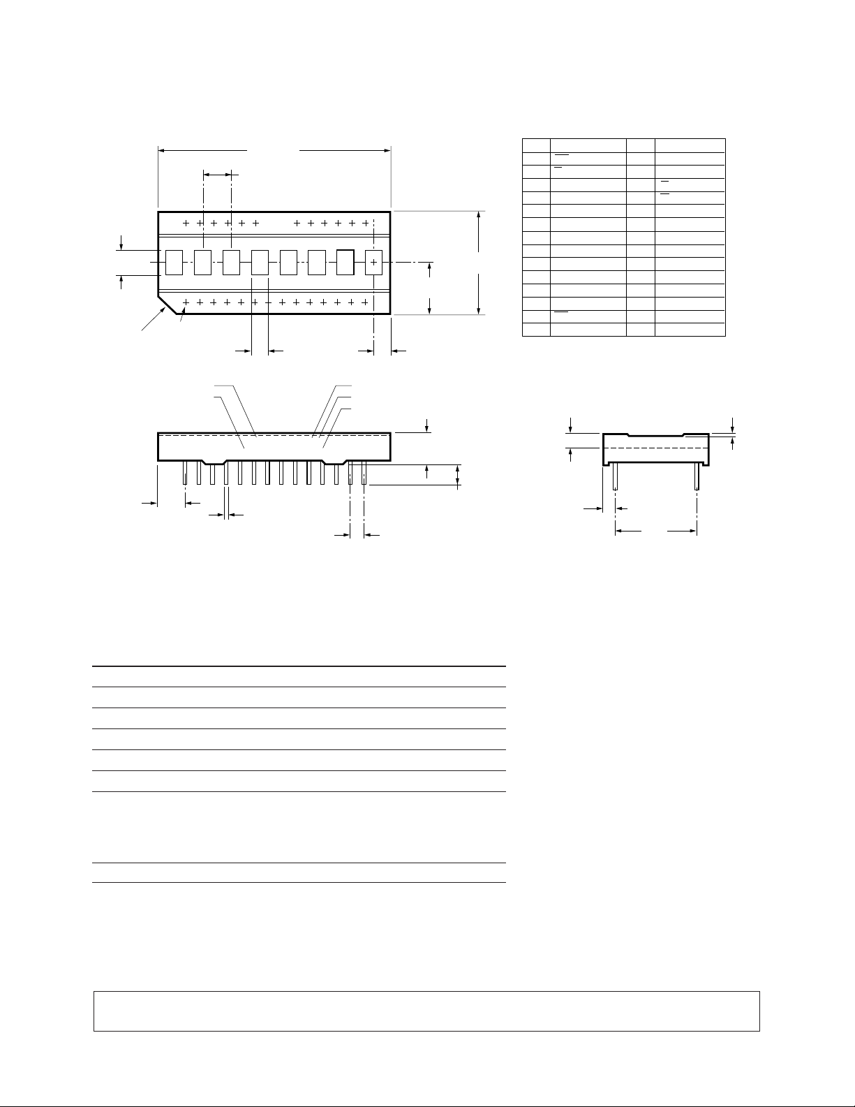
Package Dimensions
SYM.
TYP.
TYP. (NON-ACCUM)
LUMINOUS INTENSITY CATEGORY
COLOR BIN (NOTE 3)
COUNTRY OF ORIGIN
2.17
(0.085)
IMAGE PLANE
(FOR REFERENCE ONLY)
2.01 (0.08)
5.31
(0.209)
9.8
(0.386)
4.81
(0.189)
[4]
3.92
(0.154)
SYM.
4.79
(0.189)
2.54 ± 0.13
(0.100 ± 0.005)
TYP.
DIA.
0.51 ± 0.13
(0.020 ± 0.005)
PART NUMBER
15.24
(0.600)
0.25
(0.010)
PIN # FUNCTION PIN # FUNCTION
1
2
3
4
5
6
7
8
9
10
11
12
13
14
RST
FL
A
0
A
1
A
2
A
3
DO NOT CONNECT
DO NOT CONNECT
DO NOT CONNECT
A
4
CLS
CLK
WR
V
DD
15
16
17
18
19
20
21
22
23
24
25
26
27
28
GND (SUPPLY)
GND (LOGIC)
CE
RD
D
0
D
1
NO PIN
NO PIN
D
2
D
3
D
4
D
5
D
6
D
7
PIN FUNCTION ASSIGNMENT TABLE
3 4 5
6
7
19.58
(0.771)
2.69
(0.106)
42.59 (1.677)
TYP.
5.33
(0.210)
SYM.
2.64
(0.104)
PIN 1 IDENTIFIER
PIN DESIGNATION
NOTES:
1. DIMENSIONS ARE IN mm (INCHES).
2. UNLESS OTHERWISE SPECIFIED, TOLERANCE ON ALL DIMENSIONS IS ± 0.25 mm (0.010 INCH).
3. FOR YELLOW AND GREEN DEVICES ONLY.
HDSP-21XX Y Z
YYWW COO
DATE CODE
2
1
28
1
0
Absolute Maximum Ratings
Supply Voltage, VDD to Ground
Operating Voltage, VDD to Ground
Input Voltage, Any Pin to Ground -0.3 to VDD +0.3 V
Free Air Operating Temperature Range, T
Storage Temperature Range, TS -55°C to +100°C
Relative Humidity (non-condensing) 85%
Soldering Temperature
[1.59 mm (0.063 in.) Below Body]
Solder Dipping 260°C for 5 secs
Wave Soldering 250°C for 3 secs
ESD Protection @ 1.5 kΩ, 100 pF VZ = 4 kV (each pin)
Notes:
1. Maximum Voltage is with no LEDs illuminated.
2. 20 dots ON in all locations at full brightness.
3. Maximum supply voltage is 5.25 V for operation above 70°C.
ESD WARNING: STANDARD CMOS HANDLING PRECAUTIONS SHOULD BE OBSERVED TO AVOID STATIC DISCHARGE.
2
[1]
-0.3 to 7.0 V
[2]
5.5 V
[3]
-45°C to +85°C
A
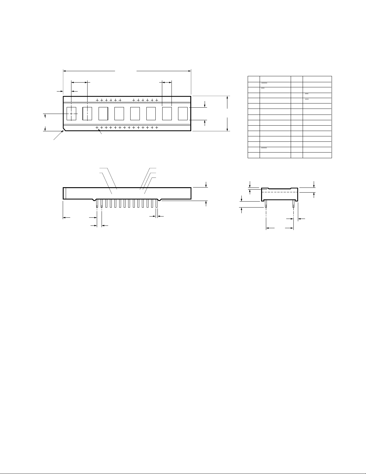
Package Dimensions
SYM.
TYP.
TYP. (NON-ACCUM)
LUMINOUS INTENSITY CATEGORY
COLOR BIN (NOTE 3)
COUNTRY OF ORIGIN
2.08
(0.082)
IMAGE PLANE
(FOR REFERENCE ONLY)
2.01 (0.79)
6.60
(0.260)
9.70
(0.382)
6.96
(0.274)
[4]
3.91
(0.154)
SYM.
19.01
(0.749)
2.54 ± 0.13
(0.100 ± 0.005)
TYP.
DIA.
0.51 ± 0.13
(0.200 ± 0.005)
PART NUMBER
15.24
(0.600)
0.38
(0.015)
PIN # FUNCTION PIN # FUNCTION
1
2
3
4
5
6
7
8
9
10
11
12
13
14
RST
FL
A
0
A
1
A
2
A
3
DO NOT CONNECT
DO NOT CONNECT
DO NOT CONNECT
A
4
CLS
CLK
WR
V
DD
15
16
17
18
19
20
21
22
23
24
25
26
27
28
GND (SUPPLY)
GND (LOGIC)
CE
RD
D
0
D
1
NO PIN
NO PIN
D
2
D
3
D
4
D
5
D
6
D
7
PIN FUNCTION ASSIGNMENT TABLE
3 4 5
6
7
19.41
(0.764)
4.51
(0.178)
70.87 (2.790)
TYP.
8.84
(0.348)
TYP.
PIN 1 IDENTIFIER
PIN DESIGNATION
NOTES:
1. DIMENSIONS ARE IN mm (INCHES).
2. UNLESS OTHERWISE SPECIFIED, TOLERANCE ON ALL DIMENSIONS IS ± 0.25 mm (0.010 INCH).
3. FOR YELLOW AND GREEN DEVICES ONLY.
HDSP-250X Y Z
YYWW COO
DATE CODE
2
1
1
28
0
TYP.
5.08
(0.200)
3
ASCII Character Set HDSP-210X, HDSP-211X, HDSP-250X Series
D7
D6
D5
D4
BITS
D3 D0D2 D1
ROW
COLUMN
0000 0
0001 1
0010 2
0011 3
0100 4
0101 5
0110 6
0111 7
1000 8
1001 9
1010 A
1011 B
1100 C
1101 D
1110 E
1111 F
0
0
0
0
0
0
0
0
1
1
0
0
1
0
2
0
0
1
1
3
0
1
0
0
4
0
1
0
1
5
0
1
1
0
6
0
1
1
1
7
1
X
X
X
8–F
16
U
S
E
R
D
E
F
I
N
E
D
C
H
A
R
A
C
T
E
R
S
Recommended Operating Conditions
Parameter Symbol Minimum Nominal Maximum Units
Supply Voltage VDD 4.5 5.0 5.5 V
4
Electrical Characteristics Over Operating Temperature Range (-45°C to +85°C)
4.5 V < VDD < 5.5 V, unless otherwise specied
TA = 25°C -45°C < TA < + 85°C
VDD = 5.0 4.5 V < VDD < 5.5 V
Parameter Symbol Typ. Max. Min. Max. Units Test Conditions
Input Leakage IIH 1.0 µA VIN = 0 to VDD,
(Input without pullup) IIL -1.0 pins CLK, D0-D
A0-A
Input Current I
-11 -18 -30 µA VIN = 0 to VDD,
IPL
(Input with pullup) pins CLS, RST,
WR, RD, CE, FL
IDD Blank I
(BLK) 0.5 3.0 4.0 mA VIN = V
DD
IDD 8 digits IDD(V) 200 255 330 mA “V” on in all 8
12 dots/character
[1,2]
locations
IDD 8 digits IDD(#) 300 370 430 mA “#” on in al
20 dots/character
[1,2,3,4]
Input Voltage High VIH 2.0 VDD V
+0.3
Input Voltage Low VIL GND 0.8 V
-0.3 V
Output Voltage High VOH 2.4 V VDD = 4.5 V,
IOH = -40 µA
Output Voltage Low VOL 0.4 V VDD = 4.5 V,
D0-D
7
Output Voltage Low VOL 0.4 V VDD = 4.5 V,
CLK IOL = 40 µA
High Level Output IOH -60 mA VDD = 5.0 V
Current
Low Level Output IOL 50 mA VDD = 5.0 V
Current
Thermal Resistance Rq
15 °C/W
J-C
IC Junction-to-Case
4
DD
locations
IOL = 1.6 mA
Notes:
1. Average IDD measured at full brightness. See Table 2 in Control Word Section for IDD at lower brightness levels. Peak IDD = 28/15 x IDD (#).
2. Maximum IDD occurs at -55°C.
3. Maximum IDD(#) = 355 mA at VDD = 5.25 V and IC TJ = 150°C.
4. Maximum IDD(#) = 375 mA at VDD = 5.5 V and IC TJ = 150°C.
5
 Loading...