

Page 1
HCPL-7710/0710
8
7
6
1
3
SHIELD
5
2
4
**V
DD1
V
I
NC*
GND
1
V
DD2
**
V
O
GND
2
VI, INPUT LED1
H
L
OFF
ON
TRUTH TABLE
(POSITIVE LOGIC)
NC*
I
O
LED1
VO, OUTPUT
H
L
VI, INPUT LED1
H
L
OFF
ON
TRUTH TABLE
(POSITIVE LOGIC)
VO, OUTPUT
H
L
Lead (Pb) Free
RoHS 6 fully
compliant
RoHS 6 fully compliant options available;
-xxxE denotes a lead-free product
40 ns Propagation Delay, CMOS Optocoupler
Data Sheet
Description
Available in either an 8-pin DIP or SO-8 package style
respectively, the HCPL-7710 or HCPL-0710 optocouplers
utilize the latest CMOS IC technology to achieve outstanding performance with very low power consumption. The
HCPL-x710 require only two bypass capacitors for complete
CMOS compatibility.
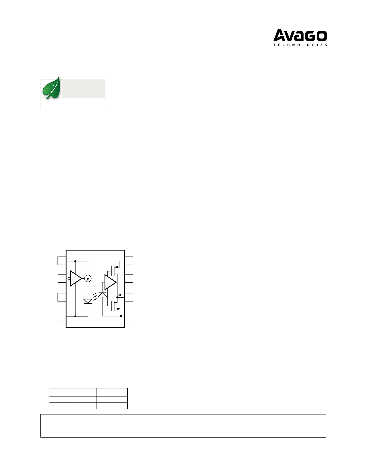
Basic building blocks of the HCPL-x710 are a CMOS LED
driver IC, a high speed LED and a CMOS detector IC. A
CMOS logic input signal controls the LED driver IC which
supplies current to the LED. The detector IC incorporates
an integrated photodiode, a high-speed transimpedance amplier, and a voltage comparator with an output
driver.
Functional Diagram
Features
• +5 V CMOS compatibility
• 8 ns maximum pulse width distortion
• 20 ns maximum prop. delay skew
• High speed: 12 Mbd
• 40 ns maximum prop. delay
• 10 kV/µs minimum common mode rejection
• -40°C to 100°C temperature range
• Safety and regulatory approvals
UL Recognized
3750 V rms for 1 min. per UL 1577
5000 V rms for 1 min. per UL 1577 (for HCPL-7710
option 020)
CSA Component Acceptance Notice #5
IEC/EN/DIN EN 60747-5-2
– V
– V
= 630 Vpeak for HCPL-7710 Option 060
IORM
= 560 Vpeak for HCPL-0710 Option 060
IORM
Applications
• Digital eldbus isolation: DeviceNet, SDS, Probus
• AC plasma display panel level shifting
• Multiplexed data transmission
• Computer peripheral interface
• Microprocessor system interface
* Pin 3 is the anode of the internal LED and must be left
unconnected for guaranteed data sheet performance.
Pin 7 is not connected internally.
** A 0.1 µF bypass capacitor must be connected
between pins 1 and 4, and 5 and 8.
CAUTION: It is advised that normal static precautions be taken in handling and assembly
of this component to prevent damage and/or degradation which may be induced by ESD.
Page 2

Selection Guide
8-Pin DIP Small Outline
(300 Mil) SO-8
HCPL-7710 HCPL-0710
Ordering Information
HCPL-0710 and HCPL-7710 are UL Recognized with 3750 Vrms for 1 minute per UL1577.
Option
Part
number
HCPL-7710
HCPL-0710
To order, choose a part number from the part number column and combine with the desired option from the option
column to form an order entry.
Example 1:
RoHS
Compliant
-000E No option
-300E #300 X X 50 per tube
-500E #500 X X X 1000 per reel
-020E -020 X 50 per tube
-320E -320 X X X 50 per tube
-520E -520 X X X X 1000 per reel
-060E #060 X 50 per tube
-360E #360 X X X 50 per tube
-560E #560 X X X X 1000 per reel
-000E No option
-500E #500 X X 1500 per reel
-060E #060 X X 100 per tube
-560E #560 X X X 1500 per reel
Non RoHS
Compliant
Package
300mil
DIP-8
SO-8
Surface
Mount
X 100 per tube
Gull
Wing
Tape
& Reel
UL 5000
Vrms/ 1
Minute rating
IEC/EN/DIN
EN 60747-5-2 Quantity
50 per tube
HCPL-7710-560E to order product of Gull Wing Surface Mount package in Tape and Reel packaging with IEC/EN/
DIN EN 60747-5-2 Safety Approval in RoHS compliant.
Example 2:
HCPL-0710 to order product of Small Outline SO-8 package in tube packaging and non RoHS compliant.
Option datasheets are available. Contact your Avago sales representative or authorized distributor for information.
Remarks: The notation ‘#XXX’ is used for existing products, while (new) products launched since 15th July 2001 and
RoHS compliant option will use ‘-XXXE‘.
2
Page 3
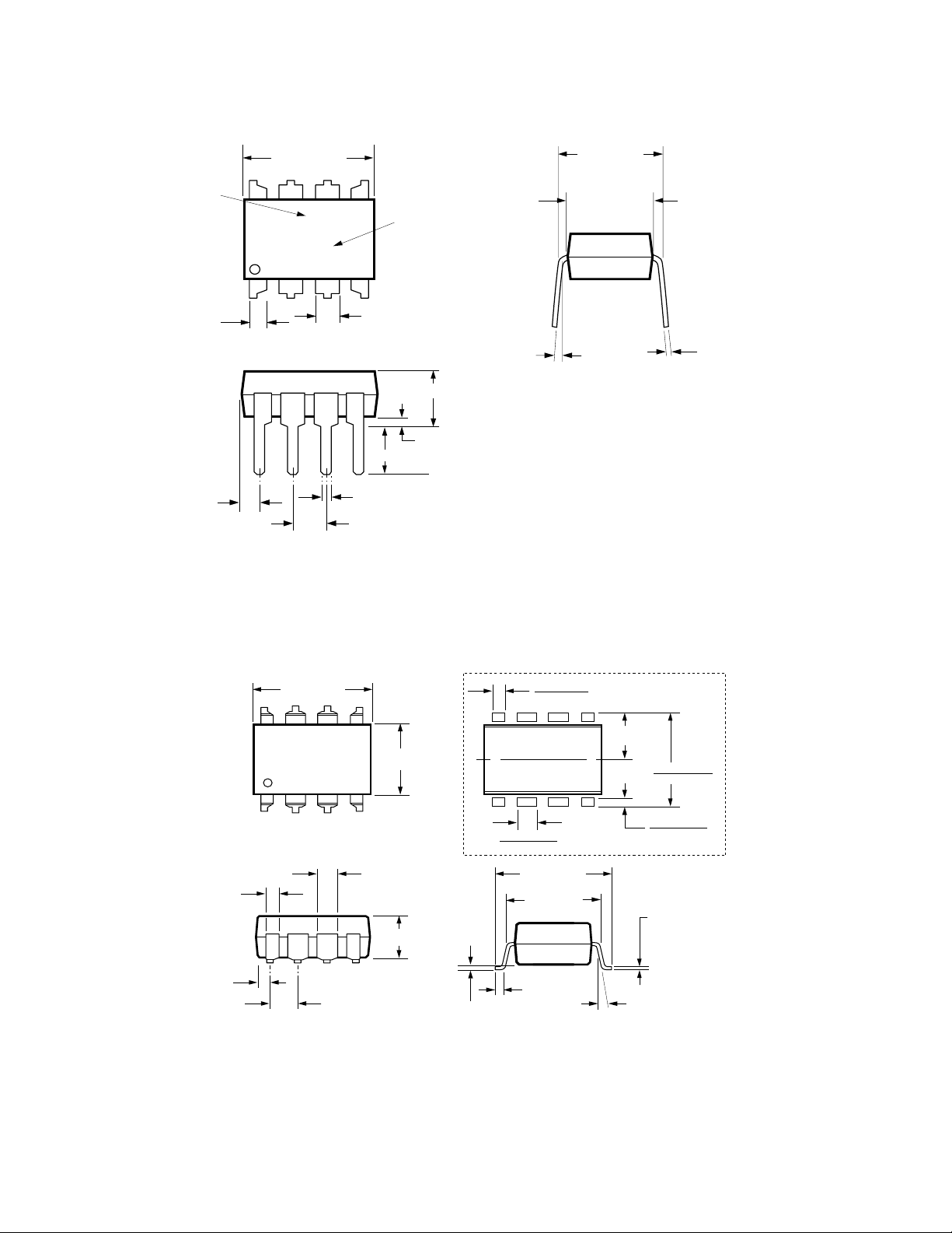
Package Outline Drawing
9.65 ± 0.25
(0.380 ± 0.010)
1.78 (0.070) MAX.
1.19 (0.047) MAX.
A XXXX
YYWW
DATE CODE
1.080 ± 0.320
(0.043 ± 0.013)
2.54 ± 0.25
(0.100 ± 0.010)
0.51 (0.020) MIN.
0.65 (0.025) MAX.
4.70 (0.185) MAX.
2.92 (0.115) MIN.
DIMENSIONS IN MILLIMETERS AND (INCHES).
5678
4321
5° TYP.
0.254
+ 0.076
- 0.051
(0.010
+ 0.003)
- 0.002)
7.62 ± 0.25
(0.300 ± 0.010)
6.35 ± 0.25
(0.250 ± 0.010)
TYPE NUMBER
*MARKING CODE LETTER FOR OPTION NUMBERS
"L" = OPTION 020
"V" = OPTION 060
OPTION NUMBERS 300 AND 500 NOT MARKED.
0.635 ± 0.25
(0.025 ± 0.010)
12° NOM.
9.65 ± 0.25
(0.380 ± 0.010)
0.635 ± 0.130
(0.025 ± 0.005)
7.62 ± 0.25
(0.300 ± 0.010)
Outline (8-pin DIP - Option 300)
5
6
7
8
4
3
2
1
9.65 ± 0.25
(0.380 ± 0.010)
6.350 ± 0.25
(0.250 ± 0.010)
1.016 (0.040)
1.194 (0.047)
1.194 (0.047)
1.778 (0.070)
9.398 (0.370)
9.906 (0.390)
4.826
(0.190)
TYP.
0.381 (0.015)
0.635 (0.025)
PAD LOCATION (FOR REFERENCE ONLY)
1.080 ± 0.320
(0.043 ± 0.013)
4.19
(0.165)
MAX.
1.780
(0.070)
MAX.
1.19
(0.047)
MAX.
2.54
(0.100)
BSC
DIMENSIONS IN MILLIMETERS (INCHES).
LEAD COPLANARITY = 0.10 mm (0.004 INCHES).
0.254
+ 0.076
- 0.051
(0.010
+ 0.003)
- 0.002)
HCPL-7710 8-Pin DIP Package
Package Outline Drawing
HCPL-7710 Package with Gull Wing Surface Mount Option 300
3
Page 4
Package Outline Drawing
XXXV
YWW
8 7 6 5
4321
5.994 ± 0.203
(0.236 ± 0.008)
3.937 ± 0.127
(0.155 ± 0.005)
0.406 ± 0.076
(0.016 ± 0.003)
1.270
(0.050)
BSC
5.080 ± 0.127
(0.200 ± 0.005)
3.175 ± 0.127
(0.125 ± 0.005)
1.524
(0.060)
45° X
0.432
(0.017)
0.228 ± 0.025
(0.009 ± 0.001)
TYPE NUMBER
(LAST 3 DIGITS)
DATE CODE
0.305
(0.012)
MIN.
TOTAL PACKAGE LENGTH (INCLUSIVE OF MOLD FLASH)
5.207 ± 0.254 (0.205 ± 0.010)
DIMENSIONS IN MILLIMETERS (INCHES).
LEAD COPLANARITY = 0.10 mm (0.004 INCHES) MAX.
OPTION NUMBER 500 NOT MARKED.
NOTE: FLOATING LEAD PROTRUSION IS 0.15 mm (6 mils) MAX.
0.203 ± 0.102
(0.008 ± 0.004)
7°
PIN ONE
0 ~ 7°
*
*
7.49 (0.295)
1.9 (0.075)
0.64 (0.025)
LAND PATTERN RECOMMENDATION
0
TIME (SECONDS)
TEMPERATURE ( °C)
200
100
50 150100 200 250
300
0
30
SEC.
50 SEC.
30
SEC.
160°C
140°C
150°C
PEAK
TEMP.
245°C
PEAK
TEMP.
240°C
PEAK
TEMP.
230°C
SOLDERING
TIME
200°C
PREHEATING TIME
150°C, 90 + 30 SEC.
2.5°C ± 0.5°C/SEC.
3°C + 1°C/- 0.5°C
TIGHT
TYPICAL
LOOSE
ROOM
TEMPERATURE
PREHEATING RATE 3°C + 1°C/- 0.5°C/SEC.
REFLOW HEATING RATE 2.5°C ± 0.5°C/SEC.
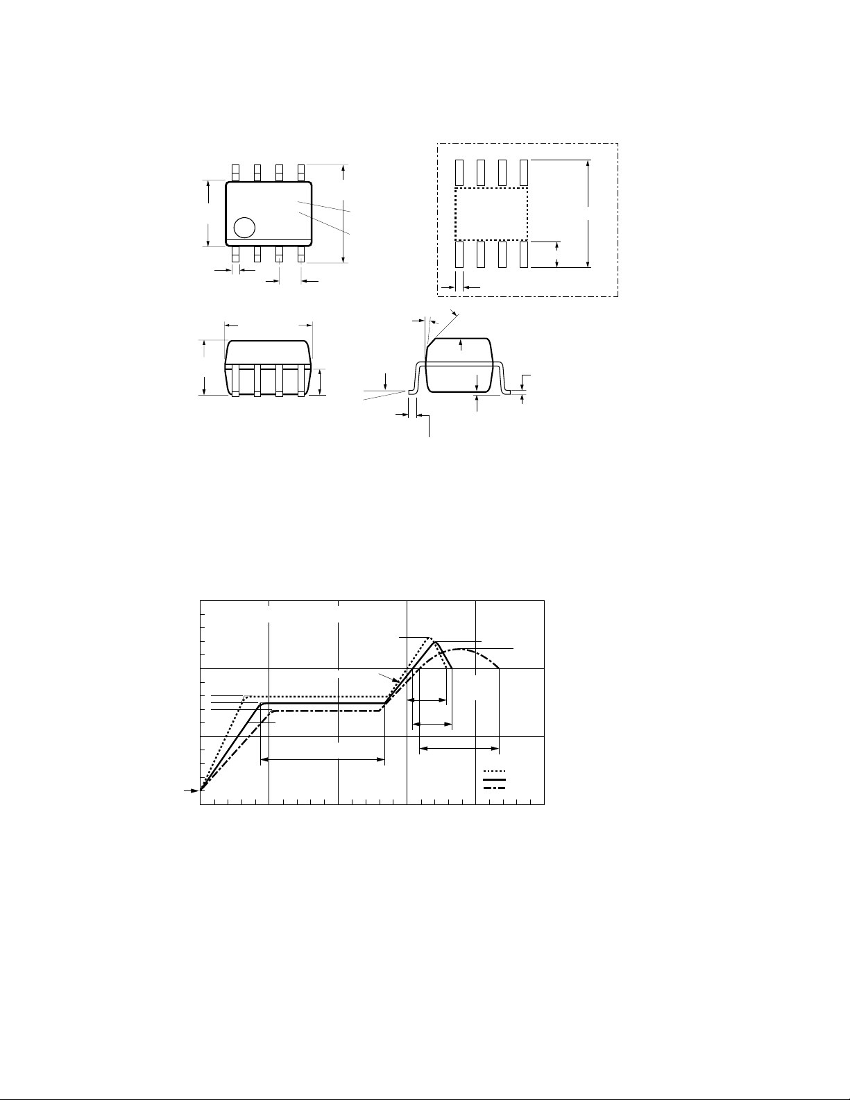
HCPL-0710 Outline Drawing (Small Outline SO-8 Package)
Solder Reow Thermal Prole
4
Note: Non-halide ux should be used.
Page 5
Recommended Pb-Free IR Prole
217 °C
RAMP-DOWN
6 °C/SEC. MAX.
RAMP-UP
3 °C/SEC. MAX.
150 - 200 °C
260 +0/-5 °C
t 25 °C to PEAK
60 to 150 SEC.
20-40 SEC.
TIME WITHIN 5 °C of ACTUAL
PEAK TEMPERATURE
t
p
t
s
PREHEAT
60 to 180 SEC.
t
L
T
L
T
smax
T
smin
25
T
p
TIME
TEMPERATURE
NOTES:
THE TIME FROM 25 °C to PEAK TEMPERATURE = 8 MINUTES MAX.
T
smax
= 200 °C, T
smin
= 150 °C
Note: Non-halide ux should be used.
Regulatory Information
The HCPL-x710 have been approved by the following organizations:
UL
Recognized under UL 1577, component recognition
program, File E55361.
IEC/EN/DIN EN 60747-5-2
Approved under:
IEC 60747-5-2:1997 + A1:2002
EN 60747-5-2:2001 + A1:2002
CSA
Approved under CSA Component Acceptance Notice
#5, File CA 88324.
DIN EN 60747-5-2 (VDE 0884
Teil 2):2003-01.
(Option 060 only)
Insulation and Safety Related Specications
Value
Parameter Symbol 7710 0710 Units Conditions
Minimum External Air L(I01) 7.1 4.9 mm Measured from input terminals to output
Gap (Clearance) terminals, shortest distance through air.
Minimum External L(I02) 7.4 4.8 mm Measured from input terminals to output
Tracking (Creepage) terminals, shortest distance path along body.
Minimum Internal Plastic 0.08 0.08 mm Insulation thickness between emitter and
Gap (Internal Clearance) detector; also known as distance through
insulation.
Tracking Resistance CTI ≥175 ≥175 Volts DIN IEC 112/VDE 0303 Part 1
(Comparative Tracking Index)
Isolation Group IIIa IIIa Material Group (DIN VDE 0110, 1/89, Table 1)
All Avago data sheets report the creepage and clearance
inherent to the optocoupler component itself. These
dimensions are needed as a starting point for the equipment designer when determining the circuit insulation
requirements. However, once mounted on a printed circuit
board, minimum creepage and clearance requirements
must be met as specied for individual equipment standards. For creepage, the shortest distance path along the
5
surface of a printed circuit board between the solder llets
of the input and output leads must be considered. There
are recommended techniques such as grooves and ribs
which may be used on a printed circuit board to achieve
desired creepage and clearances. Creepage and clearance
distances will also change depending on factors such as
pollution degree and insulation level.
Page 6

IEC/EN/DIN EN 60747-5-2 Insulation Related Characteristics (Option 060)
HCPL-7710 HCPL-0710
Description Symbol Option 060 Option 060 Units
Installation classication per DIN VDE 0110/1.89, Table 1
for rated mains voltage ≤150 V rms I-IV I-IV
for rated mains voltage ≤300 V rms I-IV I-III
for rated mains voltage ≤450 V rms I-III
Climatic Classication 55/100/21 55/100/21
Pollution Degree (DIN VDE 0110/1.89) 2 2
Maximum Working Insulation Voltage V
630 560 V peak
IORM
Input to Output Test Voltage, Method b† VPR 1181 1050 V peak
V
x 1.875 = VPR, 100% Production
IORM
Test with tm = 1 sec, Partial Discharge < 5 pC
Input to Output Test Voltage, Method a† VPR 945 840 V peak
V
x 1.5 = VPR, Type and Sample Test,
IORM
tm = 60 sec, Partial Discharge < 5 pC
Highest Allowable Overvoltage† V
(Transient Overvoltage, t
= 10 sec)
ini
6000 4000 V peak
IOTM
Safety Limiting Values
(Maximum values allowed in the event of a failure,
also see Thermal Derating curve, Figure 11.)
Case Temperature TS 175 150 °C
Input Current I
Output Power P
Insulation Resistance at TS, V10 = 500 V RIO ≥10
230 150 mA
S,INPUT
600 600 mW
S,OUTPUT
9
≥109 Ω
†Refer to the front of the optocoupler section of the Isolation and Control Component Designer’s Catalog, under Product Safety Regulations section IEC/EN/DIN EN 60747-5-2, for a detailed description.
Note: These optocouplers are suitable for “safe electrical isolation” only within the safety limit data. Maintenance of the safety data shall be
ensured by means of protective circuits.
Note: The surface mount classication is Class A in accordance with CECC 00802.
Absolute Maximum Ratings
Parameter Symbol Min. Max. Units
Storage Temperature TS –55 125 °C
Ambient Operating Temperature TA –40 +100 °C
Supply Voltages V
Input Voltage VI –0.5 V
Output Voltage VO –0.5 V
DD1
, V
0 6.0 Volts
DD2
+0.5 Volts
DD1
+0.5 Volts
DD2
Input Current II –10 +10 mA
Average Output Current IO 10 mA
Lead Solder Temperature 260°C for 10 sec., 1.6 mm below seating plane
Solder Reow Temperature Prole See Solder Reow Temperature Prole Section
Recommended Operating Conditions
Parameter Symbol Min. Max. Units
Ambient Operating Temperature TA –40 +100 °C
Supply Voltages V
Logic High Input Voltage VIH 2.0 V
DD1
, V
4.5 5.5 V
DD2
DD1
V
Logic Low Input Voltage VIL 0.0 0.8 V
Input Signal Rise and Fall Times tr, tf 1.0 ms
6
Page 7

Electrical Specications
Test conditions that are not specied can be anywhere within the recommended operating range.
All typical specications are at TA = +25°C, V
DD1
= V
DD2
= +5 V.
DC Specications
Parameter Symbol Min. Typ. Max. Units Test Conditions
Logic Low Input I
Supply Current
[1]
Logic High Input I
Supply Current
Input Supply Current I
Output Supply Current I
6.0 10.0 mA VI = 0 V
DD1L
1.5 3.0 mA VI = V
DD1H
13.0 mA
DD1
5.5 11.0 mA
DD2
DDI
Input Current II -10 10 µA
Logic High Output VOH 4.4 5.0 V IO = -20 µA, VI = V
Voltage 4.0 4.8 IO = -4 mA, VI = V
Logic Low Output VOL 0 0.1 V IO = -20 µA, VI = V
Voltage 0.5 1.0 IO = -4 mA, VI = V
IH
IH
IL
IL
Switching Specications
Parameter Symbol Min. Typ. Max. Units Test Conditions
Propagation Delay Time t
to Logic Low Output
[2]
CMOS Signal Levels
Propagation Delay Time t
to Logic Low Output
[2]
CMOS Signal Levels
Propagation Delay Time t
20 40 ns CL = 15 pF
PHL
20 40 ns CL = 15 pF
PHL
23 40 ns CL = 15 pF
PLH
to Logic High Output CMOS Signal Levels
Pulse Width
[3]
PW 80 ns CL = 15 pF
CMOS Signal Levels
Data Rate
[3]
12.5 MBd CL = 15 pF
CMOS Signal Levels
Pulse Width Distortion
|t
- t
PHL
| CMOS Signal Levels
PLH
Propagation Delay Skew
[4]
PWD 3 8 ns CL = 15 pF
[5]
t
20 ns CL = 15 pF
PSK
Output Rise Time tR 9 ns CL = 15 pF
(10 - 90%) CMOS Signal Levels
Output Fall Time tF 8 ns CL = 15 pF
(90 - 10%) CMOS Signal Levels
Common Mode |CMH| 10 20 kV/µs VI = V
Transient Immunity at 0.8 V
Logic High Output
[6]
VCM = 1000 V
DD1
DD1
, VO >
,
Common Mode |CML| 10 20 kV/µs VI = 0 V, VO > 0.8 V,
Transient Immunity at VCM = 1000 V
Logic Low Output
Input Dynamic Power C
Dissipation Capacitance
Output Dynamic Power C
Dissipation Capacitance
[6]
60 pF
[7]
[7]
PD1
10 pF
PD2
7
Page 8

V
O
(V)
0
0
VI (V)
5
4
1
41 2 3
5
3
2
0 °C
25 °C
85 °C
V
ITH
(V)
4.5
1.6
V
DD1
(V)
5.5
2.1
1.7
5.254.75 5
2.2
2.0
1.8
1.9
0 °C
25 °C
85 °C
T
PLH
, T
PHL
(ns)
0
15
TA (C)
80
27
17
6020 30
29
25
19
21
10 40 50 70
23
T
PLH
T
PHL
Package Characteristics
Parameter Symbol Min. Typ. Max. Units Test Conditions
Input-Output Momentary
Withstand Voltage
[8, 9, 10]
Resistance
(Input-Output)
[8]
Capacitance
(Input-Output)
Input Capacitance
[8]
[11]
Input IC Junction-to-Case
Thermal Resistance
Output IC Junction-to-Case
Thermal Resistance
Package Power Dissipation P
Notes:
1. The LED is ON when VI is low and OFF when VI is high.
2. t
propagation delay is measured from the 50% level on the falling edge of the VI signal to the 50% level of the falling edge of the VO signal.
PHL
t
propagation delay is measured from the 50% level on the rising edge of the VI signal to the 50% level of the rising edge of the VO signal.
PLH
3. Mimimum Pulse Width is the shortest pulse width at which 10% maximum, Pulse Width Distortion can be guaranteed. Maximum Data Rate is
the inverse of Minimum Pulse Width. Operating the HCPL-x710 at data rates above 12.5 MBd is possible provided PWD and data dependent
jitter increases and relaxed noise margins are tolerable within the application. For instance, if the maximum allowable variation of bit width is
30%, the maximum data rate becomes 37.5 MBd. Please note that HCPL-x710 performances above 12.5 MBd are not guaranteed by HewlettPackard.
4. PWD is dened as |t
5. t
is equal to the magnitude of the worst case dierence in t
PSK
the recommended operating conditions.
6. CMH is the maximum common mode voltage slew rate that can be sustained while maintaining VO > 0.8 V
mode voltage slew rate that can be sustained while maintaining VO < 0.8 V. The common mode voltage slew rates apply to both rising and
falling common mode voltage edges.
7. Unloaded dynamic power dissipation is calculated as follows: CPD * V
8. Device considered a two-terminal device: pins 1, 2, 3, and 4 shorted together and pins 5, 6, 7, and 8 shorted together.
9. In accordance with UL1577, each HCPL-0710 is proof tested by applying an insulation test voltage ≥4500 V
tion current limit, I
tion current limit, I
10. The Input-Output Momentary Withstand Voltage is a dielectric voltage rating that should not be interpreted as an input-output continuous
voltage rating. For the continuous voltage rating refer to your equipment level safety specication or Avago Application Note 1074 entitled
“Optocoupler Input-Output Endurance Voltage.”
11. CI is the capacitance measured at pin 2 (VI).
- t
|. %PWD (percent pulse width distortion) is equal to the PWD divided by pulse width.
PHL
PLH
≤5 µA). Each HCPL-7710 is proof tested by applying an insulation test voltage ≥ 4500 V rms for 1 second (leakage detec-
I-O
≤ 5 µA).
I-O
0710 V
3750 Vrms RH = 50%,
ISO
7710 3750
Option 020 5000
-7710
R
I-O
C
I-O
C
I
q
jci
10
0.6 pF f = 1 MHz
3.0
145 °C/W Thermocouple
-0710 160
-7710
q
jco
140
-0710 135
PD
and/or t
PHL
that will be seen between units at any given temperature within
PLH
* f + IDD * VDD, where f is switching frequency in MHz.
DD2
12
W
150 mW
t = 1 min.,
TA = 25°C
V
= 500 Vdc
I-O
located at center
underside of package
. CML is the maximum common
DD2
for 1 second (leakage detec-
RMS
Figure 1. Typical output voltage vs. input voltage. Figure 2. Typical input voltage switching threshold vs.
input supply voltage.
8
Figure 3. Typical propagation delays vs. temperature.
Page 9

PWD
(ns)
0
0
TA (C)
80
3
6020
4
1
40
2
T
R
(ns)
0
12
TA (C)
80
14
6020
15
13
40
T
F
(ns)
0
2
TA (C)
80
6
6020
7
3
40
5
4
T
R
(ns)
0
5
CI (pF)
35
23
25
25
9
15
15
105 20 30
11
19
21
17
13
7
FALL TIME
(ns)
0
0
CI (pF)
35
9
25
10
2
15
5
105 20 30
3
7
8
6
4
1
Figure 4. Typical pulse width distortion vs. tempera-
T
PLH
, T
PHL
(ns)
15
15
CI (pF)
50
27
40
29
17
30
23
21
2520 35 45
19
25
T
PLH
T
PHL
PWD
(ns)
15
0
CI (pF)
50
5
40
6
1
30
3
2520 35 45
2
4
OUTPUT POWER - P
S
, INPUT CURRENT - I
S
0
0
TA - CASE TEMPERATURE - oC
20050
400
12525 75 100 150
600
800
200
100
300
500
700
175
(230)
PS (mW)
I
S
(mA)
STANDARD 8 PIN DIP PRODUCT
OUTPUT POWER - P
S
, INPUT CURRENT - I
S
0
0
TA - CASE TEMPERATURE - oC
20050
400
12525 75 100 150
600
800
200
100
300
500
700
175
(150)
PS (mW)
IS (mA)
SURFACE MOUNT SO8 PRODUCT
ture.
Figure 5. Typical rise time vs. temperature. Figure 6. Typical fall time vs. temperature.
Figure 7. Typical propagation delays vs. output load
capacitance.
Figure 10. Typical fall time vs. load capacitance.
9
Figure 8. Typical pulse width distortion vs. output load
capacitance.
Figure 11. Thermal derating curve, dependence of Safety Limiting Value with case temperature per IEC/EN/DIN EN
60747-5-2.
Figure 9. Typical rise time vs. load capacitance.
Page 10

Application Information
INPUT
t
PLH
t
PHL
OUTPUT
V
I
V
O
10%
90%90%
10%
V
OH
V
OL
0 V
50%
5 V CMOS
2.5 V CMOS
V
DD2
C1 C2
710
YYWW
V
O
GND
2
V
DD1
V
I
GND
1
C1, C2 = 0.01 µF TO 0.1 µF
7
5
6
8
2
3
4
1
GND
2
C1 C2
NC
V
DD2
NC
V
O
V
DD1
V
I
710
YYWW
C1, C2 = 0.01 µF TO 0.1 µF
GND
1
Bypassing and PC Board Layout
The HCPL-x710 optocouplers are extremely easy to
use. No external interface circuitry is required because
the HCPL-x710 use high-speed CMOS IC technology
allowing CMOS logic to be connected directly to the
inputs and outputs.
As shown in Figure 12, the only external components
Figure 12. Recommended Printed Circuit Board layout.
required for proper operation are two bypass capacitors.
Capacitor values should be between 0.01 µF and 0.1 µF.
For each capacitor, the total lead length between both
ends of the capacitor and the power-supply pins should
not exceed 20 mm. Figure 13 illustrates the recommended printed circuit board layout for the HPCL-x710.
Figure 13. Recommended Printed Circuit Board layout.
Propagation Delay, Pulse-Width Distortion and Propagation Delay
Skew
Propagation Delay is a gure of merit which describes
how quickly a logic signal propagates through a
system. The propagation delay from low to high (t
is the amount of time required for an input signal to
propagate to the output, causing the output to change
Figure 14.
10
from low to high. Similarly, the propagation delay from
high to low (t
)
PLH
input signal to propagate to the output, causing the
output to change from high to low. See Figure 14.
) is the amount of time required for the
PHL
Page 11

Pulse-width distortion (PWD) is the dierence between
50%
50%
t
PSK
V
I
V
O
V
I
V
O
2.5 V,
CMOS
2.5 V,
CMOS
DATA
INPUTS
CLOCK
DATA
OUTPUTS
CLOCK
t
PSK
t
PSK
t
PHL
and t
and often determines the maximum data
PLH
rate capability of a transmission system. PWD can be
expressed in percent by dividing the PWD (in ns) by
the minimum pulse width (in ns) being transmitted.
Typically, PWD on the order of 20 - 30% of the minimum
pulse width is tolerable. The PWD specication for the
HCPL-x710 is 8 ns (10%) maximum across recommended operating conditions. 10% maximum is dictated
by the most stringent of the three eldbus standards,
PROFIBUS.
Propagation delay skew, t
, is an important parameter
PSK
to consider in parallel data applications where synchronization of signals on parallel data lines is a concern. If
the parallel data is being sent through a group of optocouplers, dierences in propagation delays will cause
the data to arrive at the outputs of the optocouplers at
dierent times. If this dierence in propagation delay
is large enough it will determine the maximum rate at
which parallel data can be sent through the optocouplers.
Propagation delay skew is dened as the dierence between the minimum and maximum propagation delays, either t
PLH
or t
, for any given group
PHL
of optocouplers which are operating under the same
conditions (i.e., the same drive current, supply voltage,
output load, and operating temperature). As illustrated
in Figure 15, if the inputs of a group of optocouplers
are switched either ON or OFF at the same time, t
PSK
is
the dierence between the shortest propagation delay,
either t
either t
As mentioned earlier, t
PLH
PLH
or t
or t
, and the longest propagation delay,
PHL
.
PHL
can determine the maximum
PSK
parallel data transmission rate. Figure 16 is the timing
diagram of a typical parallel data application with both
the clock and data lines being sent through the optocouplers. The gure shows data and clock signals at the
inputs and outputs of the optocouplers. In this case the
data is assumed to be clocked o of the rising edge of
the clock.
Figure 15. Propagation delay skew waveform. Figure 16. Parallel data transmission example.
Propagation delay skew represents the uncertainty of
where an edge might be after being sent through an
optocoupler. Figure 16 shows that there will be uncertainty in both the data and clock lines. It is important
that these two areas of uncertainty not overlap,
otherwise the clock signal might arrive before all of
the data outputs have settled, or some of the data
outputs may start to change before the clock signal
has arrived. From these considerations, the absolute
tocouplers in a parallel application is twice t
A cautious design should use a slightly longer pulse
width to ensure that any additional uncertainty in the
rest of the circuit does not cause a problem.
The HCPL-x710 optocouplers oer the advantage of
guaranteed specications for propagation delays, pulsewidth distortion, and propagation delay skew over the
recommended temperature and power supply ranges.
minimum pulse width that can be sent through op-
11
PSK
.
Page 12

Digital Field Bus Communication Networks
CONTROLLER
TRANSCEIVER
OPTICAL
ISOLATION
BUS
INTERFACE
TRANSCEIVER
OPTICAL
ISOLATION
BUS
INTERFACE
TRANSCEIVER
OPTICAL
ISOLATION
BUS
INTERFACE
TRANSCEIVER
OPTICAL
ISOLATION
BUS
INTERFACE
TRANSCEIVER
OPTICAL
ISOLATION
BUS
INTERFACE
FIELD BUS
XXXXXX
YYY
SENSOR
DEVICE
CONFIGURATION
MOTOR
STARTER
MOTOR
CONTROLLER
To date, despite its many drawbacks, the 4 - 20 mA
analog current loop has been the most widely accepted
standard for implementing process control systems.
In today’s manufacturing environment, however,
automated systems are expected to help manage
the process, not merely monitor it. With the advent
of digital eld bus communication networks such as
DeviceNet, PROFIBUS, and Smart Distributed Systems
(SDS), gone are the days of constrained information.
Controllers can now receive multiple readings from eld
devices (sensors, actuators, etc.) in addition to diagnostic information.
The physical model for each of these digital eld bus
communication networks is very similar as shown in
Figure 17. Each includes one or more buses, an interface
unit, optical isolation, transceiver, and sensing and/or
actuating devices.
Figure 17. Typical eld bus communication physical model.
Optical Isolation for Field Bus Networks
To recognize the full benets of these networks, each
recommends providing galvanic isolation using Avago
optocouplers. Since network communication is bi-directional (involving receiving data from and transmitting
data onto the network), two Avago optocouplers are
needed. By providing galvanic isolation, data integrity is
retained via noise reduction and the elimination of false
signals. In addition, the network receives maximum protection from power system faults and ground loops.
Within an isolated node, such as the DeviceNet Node
shown in Figure 18, some of the node’s components are
referenced to a ground other than V- of the network.
12
These components could include such things as devices
with serial ports, parallel ports, RS232 and RS485 type
ports. As shown in Figure 18, power from the network is
used only for the transceiver and input (network) side of
the optocouplers.
Isolation of nodes connected to any of the three types of
digital eld bus networks is best achieved by using the
HCPL-x710 optocouplers. For each network, the HCPLx710 satisify the critical propagation delay and pulse
width distortion requirements over the temperature
range of 0°C to +85°C, and power supply voltage range
of 4.5 V to 5.5 V.
Page 13

Figure 18. Typical DeviceNet node.
NODE/APP SPECIFIC
uP/CAN
HCPL
x710
HCPL
x710
TRANSCEIVER
LOCAL
NODE
SUPPLY
5 V REG.
NETWORK
POWER
SUPPLY
V+ (SIGNAL)
V– (SIGNAL)
V+ (POWER)
V– (POWER)
GALVANIC
ISOLATION
BOUNDARY
AC LINE
DRAIN/SHIELD
SIGNAL
POWER
NODE/APP SPECIFIC
uP/CAN
HCPL
x710
HCPL
x710
TRANSCEIVER
REG.
V+ (SIGNAL)
V– (SIGNAL)
V+ (POWER)
V– (POWER)
GALVANIC
ISOLATION
BOUNDARY
DRAIN/SHIELD
SIGNAL
POWER
ISOLATED
SWITCHING
POWER
SUPPLY
NETWORK
POWER
SUPPLY
Implementing DeviceNet and SDS with the HCPL-x710
With transmission rates up to 1 Mbit/s, both DeviceNet
and SDS are based upon the same broadcast-oriented,
communications protocol — the Controller Area
Network (CAN). Three types of isolated nodes are recommended for use on these networks: Isolated Node
Powered by the Network (Figure 19), Isolated Node
with Transceiver Powered by the Network (Figure 20),
and Isolated Node Providing Power to the Network
(Figure 21).
Isolated Node Powered by the Network
This type of node is very exible and as can be seen in
Figure 19, is regarded as “isolated” because not all of its
components have the same ground reference. Yet, all
components are still powered by the network. This node
contains two regulators: one is isolated and powers the
CAN controller, node-specic application and isolated
(node) side of the two optocouplers while the other is
non-isolated. The non-isolated regulator supplies the
transceiver and the non-isolated (network) half of the
two optocouplers.
Figure 19. Isolated node powered by the network.
13
Page 14

Isolated Node with Transceiver Powered by the Network
NODE/APP SPECIFIC
uP/CAN
HCPL
0710
HCPL
0710
TRANSCEIVER
NON ISO
5 V
REG.
NETWORK
POWER
SUPPLY
V+ (SIGNAL)
V– (SIGNAL)
V+ (POWER)
V– (POWER)
GALVANIC
ISOLATION
BOUNDARY
AC LINE
DRAIN/SHIELD
SIGNAL
POWER
HCPL
0710
* OPTIONAL FOR BUS V + SENSE
Figure 20 shows a node powered by both the network
and another source. In this case, the transceiver and
isolated (network) side of the two optocouplers are
powered by the network. The rest of the node is
powered by the AC line which is very benecial when
an application requires a signicant amount of power.
This method is also desirable as it does not heavily load
the network.
More importantly, the unique “dual-inverting” design
of the HCPL-x710 ensure the network will not “lock-up”
if either AC line power to the node is lost or the node
powered-o. Specically, when input power (V
DD1
) to
the HCPL-x710 located in the transmit path is eliminated, a RECESSIVE bus state is ensured as the HCPL-x710
output voltage (VO) go HIGH.
*Bus V+ Sensing
It is suggested that the Bus V+ sense block shown in
Figure 20 be implemented. A locally powered node with
an un-powered isolated Physical Layer will accumulate
errors and become bus-o if it attempts to transmit. The
Bus V+ sense signal would be used to change the BOI
attribute of the DeviceNet Object to the “auto-reset”
(01) value. Refer to Volume 1, Section 5.5.3. This would
cause the node to continually reset until bus power was
detected. Once power was detected, the BOI attribute
would be returned to the “hold in bus-o” (00) value.
The BOI attribute should not be left in the “auto-reset”
(01) value since this defeats the jabber protection capability of the CAN error connement. Any inexpensive
low frequency optical isolator can be used to implement
this feature.
Figure 20. Isolated node with transceiver powered by the network.
14
Page 15

Isolated Node Providing Power to the Network
NODE/APP SPECIFIC
uP/CAN
HCPL
0710
HCPL
0710
TRANSCEIVER
5 V REG.
V+ (SIGNAL)
V– (SIGNAL)
V+ (POWER)
V– (POWER)
GALVANIC
ISOLATION
BOUNDARY
AC LINE
DRAIN/SHIELD
SIGNAL
POWER
ISOLATED
SWITCHING
POWER
SUPPLY
5 V REG.
DEVICENET NODE
Figure 21 shows a node providing power to the
network. The AC line powers a regulator which provides
ve (5) volts locally. The AC line also powers a 24 volt
isolated supply, which powers the network, and another
ve-volt regulator, which, in turn, powers the transceiver and isolated (network) side of the two optocouplers.
This method is recommended when there are a limited
number of devices on the network that don’t require
much power, thus eliminating the need for separate
power supplies.
More importantly, the unique “dual-inverting” design
of the HCPL-x710 ensure the network will not “lock-up”
if either AC line power to the node is lost or the node
powered-o. Specically, when input power (V
DD1
) to
the HCPL-x710 located in the transmit path is eliminated, a RECESSIVE bus state is ensured as the HCPL-x710
output voltage (VO) go HIGH.
Figure 21. Isolated node providing power to the network.
15
Page 16

Power Supplies and Bypassing
PROFIBUS USER:
CONTROL STATION
(CENTRAL PROCESSING)
OR FIELD DEVICE
USER INTERFACE
FDL/APP
PROCESSOR
TRANSCEIVER
OPTICAL ISOLATION
UART
PBC
MEDIUM
8
7
6
1
3
5
2
4
V
DD1
V
IN
GND
1
V
DD2
V
O
GND
2
HCPL-0710
4
3
2
5
7
1
6
8
GND
2
V
O
V
DD2
GND
1
V
IN
V
DD1
HCPL-0710
GND
ISO 5 V
ISO 5 V
0.01 µF
RX0
0.01 µF
TX0
0.01
µF
0.01
µF
TxD
CANH
REF
RXD
82C250
V
CC
GND
Rs
CANL
C4
0.01 µF
+
VREF
LINEAR OR
SWITCHING
REGULATOR
5 V
5 V
+ +
R1
1 M
C1
0.01 µF
500 V
D1
30 V
5 V+
4 CAN+
3 SHIELD
2 CAN–
1 V–
GALVANIC
ISOLATION
BOUNDARY
The recommended DeviceNet application circuit is
shown in Figure 22. Since the HCPL-x710 are fully compatible with CMOS logic level signals, the optocoupler is
connected directly to the CAN transceiver. Two bypass
capacitors (with values between 0.01 and 0.1 µF) are
required and should be located as close as possible to
the input and output power-supply pins of the HCPLx710. For each capacitor, the total lead length between
both ends of the capacitor and the power supply pins
should not exceed 20 mm. The bypass capacitors are
required because of the high-speed digital nature of the
signals inside the optocoupler.
Figure 22. Recommended DeviceNet application circuit.
Implementing PROFIBUS with the HCPL-x710
An acronym for Process Fieldbus, PROFIBUS is essentially a twisted-pair serial link very similar to RS-485
capable of achieving high-speed communication up to
12 MBd. As shown in Figure 23, a PROFIBUS Controller
(PBC) establishes the connection of a eld automation
unit (control or central processing station) or a eld
device to the transmission medium. The PBC consists
of the line transceiver, optical isolation, frame character
transmitter/receiver (UART), and the FDL/APP processor
with the interface to the PROFIBUS user.
16
Figure 23. PROFIBUS Controller (PBC).
Page 17

Power Supplies and Bypassing
HCPL-0710 fig 23
1
2
3
8
6
4
7
5
V
DD2
V
O
GND
2
V
DD1
V
IN
GND
1
HCPL-x710
8
7
6
1
3
5
2
4
V
DD1
V
IN
GND
1
V
DD2
V
O
GND
2
HCPL-x710
5 V
0.01 µF
0.01 µF
0.01
µF
0.01
µF
R
A
SN75176B
V
CC
GND
DE
B
0.01
µF
ISO 5 V
1 M
0.01 µF
+
–
GALVANIC
ISOLATION
BOUNDARY
5 V ISO 5 V
RE
D
1
4
3
2
Rx
ISO 5 V
Tx
8
7
6
1
3
5
2
4
ANODE
V
CC
V
O
GND
5 V
0.01
µF
ISO 5 V
Tx ENABLE
CATHODE
V
E
680 Ω
HCPL-061N
1, 0 kΩ
5
7
6
8
RT
SHIELD
The recommended PROFIBUS application circuit is
shown in Figure 24. Since the HCPL-x710 are fully compatible with CMOS logic level signals, the o ptoco up ler is connected directly to the transceiver. Two bypass
capacitors (with values between 0.01 and 0.1 µF) are
required and should be located as close as possible to
the input and output power-supply pins of the HCPLx710. For each capacitor, the total lead length between
both ends of the capacitor and the power supply pins
should not exceed 20 mm. The bypass capacitors are
required because of the high-speed digital nature of the
signals inside the optocoupler.
Being very similar to multi-station RS485 systems, the
HCPL-061N optocoupler provides a transmit disable
function which is necessary to make the bus free after
each master/slave transmission cycle. Specically, the
HCPL-061N disables the transmitter of the line driver
by putting it into a high state mode. In addition, the
HCPL-061N switches the RX/TX driver IC into the listen
mode. The HCPL-061N oers HCMOS compatibility and
the high CMR performance (1 kV/µs at VCM = 1000 V)
essential in industrial communication interfaces.
Figure 24. Recommended PROFIBUS application circuit.
17
Page 18

For product information and a complete list of distributors, please go to our website: www.avagotech.com
Avago, Avago Technologies, and the A logo are trademarks of Avago Technologies Limited in the United States and other countries.
Data subject to change. Copyright © 2007 Avago Technologies Limited. All rights reserved. Obsoletes AV01-0564EN
AV02-0641EN - January 4, 2008
 Loading...