

APDS-9800
Integrated Ambient Light and Proximity Sensor
Data Sheet
Description
The APDS-9800 integrates ambient light sensor (ALS),
proximity sensor (PS) and ambient light cancelation
functions in a single module. The module contains three
chips in one small package: an ambient light sensor
IC, a proximity sensor signal conditioning circuit and a
proximity sensor that includes both an LED emitter and
detector.
The ambient light sensor has a spectral response close to
the CIE standard photopic observer and a current output.
The proximity sensor signal conditioning circuit has an
LED driver and a receiver circuit that has both analog and
digital outputs. With the built-in LED, the proximity sensor
is able to sense the proximity of an object, such as a finger,
hand or head that is close to a portable device. The PS also
features an excellent ambient light cancellation circuit for
operation in direct sunlight.
By detecting the ambient light illuminance level, the
ambient light sensor can control the brightness of display
backlights.
The proximity sensor makes many interesting and useful
applications possible. For example, a proximity sensor
can detect the proximity of a mobile phone user’s head
and turn off or on the phone keypad and LCD backlight.
By combining an ambient light sensor and proximity
sensor in a single compact module, mobile phones, PDAs
and notebooks can have additional features or benefit
from increased performance, such as in battery life.
Features
• Integrated module with ambient light sensor, proximity
sensor and signal conditioning IC
• Small form factor: L 4.95 x W 3.0 x H 1.45 mm
• Supply voltage range: 2.4 V to 3.6 V
• Spectral responsivity closely matches the human eye
• Built-in LED and detector for proximity detection
• Low sensitivity variation across various light sources
• Linear output across a wide illumination range
• Operates under strong sunlight and artificial light
• Controlled LED driving current, pulse and burst
parameters
• Controlled output voltage and integration time with
an external resistor and capacitor
• LED stuck High protection
• Both analog and digital outputs available
• Shutdown mode for low current consumption
• Lead-free and RoHS compliant
Applications
• PDAs
• Mobile phones
• Portable and handheld devices
• Personal computers, netbooks and notebooks
• Amusement products
• Games
• Vending Machines
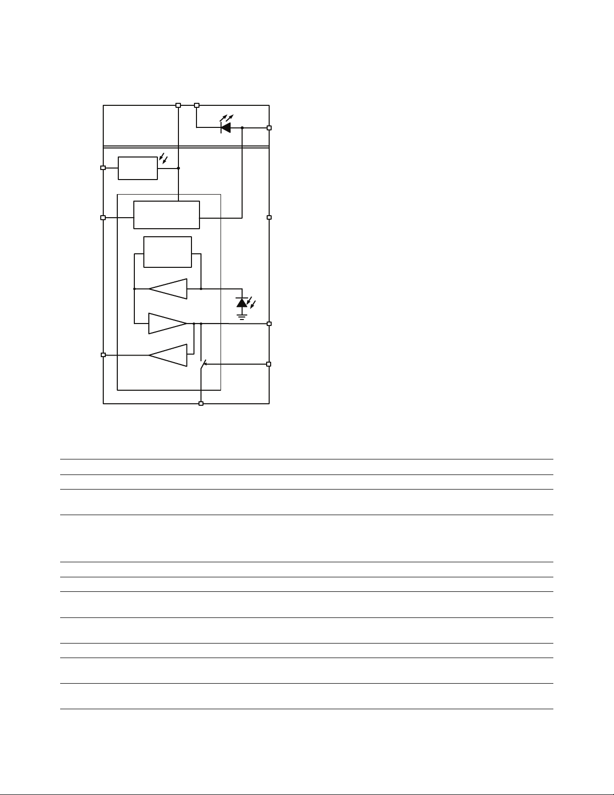
Functional Block Diagram
(7) ALS_IOUT
(2) LEDON
(3) PS_DOUT
Ambient Light
Sensor
LED Driver with
Stuck High Protection
Cancellation
V-I Converter
Hysteresis
Comparator
Proximity Sensor ASIC
(4) Vcc
Sunlight
TIA
(10) LEDK
(1) NC
LED
(5) NC
PIN
(6) PS_PFILT
(9) PS_ENB
(8) GND
I/O Pins Configuration Table
Pin Symbol Type Description
1 NC – No Connection
2 LEDON Digital I/P LED Driver Input
LEDA will turn off when LEDON is stuck in high state for > Max-PW
3 PS_DOUT Digital O/P PS Digital Output
(Open drain output that requires a pull-up resistor of recommended value 10kΩ)
PS_DOUT = LOW when PS_VPFILT > VTH
PS_DOUT = HIGH when PS_VPFILT < VTH
4 Vcc Supply Voltage Supply
5 NC – No Connection
6 PS_PFILT Analog O/P PS Analog Output
Connect to integration circuit (R3 and C3)
7 ALS_IOUT Analog O/P ALS analog current output
Connect to external load resistor R4. Recommended value 1kΩ.
8 GND Ground Ground
9 PS_ENB Digital I/P PS Power Down Enable
ENB = 0 Normal mode operation, ENB = 1 Shut down mode
10 LEDK Analog O/P Connect to Cathode of LED (proximity sensor)
External current limiting resistor is used to control current flow in the LED
2

Ordering Information
Part Number Packaging Quantity
APDS-9800-021 Tape & Reel 2500 per reel
Absolute Maximum Ratings
Parameter Symbol Min. Max. Units Conditions
Supply Voltage V
Input Logic Voltage VI 0 4 V TA = 25°C
Reflow Soldering Temperature 260 °C
CC
0 4 V TA = 25°C
Recommended Operating Conditions
Parameter Symbol Min. Max. Units Conditions
Operating Temperature T
Storage Temperature T
Supply Voltage V
A
S
CC
-40 85 °C
-40 85 °C
2.4 3.6 V
3

Electrical & Optical Specifications (Ta=25°C)
Parameters Symbol Minimum Typical Maximum Units Conditions
ALS+PS Module
Shutdown Current I
SD
Idle Current Icc 325 500 675 μA Vcc = 3 V, PS_ENB = 0 V, Lux = 0
ALS Output
Photo Current I_PH1 15 26 – μA Vcc =3 V, Lux = 100
Dark Current I_DARK – 300 – nA Vcc = 3 V, Lux = 0
Light Current Ratio – 1.2 – – Incandescent / Fluorescent
Rise Time Tr – 5 – ms R4 = 1k Ω, Lux = 100
Fall Time Tf – 5 – ms R4 = 1k Ω, Lux = 100
Propagation delay Td – 5 – ms R4 = 1k Ω, Lux = 100
Saturation voltage Vsat 1.0 – – V R4 = 150k Ω, Vcc = 3 V, Lux = 100
PS Input
Logic High Voltage, LEDON V
Logic High Voltage, PS_ENB V
Logic Low Voltage, LEDON V
Logic Low Voltage, PS_ENB V
Logic High Input Current, LEDON I
Logic High Input Current, PS_ENB I
Logic Low Input Current, LEDON I
Logic Low Input Current, PS_ENB I
IH
IH
IL
IL
IH
IH
IL
IL
PS Output
Analog Output VPFILT 0.65 1.9 3.0 V VCC = 3 V, ENB = 0 V,
Digital Output Low Level, PS_DOUT V
OL
Crosstalk VPFILT
@
Crosstalk
Max I
I
Pulse Width Max-PW – 120 – μs Vcc = 3 V, PS_ENB = 0 V
LED
Pulse Current I
LED
LED
Transmitter
Rise Time (LEDA) T
Fall Time (LEDA) T
R
F
PS Receiver
Rise Time(PS_DOUT) T
Fall Time(PS_DOUT) T
R
F
PS Hysteresis Comparator
Hysteresis V
Threshold Voltage V
HYS
TH
PS Sunlight Cancellation
Sun Light Illuminance Isun 100K Lux Vcc= 3 V
Note:
1. White LED is used as light source.
– 0.3 1 μA Vcc = 3 V, PS_ENB = 3 V, Lux = 0
(1)
1.8 – – V
1.8 – – V
0 – 0.3 V
0 – 0.3 V
– 0.1 1 μA VI ≥ V
– 0.1 1 μA VI ≥ V
– 0.1 1 μA VI ≤ V
– 0.1 1 μA VI ≤ V
0 – 0.4 V
IH
IH
IL
IL
LEDON = 10k Hz, 50% DC,
50 pulses; R3 = 1M ohm,
C3 = 3.3 nF;
Kodak 18% Grey card at
detectable distance = 20 mm
from the APDS-9800.
0 – 0.2 V VCC = 3 V, ENB = 0 V,
LEDON = 10k Hz, 50% DC,
50 pulses; R3 = 1M ohm,
C3 = 3.3 nF;
No blocking object
– 120 – mA Vcc = 3 V, R1 = 10 Ω
– 40 – ns Vcc = 3 V , ILED = 120 mA,
– 40 – ns
Freq = 10k Hz
– 1 – μs Vcc = 3 V, R2 = 10k Ω,
– 1 – μs
Frequency = 10k Hz
– 40 – mV Vcc= 3 V
– 655 – mV Vcc= 3 V
4

Typical Application Circuit
R1
PWM/GPIO
MCU
ADC
GPIO
GPIO
ADC
C1 C2
(7) ALS_IOUT
R4
(2) LEDON
Vdd
R2
(3) PS_DOUT
(4) Vcc
Ambient
Light
C4
Sensor
LED Driver with
Stuck High
Protection
Sunlight
Cancellation
V-I Converter
Hysteresis
Comparator
Proximity Sensor ASIC
(10) LEDK
(1) NC
LED
(5) NC
TIA
PIN
(6) PS_PFILT
R3C3
(9) PS_ENB
(8) GND
Component Recommended Values
R1 10 Ω
R2 10k Ω
R3 1M Ω
R4 1k Ω
C1 100 nF
C2 6.8 uF
C3 3.3 nF
C4 10 uF
Note: Do NOT make connects to the NC pins.
5

Ambient Light Sensor Performance Chart
1
0.9
0.8
0.7
0.6
0.5
0.4
RESPONSE (a.u.)
0.3
0.2
0.1
0
300 400 500 600 700 800 900 1000 1100
WAVELENGTH (nm)
Figure 1. Normalized Sensor Spectral Response Figure 2. ALS Average Iout versus Lux (Vcc = 3.0V, T=25°C, White LED source)
1000
900
800
700
600
500
IDARK (nA)
400
300
200
100
0
-40 -20 0 20 40 60 80 100
TEMPERATURE (°C)
APDS-9800
Eye Response
300
250
200
150
IOUT (µA)
100
50
0
0 100 200 300 400 500 600 700 800 900 1000 1100 1200
LIGHT INTENSITY (LUX)
Vcc
ENB
LEDON
PFILT
DOUT
>50ns
>20us
V
TH
Burst Pulses
Figure 3. ALS Dark Current versus Temperature (Vcc = 3.0V) Figure 4. Proximity Sensor Typical Timing Waveforms
Proximity Sensor Performance Charts
0.7
0.6
0.5
0.4
0.3
TYPICAL ILED (A)
0.2
0.1
0
2 3 4 5 6 7 8 9 10
RLED (OHM)
Figure 5. ILED versus RLED (TA=25°C) Figure 6. Normalized Idle Icc versus Temperature (Vcc =3V)
6
Vcc=2.4V
Vcc=2.7V
Vcc=3V
Vcc=3.3V
Vcc=3.6V
1.20
1.10
1.00
0.90
NORMALIZED ICC-IDLE
0.80
0.70
-60 -40 -20 0 20 40 60 80 100
TEMPERATURE (°C)

APDS-9800 Package Outline
A A
1.230.98
LED
0.15
TOP VIEW
ALS
4.95
+ 0.20
0
0.43
0.56
0.56
0.73
1.19
1.80
0.38 0.70 0.70 0.70 0.38
2.20
1 2 3 4 5
0.38
0.38
0.07
0.38
SIDE VIEW
Photo Detector
1.45±0.10
0.711.19
0
+ 0.2
3
0.40
678910
0.15
0.40
0.38
Notes:
1. All dimensions are in millimeters.
2. Standard tolerance, unless otherwise stated:
PIN CONFIGURATION
Pin 1: NC
Pin 2: LEDON
Dimension
Pin 3: PS_DOUT
Decimal
Pin 4: VCC
Pin 5: NC
XX ±0.5 mm
Pin 6: PS_PFILT
XX.X ±0.2 mm
Pin 7: ALS_IOUT
XX.XX ±0.1 mm
Pin 8: GND
Pin 9: PS_ENB
All others ±0.1 mm
Standard
Tolerance
Pin 10: LEDK
APDS-9800 Pin Configuration
1 2 3 4 5
7
BOTTOM VIEW
Recommended Land Pattern
0.50
Pin 1 : NC
0.90 0.90 0.90
Pin 2 : LEDON
Pin 3 : PS_DOUT
Pin 4 : VCCPin 5: NC
Pin 6 : PS_PFILT
Pin 7 : ALS_IOUT
2.30
Pin 8 : GND
Pin 9 : PS_ENB
Pin 10 : LEDKTOP
678910
0.18
Notes:
1. All dimensions are in millimeters.
2. Do NOT connect NC pins.
0.18
0.18
0.50
0.45
0.18
0.45

APDS-9800 Tape & Reel Dimensions
Tape Dimensions
8.00
+0.30
-0.10
4.00 ± 0.10
5.19 ± 0.10
8.00 ± 0.10
User Direction of Feed
8° MAX
1.68 ± 0.10
2.00 ± 0.05
Ø 1.50 ± 0.10
Ø 1.00 ± 0.05
0.25 ± 0.02
3.23 ± 0.10
A. K. B.
1.75 ± 0.10
3.50 ± 0.05
6° MAX
Reel Dimensions:
Unit: millimeter
W 330.0 ± 1.5
N 100.0 ± 1.5
T1 8.5 ± 0.2/-0.1
E 2.0 ± 0.5
T2 13.5 ± 0.2
C 13.0 ± 0.5/-0.2
8
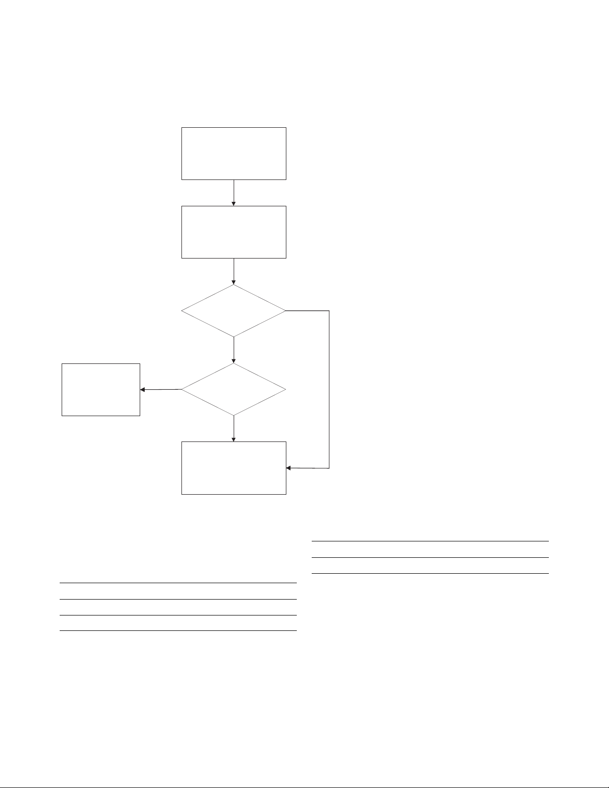
Moisture Proof Packaging
All APDS-9800 options are shipped in a moisture proof package. Once opened, moisture absorption begins. This part is
compliant to JEDEC Level 3.
Units in a sealed
moisture-proof
package
Package Is
opened (Unsealed)
Environment
less than 30 °C and less
than 60% RH ?
Yes
Baking
is not necessary
Yes
Package Is
open less
than 168 hours ?
No
Perform recommended
bake
Baking Conditions:
If the parts are not stored in dry conditions, they must be
baked before reflow soldering to prevent damage to the
parts.
Package Temperature Time
In Reel 60°C 48 hours
In Bulk 100°C 4 hours
Baking should only be done once.
No
Recommended Storage Conditions:
Storage Temperature 10°C to 30°C
Relative Humidity below 60% RH
Recommended Time from Unsealing to Soldering:
After removal from the bag, the parts should be soldered
within 168 hours if stored at the recommended storage
conditions. If times longer than 168 hours are needed, the
parts must be stored in a dry box.
9
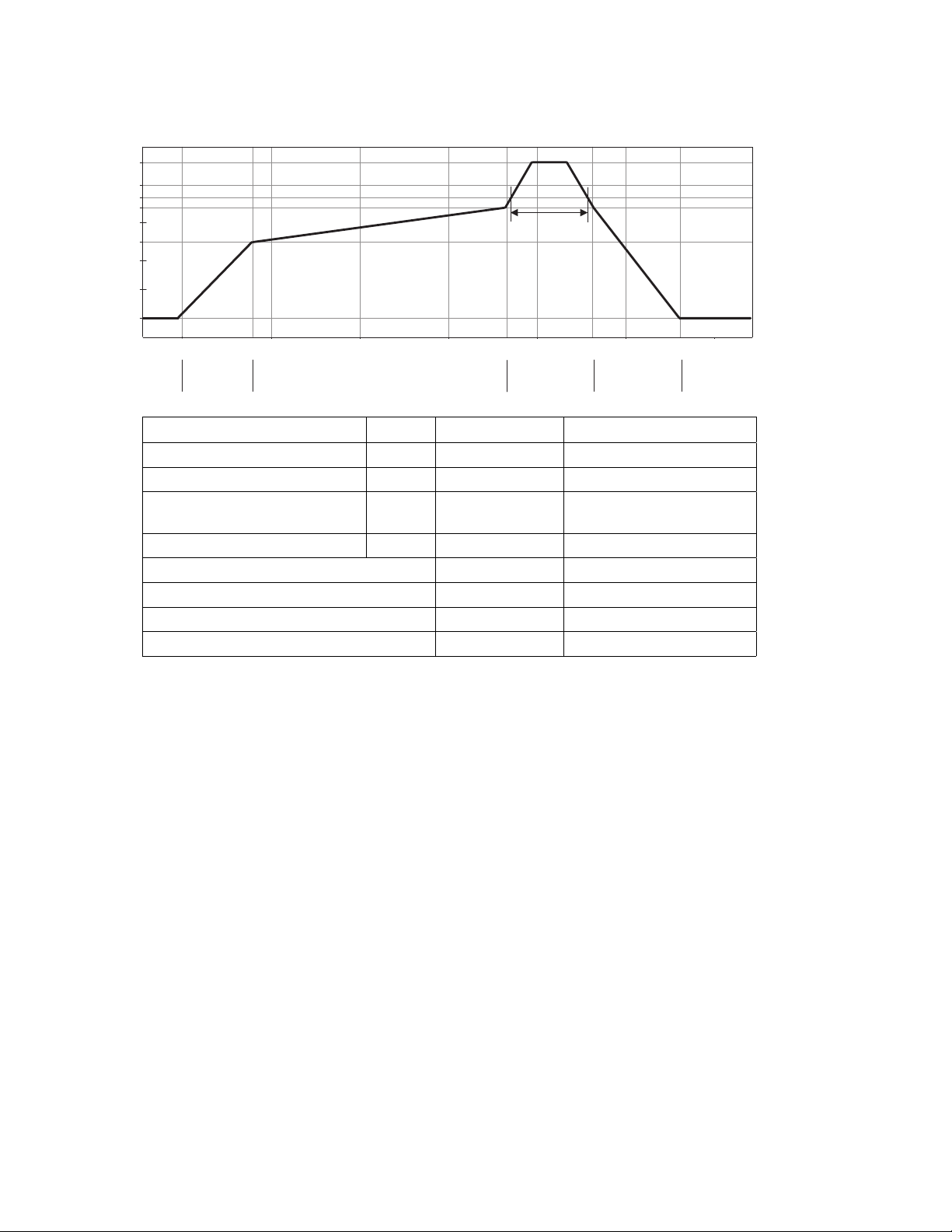
Recommended Reflow Profile
255
230
217
200
180
150
120
T - TEMPERATURE (°C)
80
25
0
R1
P1
HEAT
UP
R2
50 100 300150 200 250
P2
SOLDER PASTE DRY
MAX 260C
R3
60 sec to 90 sec
Above 217 C
P3
SOLDER
REFLOW
R4
R5
P4
COOL DOWN
Process Zone Symbol ∆T Maximum ∆T/∆time or Duration
Heat Up P1, R1 25°C to 150°C 3°C/s
Solder Paste Dry P2, R2 150°C to 200°C 100s to 180s
Solder Reflow P3, R3
P3, R4
Cool Down P4, R5 200°C to 25°C -6°C/s
Time Maintained Above Liquidus Point, 217°C > 217°C 60s to 120s
Peak Temperature 260°C –
Time within 5°C of Actual Peak Temperature > 255°C 20s to 40s
Time 25°C to Peak Temperature 25°C to 260°C 8minutes
200°C to 260°C
260°C to 200°C
3°C/s
-6°C/s
t-TIME
(SECONDS)
The reflow profile is a straight-line representation of
a nominal temperature profile for a convective reflow
solder process. The temperature profile is divided into
four process zones, each with different ∆T/∆time temperature change rates or duration. The ∆T/∆time rates or
duration are detailed in the above table. The temperatures
are measured at the component to printed circuit board
connections.
In process zone P1, the PC board and component pins are
heated to a temperature of 150°C to activate the flux in
the solder paste. The temperature ramp up rate, R1, is
limited to 3°C per second to allow for even heating of both
the PC board and component pins.
Process zone P2 should be of sufficient time duration (100
to 180 seconds) to dry the solder paste. The temperature
is raised to a level just below the liquidus point of the
solder.
Process zone P3 is the solder reflow zone. In zone P3, the
temperature is quickly raised above the liquidus point of
solder to 260°C (500°F) for optimum results. The dwell time
above the liquidus point of solder should be between 60
and 120 seconds. This is to assure proper coalescing of the
solder paste into liquid solder and the formation of good
solder connections. Beyond the recommended dwell
time the intermetallic mm growth within the solder connections becomes excessive, resulting in the formation of
weak and unreliable connections. The temperature is then
rapidly reduced to a point below the solidus temperature
of the solder to allow the solder within the connections to
freeze solid.
Process zone P4 is the cool down after solder freeze. The cool
down rate, R5, from the liquidus point of the solder to
25°C (77°F) should not exceed 6°C per second maximum.
This limitation is necessary to allow the PC board and
component pins to change dimensions evenly, putting
minimal stresses on the component.
It is recommended to perform reflow soldering no more
than twice.
10

Window and Light Guide Recommendations
Transparent window with IR coating (IR pass of around 90% and minimum 30% visible pass) is recommended in order to
pass both visible and infrared light. The material of the window is recommended to be polycarbonate. The surface finish
of the plastic should be smooth, without any texture.
The recommended plastic material for use as a window is available from Bayer AG and Bayer Antwerp N. V. (Europe),
Bayer Corp.(USA) and Bayer Polymers Co., Ltd. (Thailand), as shown in Table below.
Recommended Plastic Materials
Material number Visible light transmission* Refractive index
Makrolon LQ2647 87% 1.587
Makrolon LQ3147 87% 1.587
Makrolon LQ3187 85% 1.587
* Transmittance of visible light will reduce if plastic window is coated with IR ink
To ensure that the performance of the APDS-9800 will not be affected by improper window design, there are some
constraints on the dimensions and design of the window so that the maximum size of the window, which is placed in
front of the photo light sensor, will not affect the angular response of the APDS-9800. This maximum dimension that is
recommended will ensure an acceptable light reception cone.
Plastic Window
IR absorbing area
IR pass area
0.7 mm
Air gap
APDS-9800
Side view of IR pass areas for window design
1.2 mm
3 mm
0.7 mm
Top view of IR pass areas for window design
Windows thickness
Filter
IR pass areas
The distance between the bottom of the window and the sensor top–the air gap– should be as close as possible and not
more than 0.2 mm. For optimum performance, windows thickness should be limited to not more than 0.8mm.
For product information and a complete list of distributors, please go to our web site: www.avagotech.com
Avago, Avago Technologies, and the A logo are trademarks of Avago Technologies in the United States and other countries.
Data subject to change. Copyright © 2005-2009 Avago Technologies. All rights reserved.
AV02-2132EN - September 7, 2009
 Loading...