

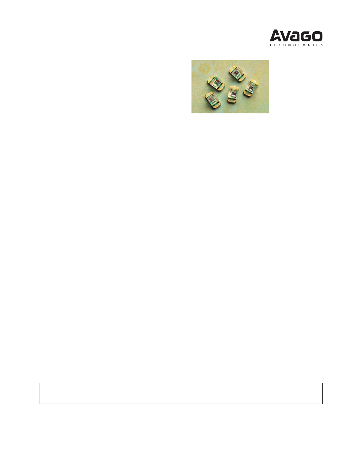
APDS-9004
Miniature Surface-Mount Ambient Light Photo Sensor
Data Sheet
Description
The APDS-9004 is a low cost analog-output ambient
light photo sensor in miniature chipLED lead-free,
reverse surface mount package. It consists of a photo
sensor, whose spectral response is close to CIE standard
photopic observer. Hence, it provides an excellent
responsivity that is close to the response of human
eyes, as shown in Figure 2. It is suitable for portable
applications with its ultra small package design.
The APDS-9004 is ideal for applications in which the
measurement of ambient light is used to control
display backlighting. Mobile appliances such as the
mobile phones and PDAs that draw heavy current from
display backlighting will benefit from incorporating
these photo sensor products in their designs by
reducing power consumption significantly.
Features
• Spectral responsivity close to that of human eye
• ChipLED Reverse surface-mount package
Height – 1.10mm
Width – 3.20mm
Depth – 1.60mm
• Good output linearity across wide illumination
range
• Low sensitivity variation across various light
sources
• Operating temperature
-40°C to 85°C
• Vcc supply 2.4 to 5.5V
• Lead-free package, RoHS compliance.
Applications
• Detection of ambient light to control display
backlighting
- Mobile devices – Mobile phones, PDAs
- Computing devices – Notebooks, Webpads
- Consumer devices – TVs, Video Cameras, Digital
Still Cameras
• Automatic Residential and Commercial Lighting
Management
• Electronic Signs and Signals
CAUTION: It is advised that normal static precautions be taken in handling and assembly
of this component to prevent damage and/or degradation which may be induced by ESD.
Application Support Information
The Application Engineering Group is available to assist
you with the application design associated with APDS9004 ambient light photo sensor module. You can
contact them through your local sales representatives
for additional details.
Ordering Information
Part Number Packaging Type Package Quantity
APDS-9004-020 Tape and Reel 4-pins Chipled package 2500
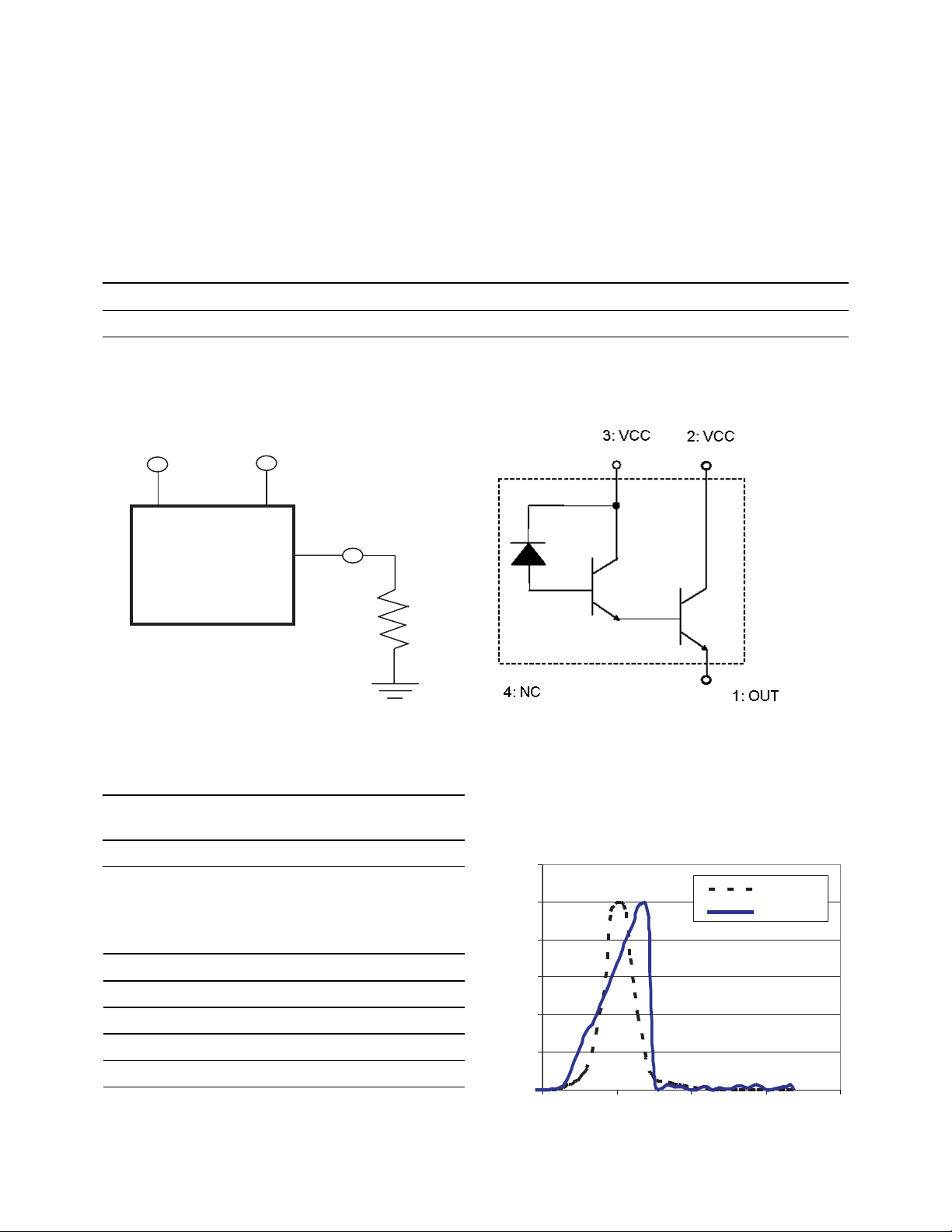
Typical Application Circuit APDS-9004 Block Diagram
Pin 3:V
CC
APDS -9004
Pin 2:V
CC
Pin 1:OUT
Pin 4:NC
Figure 1. Typical application circuit for APDS-9004
Figure 1 Table
Component Recommended Application
Circuit Component
R
LOAD
1k ohm
I/O Pins Configuration Table
R
LOAD
Notes : PIN 2 and PIN 3 Vcc need to be externally shorted.
Figure 2. Relative Spectral Response Vs. Wavelength
Relative Spectral Response Vs. Wavelength
Relative Spectral Response Vs Wavelength
1.2
Eye
1
0.8
APDS-9004
Pin Symbol Description
1 OUT OUT
2VCC VCC
3VCC VCC
4NC No Connect
2
0.6
0.4
Relative Spectral Response
0.2
0
350 550 750 950 1150
Wavelength (nm)

Absolute Maximum Ratings
For implementations where case to ambient thermal resistance is ≤ 50 °C /W
Parameter Symbol Min. Max. Units
Storage Temperature T
Operating Temperature T
Supply Voltage V
S
A
CC
-40 85 °C
-40 85 °C
06.0V
Recommended Operating Conditions
Parameter Symbol Min. Max. Units
Supply Voltage V
CC
2.4 5.5 V
Electrical & Optical Specifications (Ta=25
°°
°C)
°°
Parameter Symbol Min. Typ. Max. Units Conditions
Output Current (I)[note4] I
_OUT1
3 19 31 uA Vcc=3.0V, Lux=10
[Note 2]
Output Current (II)[note4] I
_OUT2
90 230 370 uA Vcc=3.0V, Lux=100
[Note 2]
Output Current (III)[note4] I
_OUT3
- 276 - uA Vcc=3.0V, Lux=100
[Note 1]
Dark Current I
Light Current Ratio I
Saturation Output Voltage V
_DARK
_OUT3
O
/ I
_OUT2
- - 0.5 uA Vcc=5.0V,Lux=0
-1.2--
2.2 2.32 - V Vcc=3.0V, Lux=100,
Rload=1M
Peak Sensitivity Wavelength - 620 - nm
Settling Time with pulsed Vcc Tset 3.5 ms Vcc pulse = 0V to 3V,
Rload=1kΩ, Lux=100
[Note 3]
Propagation Delay time Td - 600 - us Vcc=3.0V, Lux=100,
Rload=1k Ω [Note 3]
Storage Delay time Ts - 200 - us Vcc=3.0V, Lux=100,
Rload=1k Ω [Note 3]
Rise Time Tr - 0.95 ms Vcc=3.0V, Lux=100,
Rload=1kΩ [Note 3]
Fall Time Tf - 0.8 ms Vcc=3.0V, Lux=100,
Rload=1kΩ[Note 3]
Note:
1. Illuminance by Incandescent lamp
2. Fluorescent light is used as light source. White LED is substituted in mass production.
3. White LED is used as light source.
4. Other binning options are available. Please contact your Avago Technologies representative for information on current available bins
3
Relative Iout
Relative Iout
APDS-9004 Performance Charts
10000
1000
100
Average Iout(uA)
10
1
1.10
1.08
1.06
1.04
1.02
1.00
Relative output current
0.98
0.96
Average Iout Vs Lux (Vcc=3V,T=25C)
White LED
10 100 1000
Lux
Relative Output current Vs Vcc ( T=25C, 100 Lux)
2 2.5 3 3.5 4 4.5 5 5.5 6
Vcc(V)
Relative Output Current Vs Temperature (Vcc=3V, 100 Lux)
2.50
2.00
1.50
1.00
Relative Iout(A)
0.50
0.00
-50 -25 0 25 50 75 100
1.20
1.00
0.80
0.60
Relative Iout
0.40
0.20
0.00
-90 -60 -30 0 30 60 90
Temp(C)
Relative Iout Vs Angle
Relative output current
Angle
4
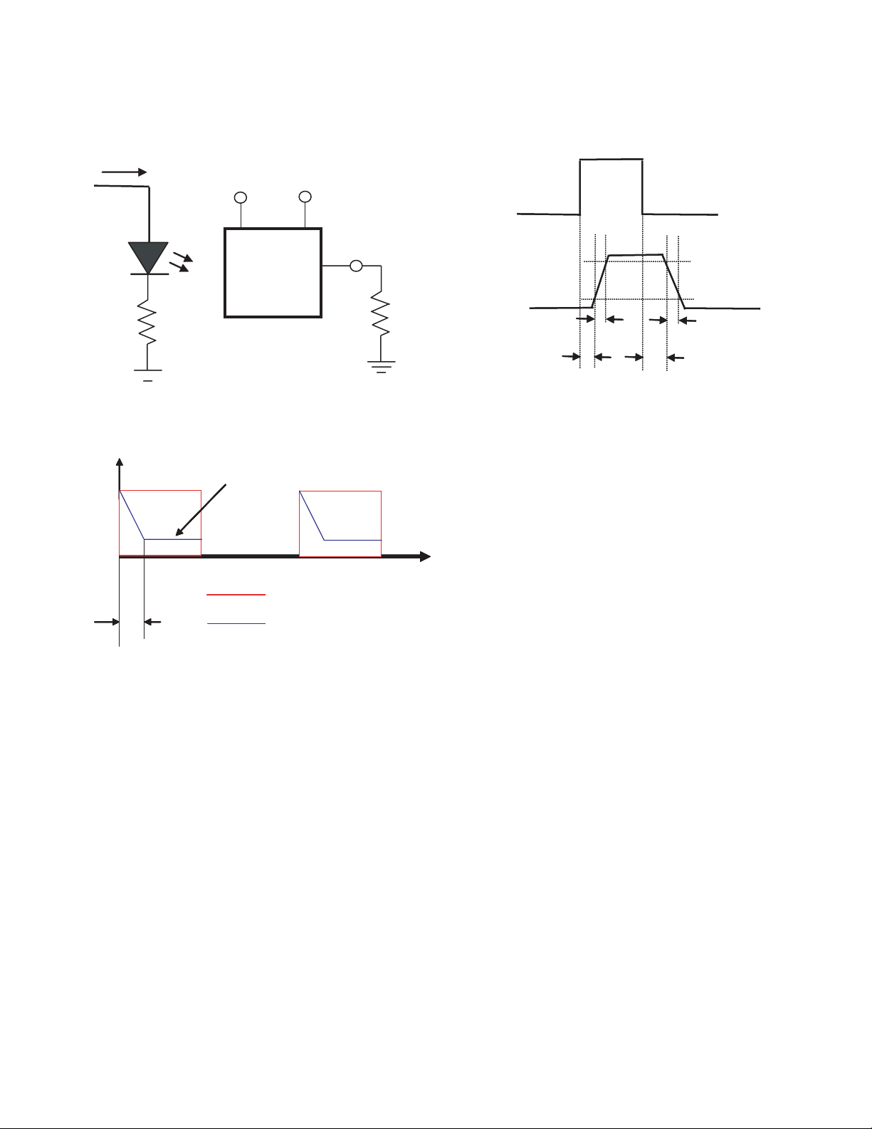
APDS-9004 Light Measurement Circuit and Waveforms
I_pulse
Pin 3:V
CC
Pin 2:V
CC
Pin 1:OUT
APDS-9004
Pin 4:NC
sensor-output attains ~95% of
its voltage magnitude
corresponds to the set light level
R
LOAD
I_pulse
I_pulse
GND
GND
VOUT
VOUT
td
td
90%
90%
10%
10%
tr
tr
tf
tf
ts
ts
Tset
VCC Pulse from PG
Sensor Output at load
5

APDS-9004 Package Outline
6

APDS-9004 Tape and Reel Dimensions
7

Moisture Proof Packaging Chart
All APDS-9004 options are shipped in moisture proof
package. Once opened, moisture absorption begins.
This part is compliant to JEDEC Level 3.
Baking conditions
If the parts are not stored in dry conditions, they must
be baked before reflow to prevent damage to the parts.
Package Temp. Time
In Reels 60°C 48 hours
In Bulk 100°C 6 hours
Baking should only be done once.
8
Recommended Storage Conditions
Storage Temperature 10°C to 30°C
Relative Humidity Below 60% RH
Time from Unsealing to Soldering
After removal from the bag, the parts should be
soldered within seven days if stored at the
recommended storage conditions. If times longer than
seven days are needed, the parts must be stored in a
dry box.

Recommended Reflow Profile
255
230
217
200
180
150
120
80
T - TEMPERATURE (°C)
25
R1
0
P1
HEAT
UP
R2
50
100 150 200 250 300
P2
SOLDER PASTE DRY
MAX 260°C
R3
60 sec to 90 sec
Above 217 °C
P3
SOLDER
REFLOW
R4
R5
P4
COOL DOWN
t-TIME
(SECONDS)
Process Zone Symbol T Maximum ∆T/ time or Duration
Heat Up P1, R1 25°C to 150°C 3°C/s
Solder Paste Dry P2, R2 150°C to 200°C 100s to 180s
Solder Reflow P3, R3
P3, R4
200°C to 255°C
255°C to 200°C
3°C/s
-6°C/s
Cool Down P4, R5 200°C to 25°C -6°C/s
Time maintained above 217°C > 217°C 60s to 90s
Peak Temperature 260°C
Time within 5°C of actual Peak Temperature > 255°C 20s to 40s
Time 25°C to Peak Temperature 25°C to 260°C 8mins
The reflow profile is a straight-line representation of a
nominal temperature profile for a convective reflow
solder process. The temperature profile is divided into
four process zones, each with different ∆T/∆time
temperature change rates or duration. The ∆T/∆time
rates or duration are detailed in the above table. The
temperatures are measured at the component to
printed circuit board connections.
In process zone P1, the PC board and APDS-9004 pins
are heated to a temperature of 150°C to activate the
flux in the solder paste. The temperature ramp up rate,
R1, is limited to 3°C per second to allow for even
heating of both the PC board and APDS-9004 pins.
Process zone P2 should be of sufficient time duration
(100 to 180 seconds) to dry the solder paste. The
temperature is raised to a level just below the liquidus
point of the solder, usually 200°C (392°F).
Process zone P3 is the solder reflow zone. In zone P3,
the temperature is quickly raised above the liquidus
point of solder to 255°C (491°F) for optimum results.
The dwell time above the liquidus point of solder
should be between 20 and 40 seconds. It usually takes
about 20 seconds to assure proper coalescing of the
solder balls into liquid solder and the formation of good
solder connections. Beyond a dwell time of 40 seconds,
the intermetallic growth within the solder connections
becomes excessive, resulting in the formation of weak
and unreliable connections. The temperature is then
rapidly reduced to a point below the solidus
temperature of the solder, usually 200°C (392°F), to
allow the solder within the connections to freeze solid.
Process zone P4 is the cool down after solder freeze.
The cool down rate, R5, from the liquidus point of the
solder to 25°C (77°F) should not exceed 6°C per second
maximum. This limitation is necessary to allow the PC
board and APDS-9004 pins to change dimensions
evenly, putting minimal stresses on the APDS-9004.
It is recommended to perform reflow soldering no
more than twice.
9

Appendix A: SMT Assembly Application Note
Solder Pad, Mask and Metal
Stencil
Aperture
Solder
Mask
Figure 1. Stencil and PCBA
1.1 Recommended Land Pattern
Metal Stencil
For Solder
Paste
Printing
Land
Pattern
PCBA
Slot Opening for APDS9004 to be exposed on the
Reverse Side of the PCBA
Soldering
C
L
Terminal
1.00
0.945
Slot Opening for
APDS-9004 to be
exposed on the
Reverse Side of
the PCBA
0.60
Figure 2. Recommended Land Pattern
0.50
2.00
0.71
1.89
0.71
0.60
Unit: mm
Tolerance: +/- 0.2
10

1.2 Recommended Metal Solder Stencil Aperture
It is recommended that a 0.11 mm (0.004 inches) thick
stencil be used for solder paste printing. Aperture
opening for shield pad is 0.6mm x 0.71mm. This is to
ensure adequate printed solder paste volume and no
shorting.
Aperture
Opening
0.11
3.31
Figure 3. Solder stencil aperture
1.3 Adjacent Land Keepout and Solder Mask Areas
Adjacent land keep-out is the maximum space
occupied by the unit relative to the land pattern. There
should be no other SMD components within this area.
The minimum solder resist strip width required to avoid
solder bridging adjacent pads is 0.2 mm.
Note: Wet/Liquid Photo-Imageable solder resist/mask
is recommended.
2.7
1.7
Unit: mm
Mounting
Center
Unit:
mm
0.2
MIN.
Figure 4. Adjacent land keepout and solder mask areas.
11
4.31
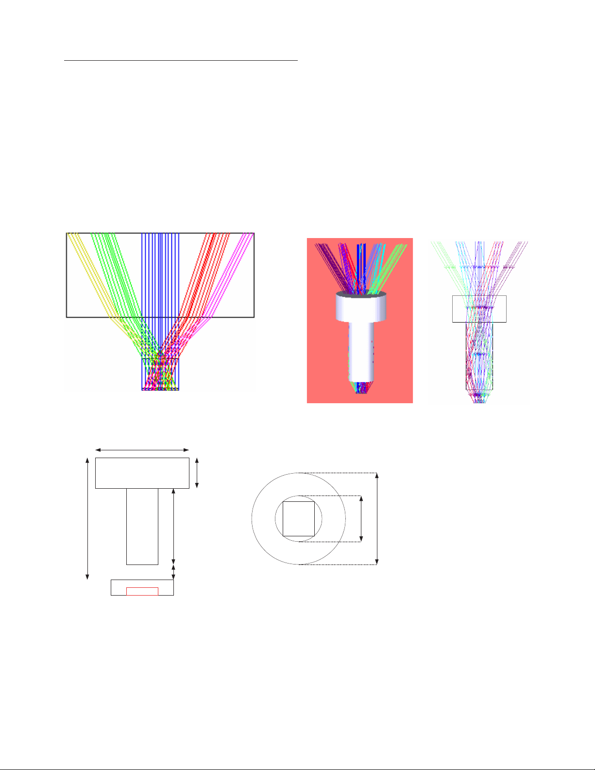
Appendix B: Optical Window Design for APDS-9004
Optical Window Dimensions
To ensure that the performance of the APDS-9004 will
not be affected by improper window design, there are
some constraints on the dimensions and design of the
window. There is a constraint on the minimum size of
the window, which is placed in front of the photo light
sensor, so that it will not affect the angular response
of the APDS-9004. This minimum dimension that is
recommended will ensure at least a ±35° light
reception cone.
If a smaller window is required, a light pipe or light
guide can be used. A light pipe or light guide is a
Flat
APDS-9004
cylindrical piece of transparent plastic, which makes
use of total internal reflection to focus the light.
The thickness of the window should be kept as
minimum as possible because there is a loss of power
in every optical window of about 8% due to reflection
(4% on each side) and an additional loss of energy in
the plastic material.
Figure 5a and 5b illustrate the two types of window
that we have recommended which could either be a
flat window or a flat window with light pipe.
Figure 5(a). Window Size Determination for Flat Window Figure 5(b). Window Design of Flat Window with Light Guide
D1
Top View
T
WD
Light Receving Area
Figure 6. Recommended Window Dimensions
L
Z
APDS-9004
D2 D1
12
Table 1 and Figure 6 below show the recommended
dimensions of the window. These dimension values
are based on a window thickness of 1.0mm with a
refractive index 1.585.
WD: Working Distance between window front panel & APDS-9004
D1: Window Diameter
T: Thickness
L: Length of Light Pipe
D2: Light Pipe Diameter
Z: Distance between window rear panel and APDS-9004
Table 1: Recommended dimension for optical window
WD (T+L+Z) Flat Window Flat Window with Light Guide
ZD1 D1 L
1.5 0.5 2.1 - -
2.0 1.0 2.8 - -
2.5 1.5 3.5 - -
3.0 2.0 4.2 2.5 1.5
( All dimensions are in mm )
Note : Active area center to coincide with window
center (flat or with light guide).
The window should be placed directly on top of the
photo sensor to achieve better performance and if a
flat window with a light pipe is used, dimension D2
should be 1.5mm to optimize the performance of
APDS-9004.
2.1 Optical Window Material
The material of the window is recommended to be
polycarbonate. The surface finish of the plastic should
be smooth, without any texture.
The recommended plastic material for use as a window
is available from Bayer AG and Bayer Antwerp N. V.
(Europe), Bayer Corp.(USA) and Bayer Polymers Co., Ltd.
(Thailand), as shown in Table 2.
Table 2: Recommended Plastic Materials
Material number Visible light transmission Refractive index
Makrolon LQ2647 87% 1.587
Makrolon LQ3147 87% 1.587
Makrolon LQ3187 85% 1.587
13

Appendix C: General Application Guide for APDS-9004
The APDS-9004 is a low cost analog-output ambient
light photo sensor whose spectral response closely
emulates the human eyes. APDS-9004 consists of a
phototransistor that enables the photo sensor to
produce a high gain photo current to a sufficient level
that can be converted to voltage with a standard value
of external resistor. APDS-9004 is then easily integrated
into systems that use ADC input which is available for
sampling of the external source, as shown in figure 7
below.
The amount of converted voltage, Vout, is mainly
dependant proportionally on the photo current which
generated by the brightness of the light shone on the
photo sensor and the load resistor used, RL. Increasing
the brightness of the light or/and the load resistor will
increase the output voltage.
Brightness is measured as “LUX” unit, which describes
how intense a light source that our eyes perceive. LUX
meter is the equipment for “LUX” measurement. Light
sources with the same LUX level appear at the same
brightness to the human eyes.
Vcc
2,3
Light Source
APDS-9004
4
NC
Figure 7. Configuration of APDS-9004 being used directly
1
C
Selection of the load resistor RL will determine the
amount of current-to-voltage conversion in the circuit.
Light source e.g. fluorescent light consists of ac noise
about 100Hz frequency. A capacitor of 10uF, which
acting as a low-pass filter, is recommended to add in
parallel with the load resistor to by-pass this ripples.
Vout
RL
A/D
micro-
controller
For product information and a complete list of distributors, please go to our web site: www.avagotech.com
Avago, Avago Technologies, and the A logo are trademarks of Avago Technologies, Limited in the United States and other countries.
Data subject to change. Copyright © 2006 Avago Technologies Pte. All rights reserved.
AV01-0184EN - September 14, 2006
 Loading...