


AFBR-57J7APZ
Digital Diagnostic SFP, 850nm 6.144/7.3728 Gb/s,
RoHS OBSAI/CPRI Compatible Optical Transceiver
Data Sheet
Description
Avago’s AFBR-57J7APZ optical transceiver supports
high speed serial links over multimode optical ber at
signaling rates up to 7.4 Gb/s for wireless base station applications involving the OBSAI or CPRI protocols, as well
as related applications. The transceiver is compliant with
Small Form Pluggable (SFP) multi-source agreements INF8074 and SFF-8472 for mechanical and electrical specications and FOCIS/IEC specications for optical duplex LC
connectors.
As an enhancement to the conventional SFP interfaced
dened in INF-8074, the AFBR-57J7APZ is compliant to
SFF-8472 (Digital Diagnostic Interface for Optical Transceivers). Using the 2-wire serial interface dened in SFF8472, the transceiver provides real time temperature,
supply voltage, laser bias current, laser average output
power and received input power. This information is in
addition to conventional SFP base data. The digital diagnostic interface also adds the ability to disable the transmitter and monitor the status of transmitter fault and
receiver loss of signal.
Related Products
• AFBR-57J5APZ: 850nm +3.3V LC SFP
for CPRI/OBSAI Applications
• AFCT-57J5APZ: 1310nm +3.3V LC SFP
for CPRI/OBSAI Applications
• AFCT-57J5ATPZ: 1310nm +3.3V LC SFP
for CPRI/OBSAI Applications
• AFBR-57D7APZ: 850nm +3.3V LC SFP
for 8.5/4.25/2.125 GBd Fibre Channel
• AFCT-57D5ATPZ: 1310nm +3.3V LC SFP
for 8.5/4.25/2.125 GBd Fibre Channel
• AFCT-57J7ATPZ: 1310nm +3.3V LC SFP
for CPRI/OBSAI Applications
Features
• Fully RoHS Compliant
• Diagnostic Features Per SFF-8472 “Diagnostic
Monitoring Interface for Optical Transceivers”
• Real time monitors of:
o Transmitted Optical Power
o Received Optical Power
o Laser Bias Current
o Temperature
o Supply Voltage
• Industrial Temperature and Supply Voltage Operation
(-40°C to 85°C) (3.3V ± 10%)
• Transceiver Specications per SFP (INF-8074) and SFF-
8472 (revision 10)
• Up to 200m with 50μm OM3 for 7.3728 Gb/s
• Up to 300m with 50μm OM3 for OBSAI 6.144 Gb/s
• LC Duplex optical connector interface conforming to
ANSI TIA/EIA604-10 (FOCIS 10A)
• 850nm Vertical Cavity Surface Emitting Laser (VCSEL)
Source Technology
• IEC 60825-1 Class 1/CDRH Class 1 laser eye safe
• Compatible with Fibre Channel and Gigabit Ethernet
applications
Applications
Wireless and cellular base station system interconnect
OBSAI rates 6.144 Gb/s, 3.072 Gb/s, 1.536 Gb/s
CPRI rates 7.3728 Gb/s, 4.9152 Gb/s, 2.4576 Gb/s,
1.2288 Gb/s
Digital Diagnostic Interface and Serial Identication
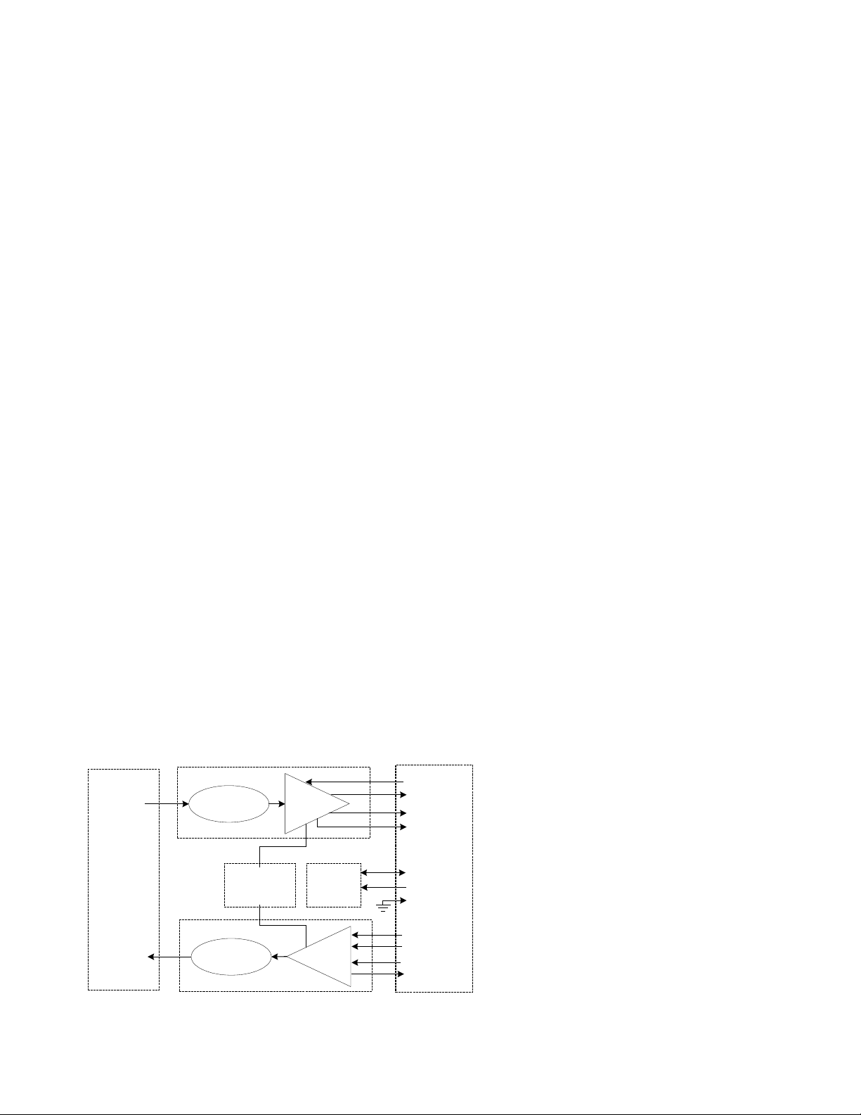
EEPROM
CONTROLLER
EEPROM
Photo-Detector
Amplification
&
Quantization
VCSEL
Laser Driver &
Safety Circuit
Electrical Interface
RD+ (Receive Data)
RD- (Receive Data)
Rx Loss Of Signal
MOD-DEF2 (SDA)
TX_DISABLE
TD+ (Transmit Data)
TD- (Transmit Data)
TX_FAULT
MOD-DEF0
MOD-DEF1 (SCL)
Receiver
Transmitter
Optical Interface
Light from Fiber
Light to Fiber
Rate Select
The 2-wire serial interface is based on ATMEL AT24C01A
series EEPROM protocol and signaling detail. Conventional EEPROM memory, bytes 0-255 at memory address
0xA0, is organized in compliance with INF-8074. New
digital diagnostic information, bytes 0-255 at memory
address 0xA2, is compliant to SFF-8472. The new diagnostic information provides the opportunity for Predictive Failure Identication, Compliance Prediction, Fault
Isolation and Component Monitoring.
Transmitter Section
The transmitter section includes consists of the Transmitter Optical SubAssembly (TOSA) and laser driver circuitry.
The TOSA, containing an 850nm VCSEL (Vertical Cavity
Surface Emitting Laser) light source, is located at the
optical interface and mates with the LC optical connector.
The TOSA is driven by a custom IC which uses the
incoming dierential high speed logic signal to modulate
the laser diode driver current. This Tx laser driver circuit
regulates the optical power at a constant level provided
the incoming data pattern is dc balanced (8B/10B code,
for example).
Transmit Disable (Tx_Disable)
The AFBR-57J7APZ accepts a TTL and CMOS compatible
transmit disable control signal input (pin 3) which shuts
down the transmitter optical output. A high signal implements this function while a low signal allows normal
transceiver operation. In the event of a fault (e.g. eye
safety circuit activated), cycling this control signal resets
the module as depicted in Figure 4. An internal pull up
resistor disables the transceiver transmitter until the host
pulls the input low. Host systems should allow a 10ms
interval between successive assertions of this control
signal. Tx_Disable can also be asserted via the twowire serial interface (address A2h, byte 110, bit 6) and
monitored (address A2h, byte 110, bit 7).
The contents of A2h, byte 110, bit 6 are logic OR’d with
hardware Tx_Disable (pin 3) to control transmitter
operation..
Transmit Fault (Tx_Fault)
A catastrophic laser fault will activate the transmitter
signal, TX_FAULT, and disable the laser. This signal is
an open collector output (pull-up required on the host
board). A low signal indicates normal laser operation
and a high signal indicates a fault. The TX_FAULT will
be latched high when a laser fault occurs and is cleared
by toggling the TX_DISABLE input or power cycling the
transceiver. The transmitter fault condition can also be
monitored via the two-wire serial interface (address A2,
byte 110, bit 2).
Eye Safety Circuit
The AFBR-57J7APZ provides Class 1 (single fault tolerant)
eye safety by design and has been tested for compliance
with the requirements listed in Table 1. The eye safety
circuit continuously monitors the optical output power
level and will disable the transmitter upon detecting an
unsafe condition beyond the scope of Class 1 certication. Such unsafe conditions can be due to inputs from
the host board (Vcc uctuation, unbalanced code) or a
fault within the transceiver.
Receiver Section
The receiver section includes the Receiver Optical SubAssembly (ROSA) and the amplication/quantization
circuitry. The ROSA, containing a PIN photodiode and
custom transimpedance amplier, is located at the
optical interface and mates with the LC optical connector.
The ROSA output is fed to a custom IC that provides postamplication and quantization.
Figure 1. Transceiver Functional Diagram
2

Receiver Loss of Signal (Rx_LOS)
The post-amplication IC also includes transition
detection circuitry which monitors the ac level of
incoming optical signals and provides a TTL/CMOS compatible status signal to the host (pin 8). An adequate
optical input results in a low Rx_LOS output while a high
Rx_LOS output indicates an unusable optical input. The
Rx_LOS thresholds are factory set so that a high output
indicates a denite optical fault has occurred. Rx_LOS
can also be monitored via the two-wire serial interface
(address A2h, byte 110, bit 1).
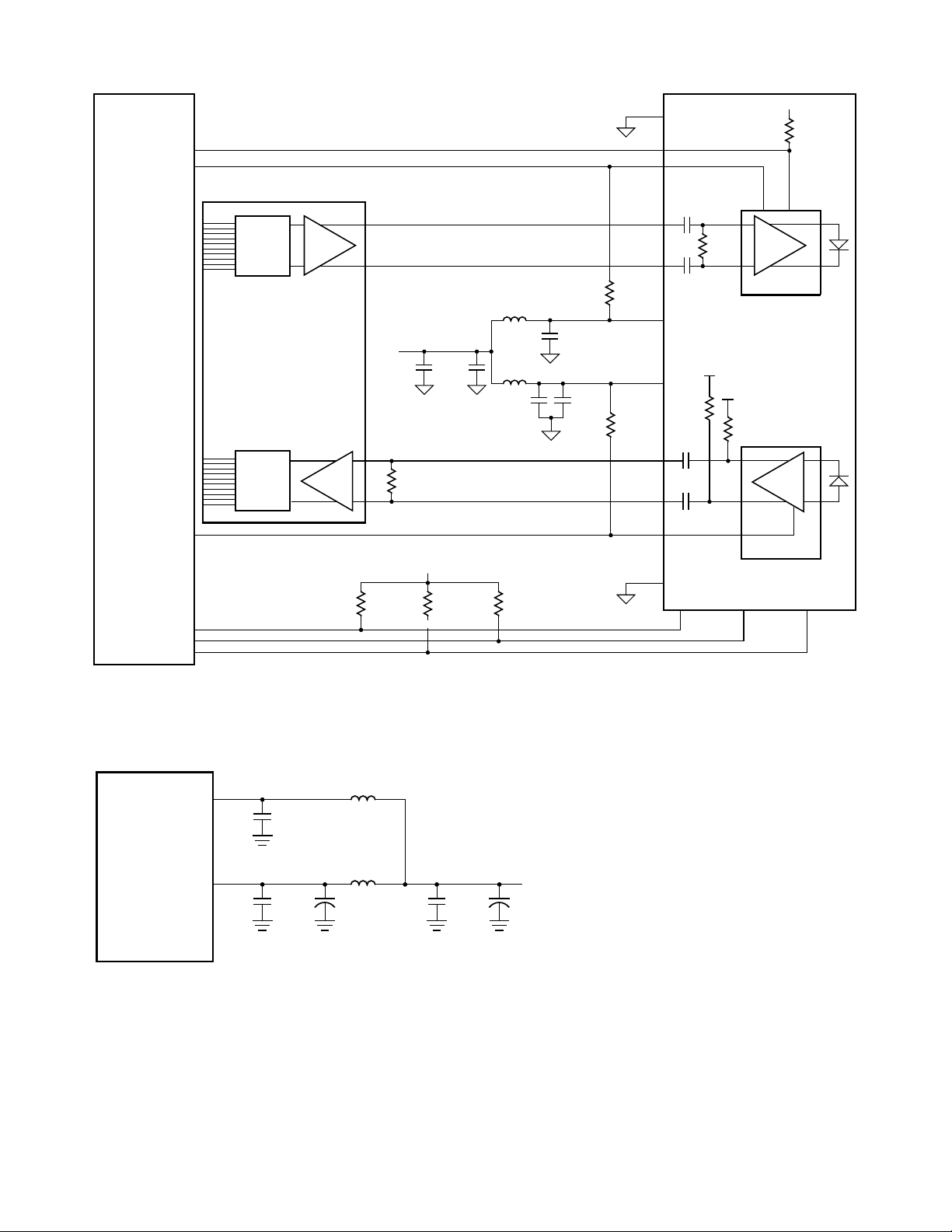
Functional Data I/O
The AFBR-57J7APZ interfaces with the host circuit board
through twenty I/O pins (SFP electrical connector) identied by function in Table 2. The board layout for this
interface is depicted in Figure 6.
The AFBR-57J7APZ high speed transmit and receive interfaces require SFP MSA, OBSAI or CPRI compliant signal
lines on the host board. To simplify board requirements,
biasing resistors and ac coupling capacitors are incorporated into the SFP transceiver module (per INF-8074) and
hence are not required on the host board. The Tx_Disable,
Tx_Fault, Rx_LOS and Rate_Select lines require TTL lines
on the host board (per INF-8074) if used. If an application
chooses not to take advantage of the functionality of
these pins care must be taken to ground Tx_Disable (for
normal operation) and Rate_Select is set to default in the
proper state.
Figure 2 depicts the recommended interface circuit to
link the AFBR-57J7APZ to supporting physical layer ICs.
Timing for MSA compliant control signals implemented
in the transceiver are listed in Figure 4.
Application Support
An Evaluation Kit and Reference Designs are available to
assist in evaluation of the AFBR-57J7APZ . Please contact
your local Field Sales representative for availability and
ordering details.
Caution
There are no user serviceable parts nor maintenance requirements for the AFBR-57J7APZ. All mechanical adjustments are made at the factory prior to shipment.
Tampering with, modifying, misusing or improperly
handling the AFBR-57J7APZ will void the product
warranty. It may also result in improper operation and
possibly overstress the laser source. Performance degradation or device failure may result. Connection of the
AFBR-57J7APZ to a light source not compliant with these
specications, operating above maximum operating
conditions or in a manner inconsistent with it’s design
and function may result in exposure to hazardous light
radiation and may constitute an act of modifying or man-
ufacturing a laser product. Persons performing such an
act are required by law to re-certify and re-identify the
laser product under the provisions of U.S. 21 CFR (Subchapter J) and TUV.
Ordering Information
Please contact your local eld sales engineer or one of
Avago Technologies franchised distributors for ordering
information. For technical information, please visit Avago
Technologies’ WEB page at www.Avago.com or contact
Avago Technologies Semiconductor Products Customer
Response Center at 1-800-235-0312. For information
related to SFF Committee documentation visit www.scommittee.org.
Regulatory Compliance
The AFBR-57J7APZ complies with all applicable laws
and regulations as detailed in Table 1. Certication level
is dependent on the overall conguration of the host
equipment. The transceiver performance is oered as a
gure of merit to assist the designer
Electrostatic Discharge (ESD)
The AFBR-57J7APZ is compatible with ESD levels found
in typical manufacturing and operating environments
as described in Table 1. In the normal handling and
operation of optical transceivers, ESD is of concern in two
circumstances.
The rst case is during handling of the transceiver prior
to insertion into an SFP compliant cage. To protect the
device, it’s important to use normal ESD handling precautions. These include using of grounded wrist straps, workbenches and oor wherever a transceiver is handled.
The second case to consider is static discharges to the
exterior of the host equipment chassis after installation.
If the optical interface is exposed to the exterior of host
equipment cabinet, the transceiver may be subject to
system level ESD requirements.
Electromagnetic Interference (EMI)
Equipment incorporating gigabit transceivers is typically
subject to regulation by the FCC in the United States,
CENELEC EN55022 (CISPR 22) in Europe and VCCI
in Japan. The AFBR-57J7APZ’s compliance to these
standards is detailed in Table 1. The metal housing and
shielded design of the AFBR-57J7APZ minimizes the EMI
challenge facing the equipment designer.
EMI Immunity (Susceptibility)
Due to its shielded design, the EMI immunity of the AFBR57J7APZ exceeds typical industry standards.
3

Flammability
BAUART
GEPRUFT
TYPE
APPROVED
TUV
Rheinland
Product Safety
¨
¨
The AFBR-57J7APZ optical transceiver is made of metal
and high strength, heat resistant, chemical resistant and
UL 94V-0 ame retardant plastic.
plant and remote transmitter. When operating out of requirements, the link cannot guarantee error free transmission.
Predictive Failure Identication
The AFBR-57J7APZ predictive failure feature allows a host
to identify potential link problems before system performance is impacted. Prior identication of link problems
enables a host to service an application via “fail over”
to a redundant link or replace a suspect device, maintaining system uptime in the process. For applications
where ultra-high system uptime is required, a digital SFP
provides a means to monitor two real-time laser metrics
associated with observing laser degradation and predicting failure: average laser bias current (Tx_Bias) and
Fault Isolation
The fault isolation feature allows a host to quickly
pinpoint the location of a link failure, minimizing
downtime. For optical links, the ability to identify a fault
at a local device, remote device or cable plant is crucial to
speeding service of an installation. AFBR-57J7APZ realtime monitors of Tx_Bias, Tx_Power, Vcc, Temperature and
Rx_Power can be used to assess local transceiver current
operating conditions. In addition, status ags Tx_Disable
and Rx Loss of Signal (LOS) are mirrored in memory and
available via the two-wire serial interface.
average laser optical power (Tx_Power).
Component Monitoring
Compliance Prediction:
Compliance prediction is the ability to determine if an
optical transceiver is operating within its operating and
environmental requirements. AFBR-57J7APZ devices
provide real-time access to transceiver internal supply
voltage and temperature, allowing a host to identify
potential component compliance issues. Received optical
power is also available to assess compliance of a cable
Table 1. Regulatory Compliance
Feature Test Method Performance
Electrostatic Discharge
(ESD) to the Electrical Pins
Electrostatic Discharge
(ESD) to the Duplex LC
Receptacle
Electrostatic Discharge
(ESD) to the Optical
Connector
Electromagnetic
Interference (EMI)
Immunity Variation of IEC 61000-4-3 Typically shows no measurable eect from a
Laser Eye Safety
and Equipment Type
Testing
Component Recognition Underwriters Laboratories and Canadian Standards
MIL-STD-883C Method 3015.4 Class 1 (> 2000 Volts)
Variation of IEC 61000-4-2 Typically, no damage occurs with 25 kV
GR1089 10 contacts of 8 KV on the electrical faceplate
Variation of IEC 801-2 Air discharge of 15kV(min) contact to
FCC Class B
CENELEC EN55022 Class B
(CISPR 22A)
VCCI Class 1
US FDA CDRH AEL Class 1
US21 CFR, Subchapter J per Paragraphs 1002.10
and 1002.12.
(IEC) EN60825-1: 1994 + A11+A2
(IEC) EN60825-2: 1994 + A1
(IEC) EN60950: 1992 + A1 + A2 + A3+ A4 + A11
Association Joint Component Recognition for
Information Technology Equipment Including
Electrical Business Equipment
Component evaluation is a more casual use of the
AFBR-57J7APZ real-time monitors of Tx_Bias, Tx_Power,
Vcc, Temperature and Rx_Power. Potential uses are as
debugging aids for system installation and design, and
transceiver parametric evaluation for factory or eld qualication. For example, temperature per module can be
observed in high density applications to facilitate thermal
evaluation of blades, PCI cards and systems.
when the duplex LC connector receptacle is
contacted by a Human Body Model probe.
with device inserted into a panel.
connector w/o damage
System margins are dependent on customer
board and chassis design.
10V/m eld swept from 10 MHz to 1 GHz.
CDRH certication # 9720151-072
TUV le # 72071411
UL File # E173874
4
LASER DRIVER
MODULE DETECT
LOSS OF SIGNAL
SCL
SDA
Tx_FAULT
Tx_DISABLE
TD+
Tx FAULT
Tx DIS
TD–
RD+
RD–
MOD_DEF2
MOD_DEF1
MOD_DEF0
GND,R
4.7 k to
10 kΩ
50 Ω
50 Ω
4.7 k to 10 kΩ4.7 k to 10 kΩ
PROTOCOL IC
VCC,T
VCC,T
VCC,R
1 µH
1 µ H
10µF 0.1µF
0.1 µF
10µF 0.1µF
3.3 V
3.3 V
SERDES IC
Rx LOS
GND,T
0.01 µ F
0.01 µ F
POST AMPLIFIER
100 Ω
4.7 k to 10 kΩ
100 Ω
6.8 kΩ
0.01 µ F
VCC,R
0.01 µ F
4.7 k to 10 kΩ
VCC,R
1 µH
1 µH
0.1 µF
VCCR
SFP MODULE
10 µF
VCCT
0.1 µF 10 µF
3.3 V
HOST BOARD
0.1 µF
NOTE: INDUCTORS MUST HAVE LESS THAN 1 Ω SERIES RESISTANCE TO LIMIT VOLTAGE DROP TO THE SFP MODULE.
Figure 2. Typical Application Conguration
Figure 3. Recommended Power Supply Filter
5

Table 2. Pin Description
Pin Name Function/Description Notes
1 VeeT Transmitter Ground
2 TX_FAULT Transmitter Fault Indication – High indicates a fault condition Note 1
3 TX_DISABLE Transmitter Disable – Module optical output disables on high or open Note 2
4 MOD-DEF2 Module Denition 2 – Two wire serial ID interface data line (SDA) Note 3
5 MOD-DEF1 Module Denition 1 – Two wire serial ID interface clock line (SCL) Note 3
6 MOD-DEF0 Module Denition 0 – Grounded in module (module present indicator) Note 3
7 no connect Internal pullup 30KW to Vcc
8 RX_LOS Loss of Signal – High indicates loss of received optical signal Note 4
9 no connect Internal Pullup 30KW to Vcc
10 VeeR Receiver Ground
11 VeeR Receiver Ground
12 RD- Inverse Received Data Out Note 5
13 RD+ Received Data Out Note 5
14 VeeR Receiver Ground
15 VccR Receiver Power + 3.3 V Note 6
16 VccT Transmitter Power + 3.3 V Note 6
17 VeeT Transmitter Ground
18 TD+ Transmitter Data In Note 7
19 TD- Inverse Transmitter Data In Note 7
20 VeeT Transmitter Ground
Notes:
1. TX_FAULT is an open collector/drain output, which must be pulled up with a 4.7k – 10kΩ resistor on the host board. When high, this output
indicates a laser fault of some kind. Low indicates normal operation. In the low state, the output will be pulled to < 0.8V.
2. TX_DISABLE is an input that is used to shut down the transmitter optical output. It is internally pulled up (within the transceiver) with a 6.8kΩ
resistor.
Low (0 – 0.8V): Transmitter on
Between (0.8V and 2.0V ): Undened
High (2.0 – Vcc max) or OPEN: Transmitter Disabled
3. The signals Mod-Def 0, 1, 2 designate the two wire serial interface pins. They must be pulled up with a 4.7k – 10kΩ resistor on the host board.
Mod-Def 0 is grounded by the module to indicate the module is present
Mod-Def 1 is serial clock line (SCL) of two wire serial interface
Mod-Def 2 is serial data line (SDA) of two wire serial interface
4. RX_LOS (Rx Loss of Signal) is an open collector/drain output that must be pulled up with a 4.7k – 10kΩ resistor on the host board. When high,
this output indicates the received optical power is below the worst case receiver sensitivity (as dened by the standard in use). Low indicates
normal operation. In the low state, the output will be pulled to < 0.8V.
5. RD-/+ designate the dierential receiver outputs. They are AC coupled 100Ω dierential lines which should be terminated with 100Ω dierential
at the host SERDES input. AC coupling is done inside the transceiver and is not required on the host board. The voltage swing on these lines will
be between 370 and 850 mV dierential (185 – 425 mV single ended) when properly terminated.
6. VccR and VccT are the receiver and transmitter power supplies. They are dened at the SFP connector pin. The maximum supply current is 300
mA and the associated in-rush current will typically be no more than 30 mA above steady state after 500 nanoseconds.
7. TD-/+ designate the dierential transmitter inputs. They are AC coupled dierential lines with 100Ω dierential termination inside the module.
The AC coupling is done inside the module and is not required on the host board. The inputs will accept dierential swings of 180 – 1200 mV (90
– 600 mV single ended).
6

Table 3. Absolute Maximum Ratings
Parameter Symbol Minimum Maximum Unit Notes
Storage Temperature T
Case Operating Temperature T
S
C
Relative Humidity RH 5 95 % Note 1
Supply Voltage V
Low Speed Input Voltage V
Notes
1. Absolute Maximum Ratings are those values beyond which damage to the device may occur if these limits are exceeded for other than a short
period of time. See Reliability Data Sheet for specic reliability performance.
2. Between Absolute Maximum Ratings and the Recommended Operating Conditions functional performance is not intended, device reliability is
not implied, and damage to the device may occur over an extended period of time.
3. The module supply voltages, VCCT and VCCR must not dier by more than 0.5V or damage to the device may occur.
ccT, R
IN
-40 100 °C Note 1,2
-40 100 °C Note 1,2
-0.5 3.8 V Note 1,2,3
-0.5 Vcc+0.5 V Note 1
Table 4. Recommended Operating Conditions
Parameter Symbol Minimum Maximum Unit Notes
Case Operating Temperature T
Supply Voltage V
C
ccT, R
Data Rate 1.288 7.3728 Gb/s Note 2
Notes
1. The Ambient Operating Temperature limitations are based on the Case Operating Temperature limitations and are subject to the host system
thermal design.
2. Recommended Operating Conditions are those values for which functional performance and device reliability is implied.
-40 85 °C Note 1,2
2.97 3.63 V Note 2
Table 5. Transceiver Electrical Characteristics (TC = -40°C to 85°C, VccT, VccR = 3.3V ± 10%)
Parameter Symbol Minimum Typical Maximum Unit Notes
AC Electrical Characteristics
Power Supply Noise Rejection (peak-peak) PSNR 100 mV Note 1
DC Electrical Characteristics
Module supply current I
Power Dissipation P
Low Speed Outputs:
Transmit Fault (TX_FAULT),
Loss of Signal (RX_LOS),
V
V
CC
DISS
OH
OL
2.0 VccT,R+0.3 V Note 2
MOD-DEF 2
Low Speed Inputs:
Transmit Disable (TX_DIS),
MOD-DEF 1, MOD-DEF 2
Notes:
1. Filter per SFP specication is required on host board to remove 10 Hz to 2 MHz content.
2. Pulled up externally with a 4.7k – 10kΩ resistor on the host board to 3.3V.
3. Mod-Def1 and Mod-Def2 must be pulled up externally with a 4.7k – 10kΩ resistor on the host board to 3.3V.
V
IH
V
IL
2.0 Vcc V Note 3
0 0.8 V
235 mA
0.825 W
0.8 V
7

Table 6. Transmitter Optical Characteristics(TC = -40°C to 85°C, VccT, VccR = 3.3V ± 10%)
Parameter Symbol Minimum Typical Maximum Unit Notes
Modulated Optical Output Power
(OMA) (Peak-to-Peak)
Average Optical Output Power Pout -8.2 dBm Note 1, 2
Center Wavelength
Spectral Width – rms
Optical Rise/Fall Time tr, tf 60 ps 20% - 80%
RIN 12 (OMA) RIN -128 dB/Hz
Transmitter Contributed
Deterministic Jitter
(2.457 to 7.3728 Gb/s)
Transmitter Contributed
Total Jitter
(2.457 to 7.3728 Gb/s)
Pout TX_DISABLE Asserted P
Notes:
1. Max Pout is the lesser of Class 1 safety limits (CDRH and EN 60825) or receiver power, max.
2. Into 50/125um (0.2 NA) multi-mode optical ber.
3. Contributed DJ is measured on an oscilloscope in average mode with 50% threshold and K28.5 pattern.
4. Contributed RJ is calculated for 1x10
5. In a network link, each component’s output jitter equals each component’s input jitter combined with each component’s contributed jitter.
Contributed DJ adds in a linear fashion and contributed RJ adds in a RMS fashion.
-12
Tx,OMA 302 µW Note 2
λ
C
σ,rms
840 860 nm
0.65 nm
DJ 25 ps -40/85°C,
Note 3
18 ps -10/85°C
TJ 50 ps -40/85°C,
Note 4, 5
40 ps -10/85°C
OFF
BER by multiplying the RMS jitter (measured on a single rise or fall edge) from the oscilloscope by 14.
-35 dBm
Table 7. Receiver Optical Characteristics (TC = -40°C to 85°C, VccT, VccR = 3.3V ± 10%)
Parameter Symbol Min Typ Max Unit Notes
Input Optical Power [Overdrive] P
Input Optical Modulation Amplitude
IN
OMA 76 µW, oma 1x10
Peak-to-Peak (2.457 to 7.3728 Gb/s)
[Sensitivity]
106 µW, oma 1x10
Return Loss 12 dB
Loss of Signal – Assert P
Loss of Signal - De-Assert P
Loss of Signal Hysteresis PD - P
Notes
1. Input Optical Modulation Amplitude (commonly known as sensitivity) requires a valid 8B/10B encoded input.
2. These average power values are specied with an Extinction Ratio of 6dB. The loss of signal circuitry responds to valid 8B/10B encoded peak to
peak input optical power, not average power.
A
D
A
-30 dBm, avg Note 2
0.5 dB
0 dBm, avg
Note 1
Note 1
-13.9 dBm, avg Note 2
-12
-15
BER ,
BER,
8

Table 8. Transmitter and Receiver Electrical Characteristics (TC = -40°C to 85°C, VccT, VccR = 3.3V ± 10%)
Parameter Symbol Minimum Typical Maximum Unit Notes
High Speed Data Input:
Transmitter Dierential Input Voltage (TD +/-)
High Speed Data Output:
Receiver Dierential Output Voltage (RD +/-)
Receiver Contributed Deterministic Jitter
(2.457 to 7.3728 Gb/s)
Receiver Contributed Total Jitter
(2.457 to 7.3728 Gb/s)
Receiver Electrical Output Rise & Fall Times
(20-80%)
Notes
1. Internally AC coupled and terminated (100 Ohm dierential).
2. Internally AC coupled but requires an external load termination (100 Ohm dierential).
3. Contributed DJ is measured on an oscilloscope in average mode with 50% threshold and K28.5 pattern
4. Contributed RJ is calculated for 1x10
5. 20%-80% electrical rise & fall times measured with a 500 MHz signal utilizing a 1010 data pattern.
6. In a network link, each component’s output jitter equals each component’s input jitter combined with each component’s contributed jitter.
Contributed DJ adds in a linear fashion and contributed RJ adds in a RMS fashion.
7. Measured at an input optical power of 154uW, OMA.
-12
BER by multiplying the RMS jitter (measured on a single rise or fall edge) from the oscilloscope by 14.
V
I
V
o
180 1200 mV Note 1
370 850 mV Note 2
DJ 15 ps Note 3, 7
TJ 40 ps Note 4,
6, 7
Tr, tf 30 85 ps Note 5
9

Table 9. Transceiver SOFT DIAGNOSTIC Timing Characteristics (TC = -40°C to 85°C, VccT, VccR = 3.3V ± 10%)
Parameter Symbol Minimum Maximum Unit Notes
Hardware TX_DISABLE Assert Time t_o 10 µs Note 1
Hardware TX_DISABLE Negate Time t_on 1 ms Note 2
Time to initialize, including reset of TX_FAULT t_init 300 ms Note 3
Hardware TX_FAULT Assert Time t_fault 100 µs Note 4
Hardware TX_DISABLE to Reset t_reset 10 µs Note 5
Hardware RX_LOS DeAssert Time t_loss_on 100 µs Note 6
Hardware RX_LOS Assert Time t_loss_o 100 µs Note 7
Software TX_DISABLE Assert Time t_o_soft 100 ms Note 9
Software TX_DISABLE Negate Time t_on_soft 100 ms Note 10
Software Tx_FAULT Assert Time t_fault_soft 100 ms Note 11
Software Rx_LOS Assert Time t_loss_on_soft 100 ms Note 12
Software Rx_LOS De-Assert Time t_loss_o_soft 100 ms Note 13
Analog parameter data ready t_data 1000 ms Note 15
Serial bus hardware ready t_serial 300 ms Note 16
Write Cycle Time t_write 10 ms Note 17
Serial ID Clock Rate f_serial_clock 100 kHz
Notes
1. Time from rising edge of TX_DISABLE to when the optical output falls below 10% of nominal.
2. Time from falling edge of TX_DISABLE to when the modulated optical output rises above 90% of nominal.
3. Time from power on or falling edge of Tx_Disable to when the modulated optical output rises above 90% of nominal.
4. From power on or negation of TX_FAULT using TX_DISABLE.
5. Time TX_DISABLE must be held high to reset the laser fault shutdown circuitry.
6. Time from loss of optical signal to Rx_LOS Assertion.
7. Time from valid optical signal to Rx_LOS De-Assertion.
8. Time from two-wire interface assertion of TX_DISABLE (A2h, byte 110, bit 6) to when the optical output falls below 10% of nominal. Measured
from falling clock edge after stop bit of write transaction.
9. Time from two-wire interface de-assertion of TX_DISABLE (A2h, byte 110, bit 6) to when the modulated optical output rises above 90% of
nominal.
10. Time from fault to two-wire interface TX_FAULT (A2h, byte 110, bit 2) asserted.
11. Time for two-wire interface assertion of Rx_LOS (A2h, byte 110, bit 1) from loss of optical signal.
12. Time for two-wire interface de-assertion of Rx_LOS (A2h, byte 110, bit 1) from presence of valid optical signal.
13. From power on to data ready bit asserted (A2h, byte 110, bit 0). Data ready indicates analog monitoring circuitry is functional.
14. Time from power on until module is ready for data transmission over the serial bus (reads or writes over A0h and A2h).
15. Time from stop bit to completion of a 1-8 byte write command.
10

Table 10. Transceiver Digital Diagnostic Monitor (Real Time Sense) Characteristics (TC = -40°C to 85°C, VccT, VccR = 3.3V ± 10%)
Parameter Symbol Min Units Notes
Transceiver Internal
Temperature Accuracy
Transceiver Internal Supply
Voltage Accuracy
Transmitter Laser DC Bias
Current Accuracy
Transmitted Average Optical
Output Power Accuracy
Received Average Optical
Input Power Accuracy
T
INT
V
INT
I
INT
P
T
P
R
+/- 3.0 °C Temperature is measured internal to the transceiver.
Valid from = -40°C to 85 °C case temperature.
+/- 0.1 V Supply voltage is measured internal to the transceiver and
can, with less accuracy, be correlated to voltage at the SFP Vcc
pin. Valid over 3.3 V ± 10%.
+/- 10 % I
+/- 3.0 dB Coupled into 50/125um multi-mode ber.
+/- 3.0 dB Coupled from 50/125um multi-mode ber.
is better than +/-10% of the nominal value.
INT
Valid from 100 uW to 500 uW, avg.
Valid from 76 uW to 500 uW, avg.
Description of the Digital Diagnostic Data
Transceiver Internal Temperature
Temperature is measured on the AFBR-57J7APZ using
sensing circuitry mounted on the internal PCB. The
measured temperature will generally be cooler than laser
junction and warmer than SFP case and can be indirectly correlated to SFP case or laser junction temperature
using thermal resistance and capacitance modeling. This
measurement can be used to observe drifts in thermal
operating point or to detect extreme temperature uctuations such as a failure in the system thermal control. For
more information on correlating internal temperature to
case or laser junction contact Avago Technologies.
Transceiver Internal Supply Voltage
Supply voltage is measured on the AFBR-57J7APZ using
sensing circuitry mounted on the internal PCB. Transmit
supply voltage (VccT) is monitored for this readback. The
resultant value can be indirectly correlated to SFP VccT
or VccR pin supply voltages using resistance modeling,
but not with the required accuracy of SFF-8472. Supply
voltage as measured will be generally lower than SFP Vcc
pins due to use of internal transient suppression circuitry.
As such, measured values can be used to observe drifts in
supply voltage operating point, be empirically correlated
to SFP pins in a given host application or used to detect
supply voltage uctuations due to failure or fault in the
system power supply environment. For more information
on correlating internal supply voltage to SFP pins contact
Avago Technologies.
Transmitter Laser DC Bias Current
Laser bias current is measured using sensing circuitry
located on the transmitter laser driver IC. Normal variations in laser bias current are expected to accommodate the impact of changing transceiver temperature
and supply voltage operating points. The AFBR-57J7APZ
uses a closed loop laser bias feedback circuit to maintain
constant optical power. This circuit compensates for
normal VCSEL parametric variations in quantum eciency, forward voltage and lasing threshold due to changing
transceiver operating points. Consistent increases in laser
bias current observed at equilibrium temperature and
supply voltage could be an indication of laser degradation. For more information on using laser bias current for
predicting laser lifetime, contact Avago Technologies.
Transmitted Average Optical Output Power
Transmitted average optical power is measured using
sensing circuitry located on the transmitter laser driver
IC and laser optical subassembly. Variations in average
optical power are not expected under normal operation
because the AFBR-57J7APZ uses a closed loop laser bias
feedback circuit to maintain constant optical power.
This circuit compensates for normal VCSEL parametric
variations due to changing transceiver operating points.
Only under extreme laser bias conditions will signicant
drifting in transmitted average optical power be observable. Therefore it is recommended Tx average optical
power be used for fault isolation, rather than predictive
failure purposes.
Received Average Optical Input Power
Received average optical power is measured using
detecting circuitry located on the receiver preamp and
quantizer ICs. Accuracy is +/- 3.0 dB, but typical accuracy
is +/- 2.0 dB. This measurement can be used to observe
magnitude and drifts in incoming optical signal level for
detecting cable plant or remote transmitter problems.
11

TX_FAULT
OCCURANCE OF FAULT
t_fault
TX_DISABLE
TRANSMITTED SIGNAL
TX_FAULT
OCCURANCE OF FAULT
TX_DISABLE
TRANSMITTED SIGNAL
t-fault: TX FAULT ASSERTED, TX SIGNAL NOT RECOVERED t-reset: TX DISABLE ASSERTED THEN NEGATED, TX SIGNAL RECOVERED
t_reset
t_init*
* SFP SHALL CLEAR TX_FAULT IN
< t_init IF THE FAILURE IS TRANSIENT
TX_FAULT
OCCURANCE OF FAULT
t_fault
TX_DISABLE
TRANSMITTED SIGNAL
OPTICAL SIGNAL
LOS
t-fault: TX DISABLE ASSERTED THEN NEGATED, TX SIGNAL NOT RECOVERED t-loss-on & t-loss-o
t_loss_on
t_init*
t_reset
* SFP SHALL CLEAR TX_FAULT IN
< t_init IF THE FAILURE IS TRANSIENT
t_loss_o
OCCURANCE
OF LOSS
TX_FAULT
VCC > 3.15V
VCC > 3.15V
VCC > 3.15V
t_init
TX_DISABLE
TRANSMITTED SIGNAL
t_init
TX_FAULT
TX_DISABLE
TRANSMITTED SIGNAL
t-init: TX DISABLE NEGATED t-init: TX DISABLE ASSERTED
TX_FAULT
t_init
TX_DISABLE
TRANSMITTED SIGNAL
t_o
TX_FAULT
TX_DISABLE
TRANSMITTED SIGNAL
t-init: TX DISABLE NEGATED, MODULE HOT PLUGGED t-o & t-on: TX DISABLE ASSERTED THEN NEGATED
INSERTION
t_on
Figure 4. Transceiver Timing Diagrams (Module Installed Except Where Noted)
12

Table 12. EEPROM Serial ID Memory Contents – Conventional SFP Memory (Address A0h)
Byte #
Decimal
Data
Notes Byte #
Hex
Decimal
Data
Hex
Notes
0 03 SFP physical device 37 00 Hex Byte of Vendor OUI 1
1 04 SFP function dened by serial ID only 38 17 Hex Byte of Vendor OUI 1
2 07 LC optical connector 39 6A Hex Byte of Vendor OUI 1
3 00 40 41 “A” - Vendor Part Number ASCII character
4 00 41 46 “F” - Vendor Part Number ASCII character
5 00 42 42 “B” - Vendor Part Number ASCII character
6 00 43 52 “R” - Vendor Part Number ASCII character
7 20 Intermediate distance (per FC-PI) 44 2D “-” - Vendor Part Number ASCII character
8 40 Shortwave laser w/o OFC (open ber control) 45 35 “5” - Vendor Part Number ASCII character
9 0C Multi-mode 50um and 62.5um optical media 46 37 “7” - Vendor Part Number ASCII character
10 00 47 4A “J” - Vendor Part Number ASCII character
11 01 Compatible with 8B/10B encoded data 48 37 “7” - Vendor Part Number ASCII character
12 4A 7400 MBit/sec nominal bit rate (7.3728 Gbit/s) 49 41 “A” - Vendor Part Number ASCII character
13 00 50 50 “P” - Vendor Part Number ASCII character
14 00 51 5A “Z” - Vendor Part Number ASCII character
15 00 52 20 “ ” - Vendor Part Number ASCII character
16 08 75m of 50/125um OM2 ber @ 7.4 GBit/sec 53 20 “ ” - Vendor Part Number ASCII character
17 03 30m of 62.5/125um OM1 ber @ 7.4 GBit/sec 54 20 “ ” - Vendor Part Number ASCII character
18 00 55 20 “ ” - Vendor Part Number ASCII character
19 14 200m of 50/125um OM3 ber @ 7.4 GBit/sec 56 20 “ ” - Vendor Part Number ASCII character
20 41 “A” - Vendor Name ASCII character 57 20 “ ” - Vendor Part Number ASCII character
21 56 “V” - Vendor Name ASCII character 58 20 “ ” - Vendor Part Number ASCII character
22 41 “A” - Vendor Name ASCII character 59 20 “ ” - Vendor Part Number ASCII character
23 47 “G” - Vendor Name ASCII character 60 03 Hex Byte of Laser Wavelength
24 4F “O” - Vendor Name ASCII character 61 52 Hex Byte of Laser Wavelength
[2]
[2]
25 20 “ ” - Vendor Name ASCII character 62 00
26 20 “ ” - Vendor Name ASCII character 63 Checksum for Bytes 0-62
[3]
27 20 “ ” - Vendor Name ASCII character 64 00
28 20 “ ” - Vendor Name ASCII character 65 1A Hardware SFP TX_DISABLE, TX_FAULT &
RX_LOS
29 20 “ ” - Vendor Name ASCII character 66 00
30 20 “ ” - Vendor Name ASCII character 67 50 80% below nominal rate tolerated
(1.288 Gb/s)
31 20 “ ” - Vendor Name ASCII character 68-83 Vendor Serial Number ASCII characters
32 20 “ ” - Vendor Name ASCII character 84-91 Vendor Date Code ASCII characters
[4]
[5]
33 20 “ ” - Vendor Name ASCII character 92 68 Digital Diagnostics, Internal Cal, Rx Pwr Avg
34 20 “ ” - Vendor Name ASCII character 93 F0 A/W, Soft SFP TX_DISABLE, TX_FAULT &
RX_LOS
35 20 “ ” - Vendor Name ASCII character 94 03 SFF-8472 Compliance to revision 10
36 00 95 Checksum for Bytes 64-94
[3]
96 - 255 00
Notes:
1. The IEEE Organizationally Unique Identier (OUI) assigned to Avago Technologies is 00-17-6A (3 bytes of hex).
2. Laser wavelength is represented in 16 unsigned bits. The hex representation of 850 (nm) is 0352.
3. Addresses 63 and 95 are checksums calculated (per SFF-8472 and SFF-8074) and stored prior to product shipment.
4. Addresses 68-83 specify the AFBR-57J7APZ ASCII serial number and will vary on a per unit basis.
5. Addresses 84-91 specify the AFBR-57J7APZ ASCII date code and will vary on a per date code basis.
13

Table 13. EEPROM Serial ID Memory Contents – Enhanced Feature Set Memory (Address A2h)
Byte #
Decimal Notes
0 Temp H Alarm MSB
1 Temp H Alarm LSB
2 Temp L Alarm MSB
3 Temp L Alarm LSB
4 Temp H Warning MSB
5 Temp H Warning LSB
6 Temp L Warning MSB
7 Temp L Warning LSB
8 Vcc H Alarm MSB
9 Vcc H Alarm LSB
10 Vcc L Alarm MSB
11 Vcc L Alarm LSB
12 Vcc H Warning MSB
13 Vcc H Warning LSB
14 Vcc L Warning MSB
15 Vcc L Warning LSB
16 Tx Bias H Alarm MSB
17 Tx Bias H Alarm LSB
18 Tx Bias L Alarm MSB
19 Tx Bias L Alarm LSB
20 Tx Bias H Warning MSB
21 Tx Bias H Warning LSB
22 Tx Bias L Warning MSB
23 Tx Bias L Warning LSB
24 Tx Pwr H Alarm MSB
25 Tx Pwr H Alarm LSB
Notes:
1. Temperature (Temp) is decoded as a 16 bit signed twos compliment integer in increments of 1/256 degrees C.
2. Supply Voltage (Vcc) is decoded as a 16 bit unsigned integer in increments of 100 uV.
3. Laser bias current (Tx Bias) is decoded as a 16 bit unsigned integer in increments of 2 uA.
4. Transmitted average optical power (Tx Pwr) is decoded as a 16 bit unsigned integer in increments of 0.1 uW.
5. Received average optical power (Rx Pwr) is decoded as a 16 bit unsigned integer in increments of 0.1 uW.
6. Bytes 55-94 are not intended for use with AFBR-57J7APZ, but have been set to default values per SFF-8472.
7. Byte 95 is a checksum calculated (per SFF-8472) and stored prior to product shipment.
[1]
[1]
[1]
[1]
[1]
[1]
[1]
[1]
[2]
[2]
[2]
[2]
[2]
[2]
[2]
[2]
[3]
[3]
[3]
[3]
[3]
[3]
[3]
[4]
[4]
Byte #
Decimal Notes
26 Tx Pwr L Alarm MSB
27 Tx Pwr L Alarm LSB
28 Tx Pwr H Warning MSB
29 Tx Pwr H Warning LSB
30 Tx Pwr L Warning MSB
31 Tx Pwr L Warning LSB
32 Rx Pwr H Alarm MSB
33 Rx Pwr H Alarm LSB
34 Rx Pwr L Alarm MSB
35 Rx Pwr L Alarm LSB
36 Rx Pwr H Warning MSB
37 Rx Pwr H Warning LSB
38 Rx Pwr L Warning MSB
39 Rx Pwr L Warning LSB
[4]
[4]
[5]
[5]
[5]
[5]
[4]
[4]
[4]
[4]
[5]
[5]
[5]
[5]
Byte #
Decimal Notes
104 Real Time Rx Pwr MSB
105 Real Time Rx Pwr LSB
106 Reserved
107 Reserved
108 Reserved
109 Reserved
110 Status/Control - See
111 Reserved
112 Flag Bits - See Table 15
113 Flag Bits - See Table 15
114 Reserved
115 Reserved
116 Flag Bits - See Table 15
117 Flag Bits - See Table 15
40-55 Reserved 118-127 Reserved
56-94 External Calibration Constants
95 Checksum for Bytes 0-94
96 Real Time Temperature MSB
97 Real Time Temperature LSB
98 Real Time Vcc MSB
[3]
99 Real Time Vcc LSB
100 Real Time Tx Bias MSB
101 Real Time Tx Bias LSB
102 Real Time Tx Power MSB
103 Real Time Tx Power LSB
[2]
[2]
[3]
[3]
[6]
128-247 Customer Writeable
[7]
[1]
[1]
[4]
[4]
248-255 Vendor Specic
[5]
[5]
Table 14
14

Table 14. EEPROM Serial ID Memory Contents – Soft Commands (Address A2h, Byte 110)
Bit # Status/Control Name Description Notes
7 TX_ DISABLE State Digital state of SFP TX_ DISABLE Input Pin (1 = TX_DISABLE asserted) Note 1
6 Soft TX_ DISABLE Read/write bit for changing digital state of TX_DISABLE function Note 1,2
5 reserved
4 reserved
3 reserved
2 TX_FAULT State Digital state of the SFP TX_FAULT Output Pin (1 = TX_FAULT asserted) Note 1
1 RX_LOS State Digital state of the SFP RX_LOS Output Pin (1 = RX_LOS asserted) Note 1
0 Data Ready (Bar) Indicates transceiver is powered and real time sense data is ready. (0 =
Ready)
Notes:
1. The response time for soft commands of the AFBR-57J7APZ is 100 msec as specied by the MSA SFF-8472
2. Bit 6 is logic OR’d with the SFP TX_DISABLE input pin 3 ... either asserted will disable the SFP transmitter.
Note 1
Table 15. EEPROM Serial ID Memory Contents – Alarms and Warnings (Address A2h, Bytes 112, 113, 116, 117)
Byte Bit Flag Bit Name Description
112 7 Temp High Alarm Set when transceiver internal temperature exceeds high alarm threshold.
6 Temp Low Alarm Set when transceiver internal temperature exceeds low alarm threshold.
5 Vcc High Alarm Set when transceiver internal supply voltage exceeds high alarm threshold.
4 Vcc Low Alarm Set when transceiver internal supply voltage exceeds low alarm threshold.
3 Tx Bias High Alarm Set when transceiver laser bias current exceeds high alarm threshold.
2 Tx Bias Low Alarm Set when transceiver laser bias current exceeds low alarm threshold.
1 Tx Power High Alarm Set when transmitted average optical power exceeds high alarm threshold.
0 Tx Power Low Alarm Set when transmitted average optical power exceeds low alarm threshold.
113 7 Rx Power High Alarm Set when received average optical power exceeds high alarm threshold.
6 Rx Power Low Alarm Set when received average optical power exceeds low alarm threshold.
0-5 reserved
116 7 Temp High Warning Set when transceiver internal temperature exceeds high warning threshold.
6 Temp Low Warning Set when transceiver internal temperature exceeds low warning threshold.
5 Vcc High Warning Set when transceiver internal supply voltage exceeds high warning threshold.
4 Vcc Low Warning Set when transceiver internal supply voltage exceeds low warning threshold.
3 Tx Bias High Warning Set when transceiver laser bias current exceeds high warning threshold.
2 Tx Bias Low Warning Set when transceiver laser bias current exceeds low warning threshold.
1 Tx Power High Warning Set when transmitted average optical power exceeds high warning threshold.
0 Tx Power Low Warning Set when transmitted average optical power exceeds low warning threshold.
117 7 Rx Power High Warning Set when received average optical power exceeds high warning threshold.
6 Rx Power Low Warning Set when received average optical power exceeds low warning threshold.
0-5 reserved
15

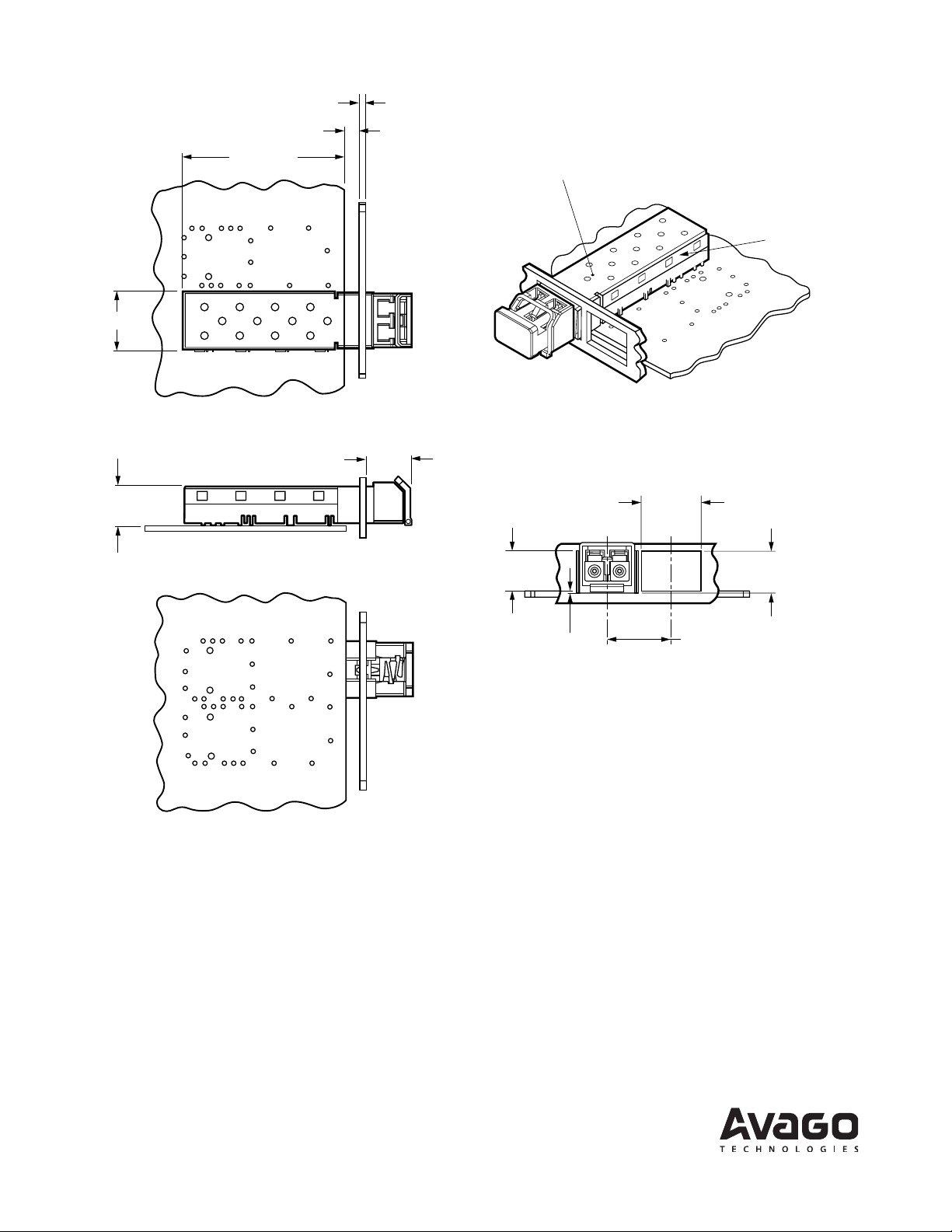
Figure 5. Module drawing
DEVICE SHOWN WITH
DUST CAP AND
BAIL DELATCH
AFBR-57J7APZ
850nm LASER PROD
21CRF(J) CLASS1
CHINA 0445
SN: A30445CD1C
A
F
B
R-57J
7A
P
Z
8
5
0
nm
L
AS
E
R
P
R
O
D
2
1
C
R
F
(
J
)
C
L
AS
S
1
C
H
I
N
A
0
4
4
5
S
N
:
A3
0
4
4
5
C
D
1
C
55.3 – 0.2
8.5 – 0.1
13.4 – 0.1
6.25 – 0.05
TX RX
1.91
13.6
12.4 – 0.2
13.6
14.9 UNCOMPRESSED
0.55 UNCOMPRESSED
1.39 UNCOMPRESSED
16

2x 1.7
20x 0.5 ± 0.03
0.9
2 ± 0.005 TYP.
0. 0 6 L A S B S
10.53
11.93
20
10
11
PIN 1
20
10
11
PIN 1
0.8
TYP .
10.93
9.6
2x 1.55 ± 0.05
3.2
5
LEGEND
1. PADS AND VIAS ARE CHASSIS GROUND
2. THROUGH HOLES, PLATING OPTIONAL
3. HATCHED AREA DENOTES COMPONENT
AND TRACE KEEPOUT (EXCEPT
CHASSIS GROUND)
4. AREA DENOTES COMPONENT
KEEPOUT (TRACES ALLOWED)
DIMENSIONS ARE IN MILLIMETERS
4
3
2
1
1
26.8
5
11x 2.0
10
3x
41.3
42.3
B
10x∅ 1.05 ± 0.01
16.25
REF .
14.25
11.08
8.58
5.68
2.0
11x
11.93
9.6
4.8
8.48
A
3.68
SEE DETAIL 1
9x 0.95 ± 0.05
2.5
7.17.2
2.5
10
3x
34.5
16.25
MIN. PITCH
Y
X
DET AIL 1
∅ 0.85 ± 0.05
PCB
EDGE
0. 0 6 L A S B S
∅ 0 .1 S
∅ 0 .1 L S
∅ 0 .1 L S
∅ 0.1 Y
S B
L A
X A
S X
X A
Figure 6. SFP host board mechanical layout
17
41.78 ±0.5
3.5 ± 0.3
1.7± 0.9
Tcase REFERENCE POINT
PCB
10 REF
(to PCB)
0.4± 0.1
(below PCB)
10.4 ± 0.1
15.25±0.1
16.25± 0.1 MIN. PITCH
DIMENSIONS ARE IN MILLIMETERS
11.73 REF
CAGE ASSEMBLY
9.8 MAX.
15 MAX.
Figure 7. SFP Assembly Drawing
For product information and a complete list of distributors, please go to our web site: www.avagotech.com
Avago, Avago Technologies, and the A logo are trademarks of Avago Technologies in the United States and other countries.
Data subject to change. Copyright © 2005-2009 Avago Technologies. All rights reserved.
AV02-1767EN - March 18, 2009
 Loading...