

ACPL-W60L/K63L
High Speed LVTTL Compa tible
3.3 V olt Optocouplers
Data Sheet
Description
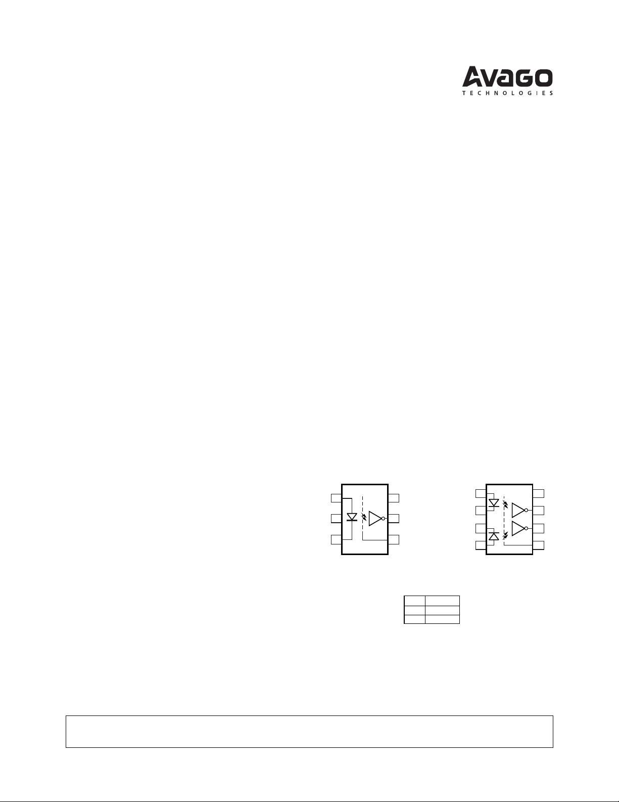
The ACPL-W60L/K63L are optically coupled gates
that combine a GaAsP light emitting diode and an
integrated high gain photo detector. The output of the
detector IC is an open collector Schottky-clamped
transistor. The internal shield provides a guaranteed
common mode transient immunity specification of 15
kV/µs.
This unique design provides maximum AC and DC
circuit isolation while achieving LVTTL/LVCMOS
compatibility. The optocoupler AC and DC operational
parameters are guaranteed from –40˚C to +85˚C
allowing trouble-free system performance.
Applications
• Isolated line receiver
• Computer-peripheral interfaces
• Microprocessor system interfaces
• Digital isolation for A/D, D/A conversion
• Switching power supply
• Instrument input/output isolation
• Ground loop elimination
• Pulse transformer replacement
• Fieldbus
CATHODE
Features
• Package clearance/creepage at 8 mm
• Low power consumption
• 15 kV/µs minimum Common Mode Rejection (CMR) at
VCM = 50 V
• High speed: 15 MBd typical
• LVTTL/LVCMOS compatible
• Low input current capability: 5 mA
• Guaranteed AC and DC performance over temperature:
–40˚C to +85˚C
• Available in 6-pin stretched SO-6 and 8 pin stretched
SO-8
• Safety approvals: UL, CSA, IEC/EN/DIN EN 60747-5-2 –
in process
Functional Diagram
ANODE
ACPL-W60L
1
2
3
SHIELD
V
6
CC
5
V
O
GND
4
ANODE
CATHODE
CATHODE
ANODE
1
1
2
2
ACPL-K63L
1
2
3
4
SHIELD
*
V
8
CC
V
7
O1
V
6
O2
GND
5
TRUTH TABLE
(POSITIVE LOGIC)
LED
OUTPUT
ON
OFF
L
H
*Advanced Information
A 0.1 µF bypass capacitor must be
connected between pins 5 and 8.
CAUTION: It is advised that normal static precautions be taken in handling and assembly of this component to prevent
damage and/or degradation which may be induced by ESD.
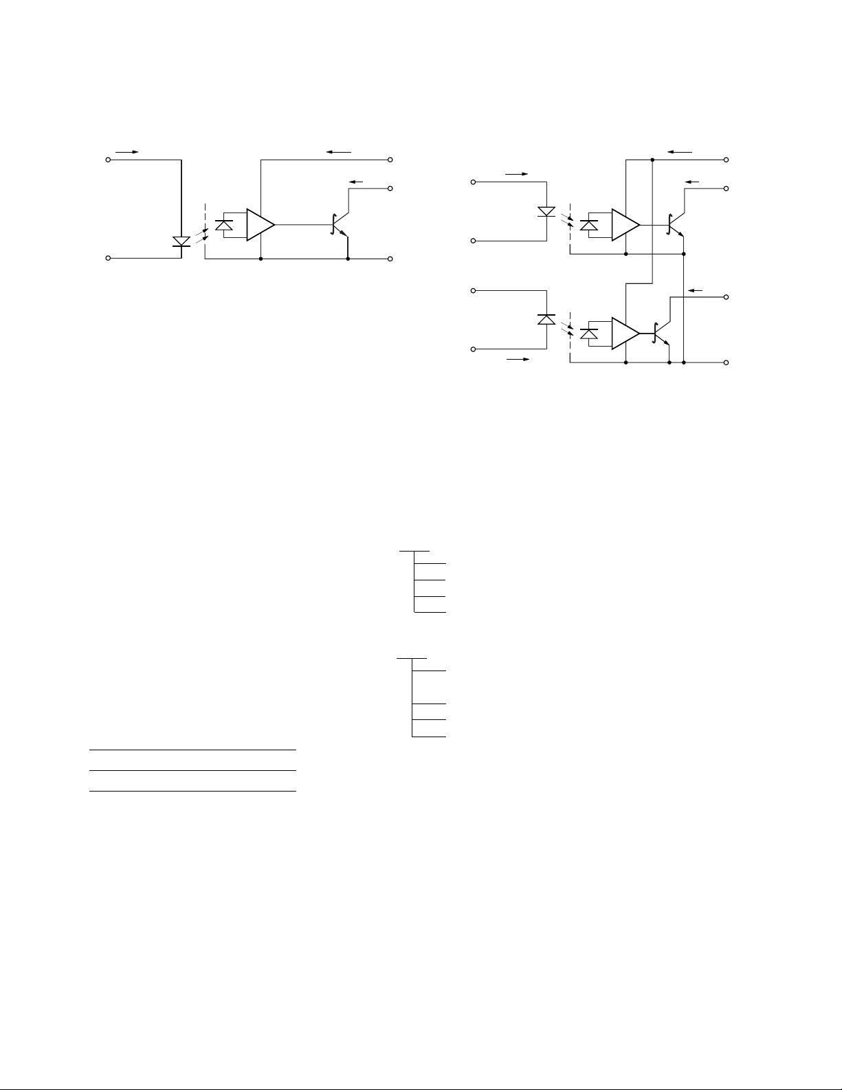
Schematic Diagrams
I
F
1+
V
F
–
3
USE OF A 0.1 µF BYPASS CAPACITOR CONNECTED
BETWEEN PINS 5 AND 8 IS RECOMMENDED (SEE NOTE 5).
These optocouplers are suitable
for high speed logic interfacing,
ACPL-W60L
SHIELD
Ordering Information
Specify Part Number followed by Option Number (if desired).
input/output buffering, as line
receivers in environments that
conventional line receivers
Example:
ACPL-W60L -XXXX
cannot tolerate and are
recommended for use in
extremely high ground or induced
noise environments.
Example:
These optocouplers are available
ACPL-K63L -XXXX*
in stretched SO-6 and SO-8
package. The part numbers are as
follows:
Package
ACPL-W60L Stretched SO-6
ACPL-K63L Stretched SO-8
Option data sheets available. Contact Avago sales representative or
authorized distributor for information.
I
CC
V
CC
6
I
O
V
O
5
GND
4
I
F1
1
+
V
F1
–
2
3
–
V
F2
+
I
4
F2
ACPL-K63L
SHIELD
SHIELD
I
CC
V
CC
8
I
O1
V
O1
7
I
O2
V
O2
6
GND
5
020 = UL5000 Vrms/minute Option
060 = IEC/EN/DIN EN 60747-5-2
500 = Tape and Reel Packaging Option
XXXE = Lead Free Option
020 = UL5000 Vrms/minute Option – pending
qualification
060 = IEC/EN/DIN EN 60747-5-2
500 = Tape and Reel Packaging Option
XXXE = Lead Free Option
2

Package Outline Drawings
ACPL-W60L Stretched SO-6 Package
0.381 ± 0.127
(0.015 ± 0.005)
0.45 (0.018)
1
2
3
6.807
0.268
(
7°
45°
1.27 (0.050) BSG
+0.127
0
+0.005
)
-0.000
6
5
4
1.590 ± 0.127
(0.063 ± 0.005)
4.580
0.180
(
+0.254
0
+0.010
-0.000
LAND PATTERN RECOMMENDATION
12.65 (0.498)
0.76 (0.030)
)
1.91 (0.075)
7°
0.20 ± 0.10
(0.008 ± 0.004)
0.750 ± 0.250
(0.0295 ± 0.010)
11.50 ± 0.250
(0.453 ± 0.010)
ACPL-K63L Stretched SO-8 Package
0.381 ± 0.13
(0.015 ± 0.005)
1
2
3
4
1.270 (0.050) BSG
8
7
6
5
3.180 ± 0.127
(0.125 ± 0.005)
+0.25
5.850
0
+0.010
0.230
(
-0.000
DIMENSIONS IN MILLIMETERS (INCHES).
LEAD COPLANARITY = 0.1 mm (0.004 INCHES).
LAND PATTERN RECOMMENDATION
12.650 (0.5)
)
0.450 (0.018)
0.200 ± 0.100
(0.008 ± 0.004)
0.750 ± 0.250
(0.0295 ± 0.010)
3
1.590 ± 0.127
7°
45°
6.807 ± 0.127
(0.268 ± 0.005)
11.5 ± 0.250
(0.453 ± 0.010)
(0.063 ± 0.005)
3.180 ± 0.127
(0.125 ± 0.005)
7°
DIMENSIONS IN MILLIMETERS (INCHES).
LEAD COPLANARITY = 0.1 mm (0.004 INCHES).
1.905 (0.1)
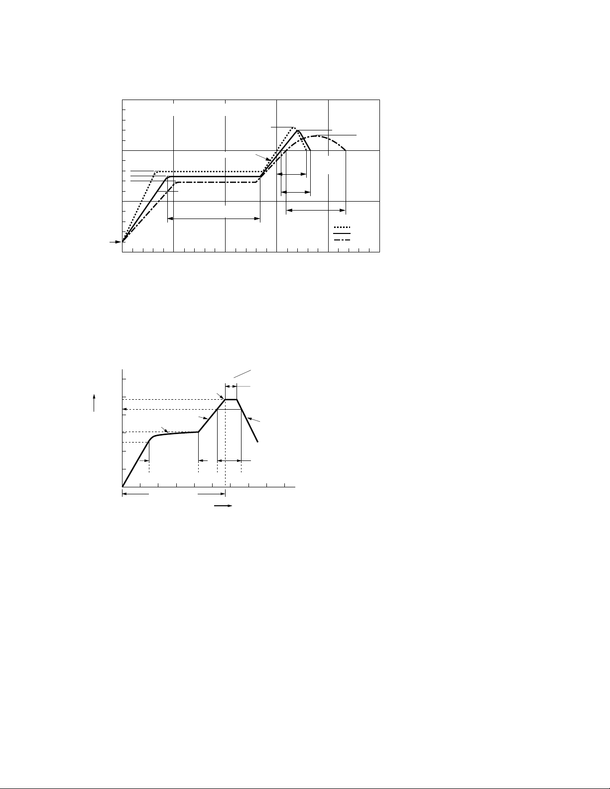
Recommended Solder Reflow Thermal Profile
300
PREHEATING RATE 3°C + 1°C/–0.5°C/SEC.
REFLOW HEATING RATE 2.5°C ± 0.5°C/SEC.
ROOM
TEMPERATURE
200
160°C
150°C
140°C
100
TEMPERATURE (°C)
0
0
50 150100 200 250
2.5°C ± 0.5°C/SEC.
3°C + 1°C/–0.5°C
PREHEATING TIME
150°C, 90 + 30 SEC.
TIME (SECONDS)
Note:
Use of non chlorine-activated fluxes is highly recommended.
Recommended PB-Free IR Profile
PEAK
TEMP.
245°C
30
SEC.
SEC.
30
SOLDERING
TIME
200°C
50 SEC.
PEAK
TEMP.
240°C
PEAK
TEMP.
230°C
TIGHT
TYPICAL
LOOSE
T
p
217 °C
T
L
150 - 200 °C
T
smax
T
smin
TEMPERATURE
25
NOTES:
THE TIME FROM 25 °C to PEAK TEMPERATURE = 8 MINUTES MAX.
T
= 200 °C, T
smax
t 25 °C to PEAK
260 +0/-5 °C
RAMP-UP
3 °C/SEC. MAX.
t
s
PREHEAT
60 to 180 SEC.
= 150 °C
smin
TIME
Note:
Use of non chlorine-activated fluxes is highly recommended.
Regulatory Information
The ACPL-W60L//K63L have
been approved by the following
organizations:
UL - Pending
Approval under UL 1577,
Component Recognition
Program, File E55361.
TIME WITHIN 5 °C of A CTUAL
PEAK TEMPERATURE
t
p
20-40 SEC.
RAMP-DOWN
6 °C/SEC. MAX.
t
L
60 to 150 SEC.
CSA - Pending
Approval under CSA Component
Acceptance Notice #5, File CA
88324.
IEC/EN/DIN EN 60747-5-2 - Pending
Approved under:
IEC 60747-5-2:1997 + A1:2002
EN 60747-5-2:2001 + A1:2002
DIN EN 60747-5-2 (VDE 0884
Teil 2):2003-01
(Option 060 only)
4
 Loading...