

Avago ACPL-785J Schematic [ru]

ACPL-785J
Lead (Pb) Free
RoHS 6 fully
compliant
RoHS 6 fully compliant options available;
-xxxE denotes a lead-free product
16
15
14
13
12
11
10
9
1
2
3
4
5
6
7
8
FAULT
ABSVAL
V
OUT
V
REF
V
IN+
V
IN-
R
SENSE1
SHORT CIRCUIT FAULT
ISOLATION BOUNDARY
A/D
CONVERTER
MICRO
CONTROLLER
ACPL-785J
16
15
14
13
12
11
10
9
1
2
3
4
5
6
7
8
FAULT
ABSVAL
V
OUT
V
REF
V
IN+
V
IN-
R
SENSE2
ISOLATION BOUNDARY
ACPL-785J
16
15
14
13
12
11
10
9
1
2
3
4
5
6
7
8
FAULT
ABSVAL
V
OUT
V
REF
V
IN+
V
IN-
R
SENSE3
ISOLATION BOUNDARY
ACPL-785J
M
+5 V
OVERLOAD
FAULT
+
–
+
–
3 PHASE ABSOLUTE
VALUE OUTPUT
V
REF
V
TH
3 PHASE
MOTOR
Isolation Amplifier with Short Circuit and Overload Detection
Data Sheet
Description
Avago’s Isolation Amplifier with Short Circuit and
Overload Detection makes motor phase current sensing
compact, affordable and easy-to-implement while satisfying worldwide safety and regulatory requirements.
Applications
• Motor phase and rail current sensing
• Power inverter current and voltage sensing
• Industrial process control
• Data acquisition systems
• General purpose current and voltage sensing
• Traditional current transducer replacements
Features
• Output Voltage Directly Compatible with A/D
Converters (0 V to V
• Fast (3 µs) Short Circuit Detection with Transient Fault
Rejection
• Absolute Value Signal Out put for Overload Detection
• 1 µV/°C Offset Change vs. Temperature
• SO-16 Package
• -40°C to +85°C Operating Temperature Range
• 25 kV/µs Isolation Transient Immunity
• Regulatory Approvals: UL, CSA, IEC/EN/DIN EN
60747-5-5 (891 Vpeak Working Voltage)
Low Cost Three Phase Current Sensing with Short Circuit and Overload Detection
REF
)
CAUTION: It is advised that normal static precautions be taken in handling and assembly of
this component to prevent damage and/or degradation which may be induced by ESD.
Description
16
15
14
13
12
11
10
9
1
2
3
4
5
6
7
8
GND
2
V
DD2
FAULT
ABSVAL
V
OUT
V
REF
V
DD2
GND
2
V
IN+
V
IN-
C
H
C
L
V
DD1
V
LED+
V
DD1
GND
1
R
SHUNT
0.02
ISOLATED +5 V
4.7 k
39
.01 F
0.1 F
0.1 F
ISOLATION BOUNDARY
INPUT
CURRENT
+5 V
A/D
V
REF
GND
C
TO OTHER
PHASE
OUTPUTS
+
0.1 F
ACPL-785J
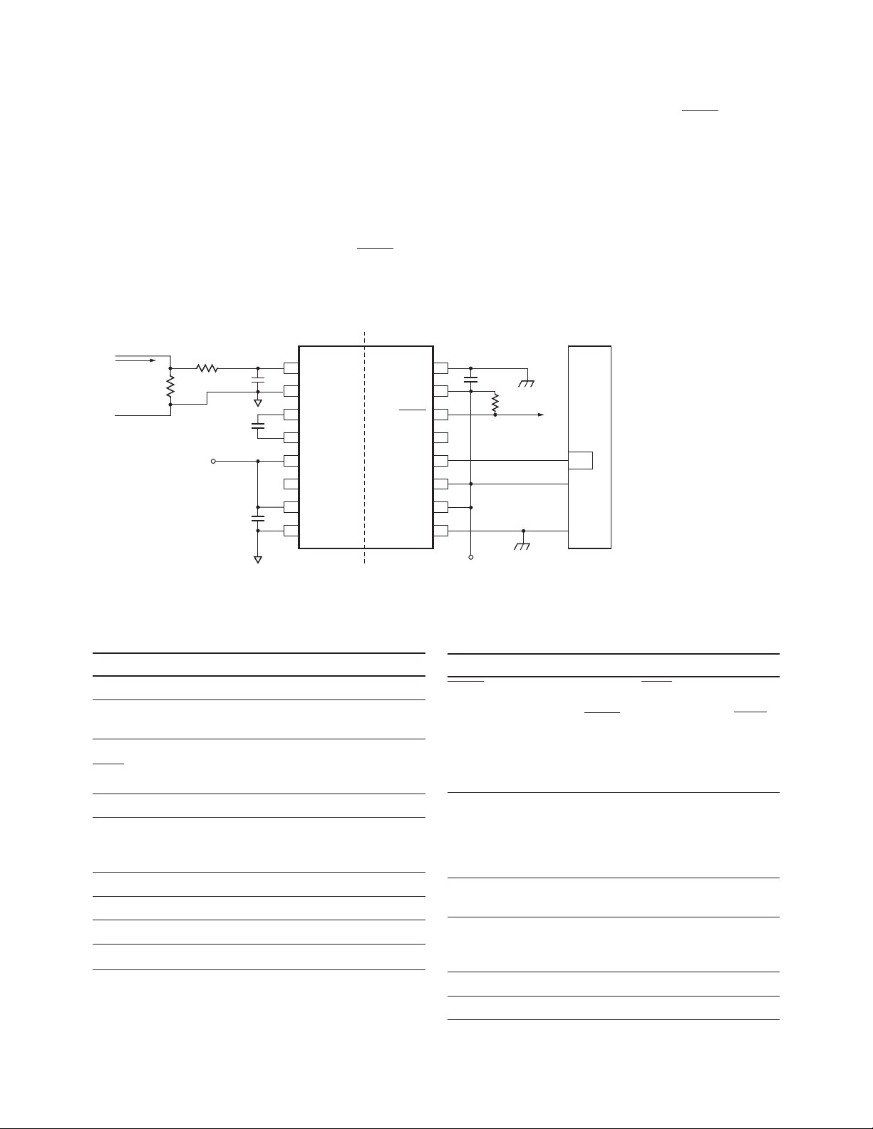
The ACPL-785J isolation amplifier is designed for current
sensing in electronic motor drives. In a typical implementation, motor currents flow through an external resistor
and the resulting analog voltage drop is sensed by the
ACPL-785J. A larger analog output voltage is created
on the other side of the ACPL-785J’s optical isolation
barrier. The output voltage is proportional to the motor
current and can be connected directly to a single-supply
A/D converter. A digital over-range output (FAULT) and
an analog rectified output (ABSVAL) are also provided.
The wire OR-able over-range output (FAULT) is useful
for quick detec tion of short circuit con ditions on any
of the motor phases. The wire-OR-able rectified output
(ABSVAL), simplifies measure-ment of motor load since
it performs polyphase rectification. Since the commonmode voltage swings several hundred volts in tens of
nanoseconds in modern electronic motor drives, the
ACPL-785J was designed to ignore very high commonmode transient slew rates (10 kV/µs).
Figure 1. Current sensing circuit.
Pin Descriptions
Symbol Description
V
Positive input voltage (±200 mV recommended).
IN+
V
Negative input voltage (normally connected to
IN-
GND1).
CH Internal Bias Node. Connections to or between CH
and CL other than the re quired 0.1 µF capacitor
C
L
shown, are not recommended.
V
Supply voltage input (4.5 V to 5.5 V).
DD1
V
LED anode. This pin must be left uncon nected for
LED+
guaranteed data sheet perfor mance. (For optical
coupling testing only.)
V
Supply voltage input (4.5 V to 5.5 V).
DD1
GND1 Ground input.
GND2 Ground input.
V
2
Supply voltage input (4.5 V to 5.5 V).
DD2
Symbol Description
FAULT Short circuit fault output. FAULT changes from a
high to low output voltage within 6 µs after
V
is an open drain output which allows outputs from
all the ACPL-785Js in a circuit to be connected
together (“wired-OR”) forming a single fault signal
for interfacing directly to the micro-controller.
ABSVAL Absolute value of V
when VIN=0 and increases toward V
approaches +256 mV or -256 mV. ABSVAL is
“wired-OR” able and is used for detecting
overloads.
V
Voltage output. Swings from 0 to V
OUT
The nominal gain is V
V
Reference voltage input (4.0 V to V
REF
voltage establishes the full scale output ranges
and gains of V
V
Supply voltage input (4.5 V to 5.5 V).
DD2
GND2 Ground input.
exceeds the FAULT Detection Threshold. FAULT
IN
output. ABSVAL is 0 V
OUT
/504 mV.
REF
and ABSVAL.
OUT
DD2
REF
.
REF
). This
as VIN
Ordering Information
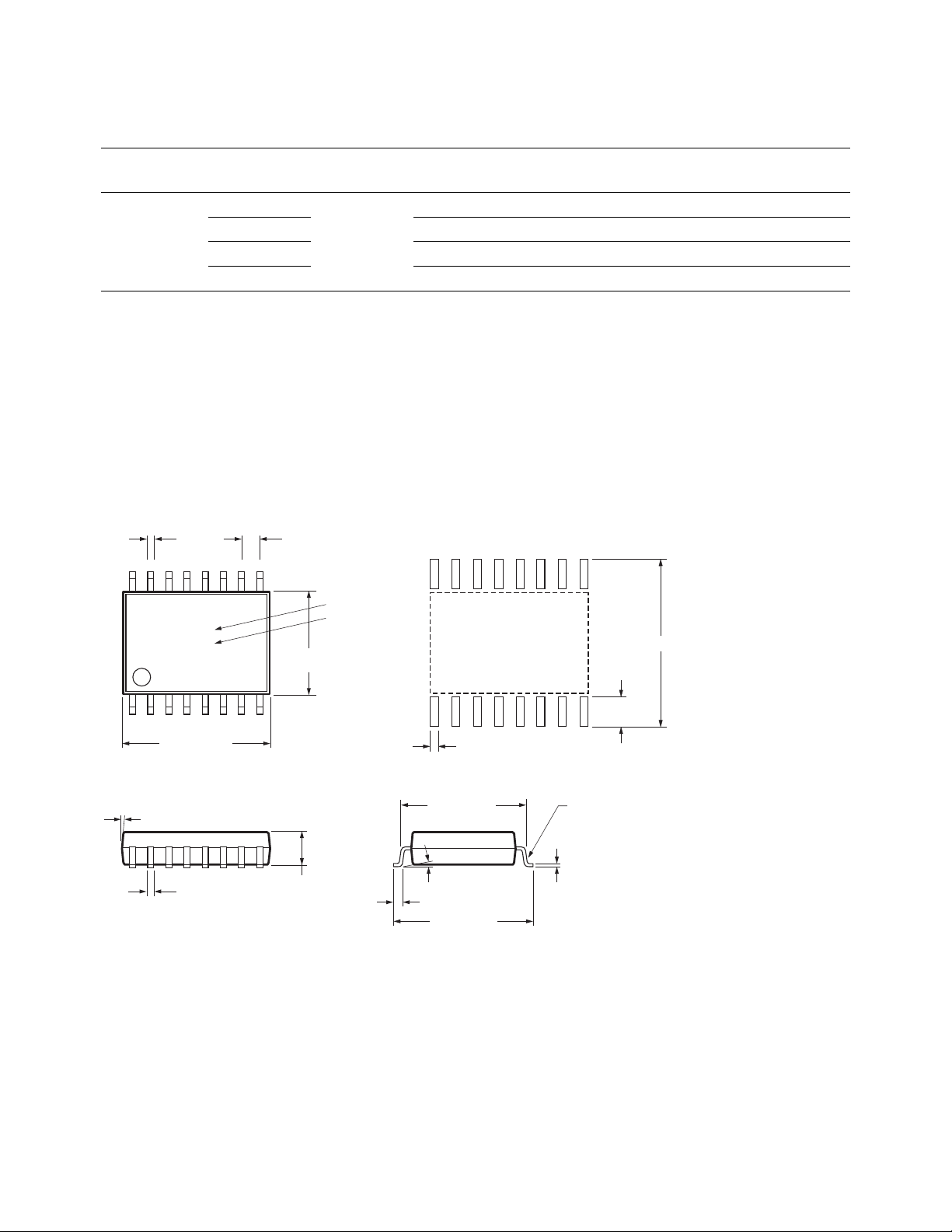
9
0.295 ± 0.010
(7.493 ± 0.254)
10111213141516
87654321
0.018
(0.457)
0.138 ± 0.005
(3.505 ± 0.127)
9°
0.406 ± 0.10
(10.312 ± 0.254)
0.408 ± 0.010
(10.160 ± 0.254)
0.025 MIN.
0.008 ± 0.003
(0.203 ± 0.076)
STANDOFF
0.345 ± 0.010
(8.986 ± 0.254)
0–8°
0.018
(0.457)
0.050
(1.270)
ALL LEADS
TO BE
COPLANAR
± 0.002
A 785J
YYWW
TYPE NUMBER
DATE CODE
0.458 (11.63)
0.085 (2.16)
0.025 (0.64)
LAND PATTERN RECOMMENDATION
ACPL-785J is UL Recognized with 3750 Vrms for 1 minute per UL1577.
Part number
ACPL-785J
Option (RoHS
Compliant) Package Surface Mount Tape & Reel
-000E
-060E X X 45 per tube
SO-16
X 45 per tube
IEC/EN/DIN EN
60747-5-5 Quantity
-500E X X 850 per reel
-560E X X X 850 per reel
To order, choose a part number from the part number column and combine with the desired option from the option
column to form an order entry.
Example:
ACPL-785J-560E to order product of 16-Lead Surface Mount package in Tape and Reel packaging with IEC/EN/DIN EN
60747-5-5 Safety Approval and RoHS compliant.
Package Outline Drawings
16-Lead Surface Mount
Dimensions in inches (millimeters)
3
Note: Initial and continued variation in the color of the white mold
compound is normal and does not affect device performance or
reliability.
Note: Floating lead protrusion is 0.25 mm (10 mils) max.

Package Characteristics
Parameter Symbol Min. Typ. Max. Units Test Conditions Fig. Notes
Input-Output Momentary
Withstand Voltage
Resistance (Input-Output) R
Capacitance (Input-Output) C
Input IC Junction-to-Case
Thermal Resistance
Output IC Junction-to-Case
Thermal Resistance
V
ISO
I-O
I-O
θjci
θjco
3750 Vrms RH < 50%, t = 1 min.,
TA = 25°C
9
>10
Ω
V
I-O
= 500 V
DC
1.3 pF f = 1 MHz 3
120 °C/W TA = 85°C
100 °C/W TA = 85°C
1,2,3
3
Recommended Pb-Free IR Profile
Recommended reflow condition as per JEDEC Standard,
J-STD-020 (latest revision). Non-Halide Flux should be
used.
Regulatory Information
The ACPL-785J is pending for approvals by the following organizations:
IEC/EN/DIN EN 60747-5-5
Approved with Maximum Working Insulation Voltage
V
IORM
= 891 V
peak
.
UL
Approval under UL 1577, component recognition
program up to V
= 3750 Vrms/1min. File E55361.
ISO
CSA
Approval under CSA Component Acceptance Notice #5,
File CA 88324
4

IEC/EN/DIN EN 60747-5-5 Insulation Characteristics*
P
s
– POWER – mW
0
0
TS – CASE TEMPERATURE – °C
20025
800
50 75 100
200
150 175125
400
600
Psi – OUTPUT
Psi – INPUT
Description Symbol Characteristic Unit
Installation classification per DIN VDE 0110/1.89, Table 1
for rated mains voltage ≤ 300 V
for rated mains voltage ≤ 300 V
for rated mains voltage ≤ 600 V
rms
rms
rms
Climatic Classification 55/85/21
Pollution Degree (DIN VDE 0110/1.89) 2
Maximum Working Insulation Voltage V
Input to Output Test Voltage, Method b**
V
x 1.875 = VPR, 100% Production Test with
IORM
tm = 1 sec, Partial discharge < 5 pC
Input to Output Test Voltage, Method a**
V
x 1.6 = VPR, Type and Sample Test, tm = 10 sec,
IORM
Partial discharge < 5 pC
Highest Allowable Overvoltage (Transient Overvoltage t
= 60 sec) V
ini
IORM
V
PR
V
PR
IOTM
Safety-limiting values — maximum values allowed in the
event of a failure, also see Figure 2.
Case Temperature
Input Power
Output Power
Insulation Resistance at T
* Isolation characteristics are guaranteed only within the safety maximum ratings which must be ensured by protective circuits within the
application. Surface Mount Classification is class A in accordance with CECC00802.
** Refer to the optocoupler section of the isolation and Control Components Designer’s Catalog, under Product Safety Regulations section IEC/EN/
DIN EN 6747-5-5, for a detailed description of Method a and Method b partial discharge test profiles.
= 500 V R
SI, VIO
T
S
P
S1, INPUT
P
S1, OUTPUT
S
I-IV
I-III
I-II
891 V
1670 V
1425 V
6000 V
175
400
600
9
>10
PEAK
PEAK
PEAK
PEAK
°C
mW
mW
Ω
Figure 2. Dependence of safety-limiting values on temperature.
5

Insulation and Safety Related Specifications
Parameter Symbol Min. Max. Conditions
Minimum External Air Gap
(Clearance)
Minimum External Tracking
(Creepage)
Minimum Internal Plastic Gap 0.5 mm Through insulation distance conductor to conductor,
Tracking Resistance CTI >175 Volts DIN IEC 112/VDE 0303 Part 1
Isolation Group IIIa Material Group (DIN VDE 0110, 1/89, Table 1)
L(101) 8.3 mm Measured from input terminals to output terminals,
shortest distance through air.
L(102) 8.3 mm Measured from input terminals to output terminals,
shortest distance path along body.
usually the straight line distance thickness between the
emitter and detector.
Comparative Tracking Index)
Absolute Maximum Ratings
Parameter Symbol Min. Max. Units Note
Storage Temperature T
Operating Temperature T
Supply Voltages V
Steady-State Input Voltage V
2 Second Transient Input Voltage V
Output Voltage V
S
A
DD1
IN+
IN+
OUT
, V
, V
, V
DD2
IN-
IN-
Absolute Value Output Voltage ABSVAL -0.5 V
Reference Input Voltage V
Reference Input Current I
Output Current I
Absolute Value Current I
FAULT Output Current I
Input IC Power Dissipation P
Output IC Power Dissipation P
REF
REF
VOUT
ABSVAL
FAU LT
I
O
-55 125 °C
-40 100 °C
0.0 5.5 V 4
-2.0 V
-6.0 V
-0.5 V
0 V
+ 0.5 V
DD1
+ 0.5 V
DD1
+ 0.5 V
DD2
+ 0.5 V
DD2
+ 0.5 V V 5
DD2
20 mA
20 mA
20 mA
20 mA
200 mW
200 mW
Recommended Operating Conditions
Parameter Symbol Min. Max. Units Note
Ambient Operating Temperature T
Supply Voltages V
Input Voltage (accurate and linear) V
Input Voltage (functional) V
Reference Input Voltage V
FAULT Output Current I
6
A
DD1
IN+
IN+
REF
FAU LT
, V
, V
, V
DD2
IN-
IN-
-40 85 °C
4.5 5.5 V
-200 200 mV
-2 2 V
4.0 V
DD2
V
4 mA

DC Electrical Specifications
Unless otherwise noted, all typicals and figures are at the nominal operating conditions of V
4.0 V, V
DD1
= V
= 5 V and TA = 25°C; all Minimum/Maximum specifications are within the Recommended Operating
DD2
Conditions.
Test
Parameter Symbol Min. Typ. Max. Units
Input Offset
Voltage
Magnitude of Input
Offset Change vs.
Temperature
V
Gain G V
OUT
Magnitude of V
Gain Change vs.
OUT
Temperature
V
200 mV
OUT
Nonlinearity
Maximum Input
Voltage Before
V
Clipping
OUT
FAULT Detection
Threshold
FAULT Low
Output Voltage
FAULT High
Output Current
ABSVAL Output
Error
Input Supply
Current
Output Supply
Current
Reference Voltage
Input Current
Input Current I
Input Resistance R
V
Output
OUT
Resistance
ABSVAL Output
Resistance
Input DC CommonMode Rejection
Ratio
V
OS
|∆VOS/∆TA|
|∆G/∆TA|
NL
200
|V
IN+|MAX
|V
| 230 256 280 mV 10 9
THF
V
OLF
I
OHF
e
ABS
-3 0 3 mV V
/504
REF
mV - 5%
1 10
V
/504 mVV
REF
/504
REF
mV + 5%
µV/°C
V/V |V
50 300 ppm/°C |V
0.06 0.4 % |V
256 mV
350 800 mV IOL = 4 mA
0.2 15
µA
0.6 2 % of
full scale
output
I
DD1
I
DD2
I
VREF
IN+
IN
R
OUT
R
ABS
CMRR
IN
10.7 20 mA
10.4 20 mA
0.26 1 mA
-350 nA V
800
0.2
0.3
kΩ
Ω
Ω
85 dB 11
Conditions Fig. Note
= 0 V,
IN+
TA = –40°C to +85°C
V
= 0 V,
IN+
TA = –40°C to +85°C
| < 200 mV,
IN+
TA = 25°C
| < 200 mV,
IN+
TA = 25°C
| < 200 mV,
IN+
TA = –40°C to +85°C
V
= V
FAU LT
DD2
= 0 V
IN+
V
= 0 V
IN+
= 0, V
IN+
= 0 V, V
IN-
3, 4,
6
5
7
6,7,
8,9
6,7,
8,9
6,7,
8,9
11 10
=
REF
8
7
 Loading...