

ACPL-061L, ACPL-064L, ACPL-M61L,
ACPL-W61L, ACPL-K64L
Ultra Low Power 10 MBd Digital CMOS Optocouplers
Data Sheet
Lead (Pb) Free
RoHS 6 fully
compliant
RoHS 6 fully compliant options available;
-xxxE denotes a lead-free product
Description
The Avago ultra low power ACPL-x6xL digital optocouplers
combine an AlGaAs light emitting diode (LED) and an
integrated high gain photodetector. The optocoupler
consumes extremely low power, at maximum 1.3mA I
current per channel across temperature. With a forward
LED current as low as 1.6 mA most microprocessors can
directly drive the LED.
An internal Faraday shield provides a guaranteed common
mode transient immunity specification of 20 kV/Ps.
Maximum AC and DC circuit isolation is achieved while
maintaining TTL/CMOS compatibility.
The optocouplers CMOS outputs are slew-rate controlled
and is designed to allow the rise and fall time to be controlled over a wide load capacitance range.
The ACPL-x6xL series operates from both 3.3 V and 5 V
supply voltages with guaranteed AC and DC performance
from –40°C to +105°C.
These low-power optocouplers are suitable for high speed
logic interface applications.
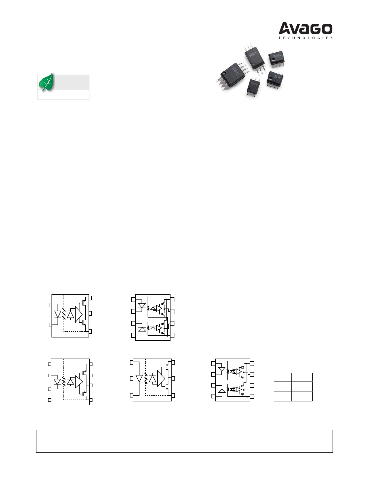
Functional Diagrams
Anode
Cathode
ACPL-M61L
1
3
6
V
DD
5
Vo
Anode1
Cathode1
Cathode2
4
GND
Anode2
ACPL-064L
1
2
3
4
SHIELD
Features
x Ultra-low IDD current: 1.3 mA/channel maximum
x Low input current: 1.6 mA
x Built-in slew-rate controlled outputs
DD2
x 20 kV/Ps minimum Common Mode Rejection (CMR) at
V
= 1000 V
CM
x High speed: 10 MBd minimum
x Guaranteed AC and DC performance over wide
temperature: –40°C to +105°C
x Wide package selection: SO-5, SO-8, stretched SO-6
and stretched SO-8
x Safety approval
– UL 1577 recognized – 3750 Vrms for 1 minute for
ACPL-061L/064L/M61L and 5000 Vrms* for 1 minute
for ACPL-W61L/K64L
– CSA Approval
– IEC/EN/DIN EN 60747-5-5 approval for Reinforced
Insulation (approved for ACPL-M61L, pending
approval for ACPL-064L/W61L/K64L/061L)
x RoHS compliant
Applications
x Communication interfaces: RS485, CANBus and I2C
8
V
DD
x Microprocessor system interfaces
7
Vo
1
x Digital isolation for A/D and D/A convertors
6
Vo
2
GND
5
NC
Anode
Cathode
NC
ACPL-061L^
1
2
3
8
V
DD
7
NC
6
Vo
Preliminary Information
4
SHIELD
* Pin 7 of the ACPL-061L is not connected
A 0.1
PF bypass capacitor must be connected betwee
^ Advanced information, may subject to changes.
5
GND
CAUTION: It is advised that normal static precautions be taken in handling and assembly
of this component to prevent damage and/or degradation which may be induced by ESD.
Anode
NC*
Cathode
ACPL-W61L
1
2
3
SHIELD
n pins VDD and GND.
ACPL-K64L
6
V
DD
5
Cathode1
Vo
Cathode2
4
GND
Anode1
Anode2
1
2
3
4
SHIELD
8
V
7
Vo
6
Vo
GND
5
DD
1
2
TRUTH TABLE
(POSITIVE LOGIC)
LED OUTPUT
ON L
OFF H

Ordering Information
The ACPL-061L, ACPL-064L and ACPL-M61L are UL Recognized with an isolation voltage of 3750 V
UL1577. The ACPL-W61L and ACPL-K64L are UL Recognized with an isolation voltage of 5000 V
for 1 minute per
rms
for 1 minute per
rms
UL1577. All devices are RoHS compliant.
Option
RoHS
Part number
ACPL-061L
ACPL-064L -000E SO-8 X 100 per tube
ACPL-M61L -000E SO-5 X 100 per tube
ACPL-W61L -000E Stretched
ACPL-K64L -000E Stretched
^
Compliant
-000E SO-8 X 100 per tube
-500E X X 1500 per reel
-560E X X X 1500 per reel
-500E X X 1500 per reel
-560E X X X 1500 per reel
-500E X X 1500 per reel
-560E X X X 1500 per reel
-500E X X X 1000 per reel
-560E XXXX1000 per reel
-500E X X X 1000 per reel
-560E XXXX1000 per reel
Package Surface Mount
X X 100 per tube
S06
X X 80 per tube
S08
Tape
& Reel
UL 5000 V
1 Minute
rating
rms
/
IEC/EN/
DIN EN
60747-5-5 Quantity
To form an ordering part number, choose a part number from the part number column and combine it with the desired
option from the option column.
Example 1:
The part number ACPL-M61L-560E describes an optocoupler with a surface mount SO-5 package; delivered in Tape and
Reel with 1500 parts per reel; with IEC/EN/DIN EN 60747-5-5 Safety Approval; and full RoHS compliance.
Option datasheets are available. Contact your Avago sales representative or authorized distributor for information.
^ Advanced information, may subject to changes.
2
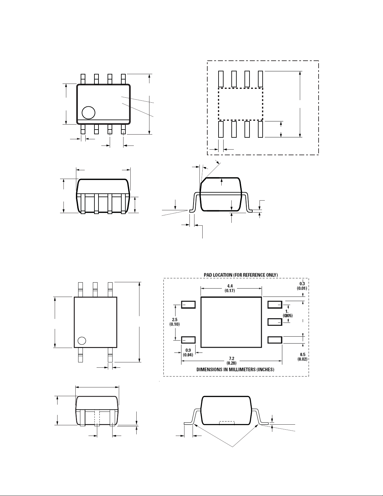
Package Outline Drawings
ACPL-061L and ACPL-064L SO-8 Package
8765
3.937 ± 0.127
(0.155 ± 0.005)
PIN ONE
0.406 ± 0.076
(0.016 ± 0.003)
*
(0.200 ± 0.005)
3.175 ± 0.127
(0.125 ± 0.005)
Total package length (inclusive of mold flash)
*
5.207 ± 0.254 (0.205 ± 0.010)
Dimensions in Millimeters (Inches).
Lead coplanarity = 0.10 mm (0.004 inches) max.
Option number 500 not marked.
Note: Floating lead protrusion is 0.15 mm (6 mils) max.
XXXV
YWW
4321
1.270
(0.050)
5.080 ± 0.127
5.994 ± 0.203
(0.236 ± 0.008)
TYPE NUMBER
(LAST 3 DIGITS)
DATE CODE
BSC
1.524
(0.060)
0 ~ 7°
7°
LAND PATTERN RECOMMENDATION
0.64 (0.025)
0.432
45° X
(0.017)
0.203 ± 0.102
(0.008 ± 0.004)
0.305
MIN.
(0.012)
7.49 (0.295)
1.9 (0.075)
0.228 ± 0.025
(0.009 ± 0.001)
ACPL-M61L SO-5 Package
4.4 ± 0.1
(0.173 ± 0.004)
2.5 ± 0.1
(0.098 ± 0.004)
1.27
(0.050)
Dimensions in Millimeters (Inches)
* Maximum mold flash on each side is 0.15 mm (0.006)
Note: Floating lead protrusion is 0.15 mm (6 mils) max.
3
XXX
3.6 ± 0.1*
(0.142 ± 0.004)
BSC
MXXX
7.0 ± 0.2
(0.276 ± 0.008)
0.4 ± 0.05
(0.016 ± 0.002)
0.102 ± 0.102
(0.004 ± 0.004)
0.71
(0.028)
MIN
(0.0085 ± 0.0015)
MAX. LEAD COPLANARITY
= 0.102 (0.004)
0.216 ± 0.038
7° MAX.
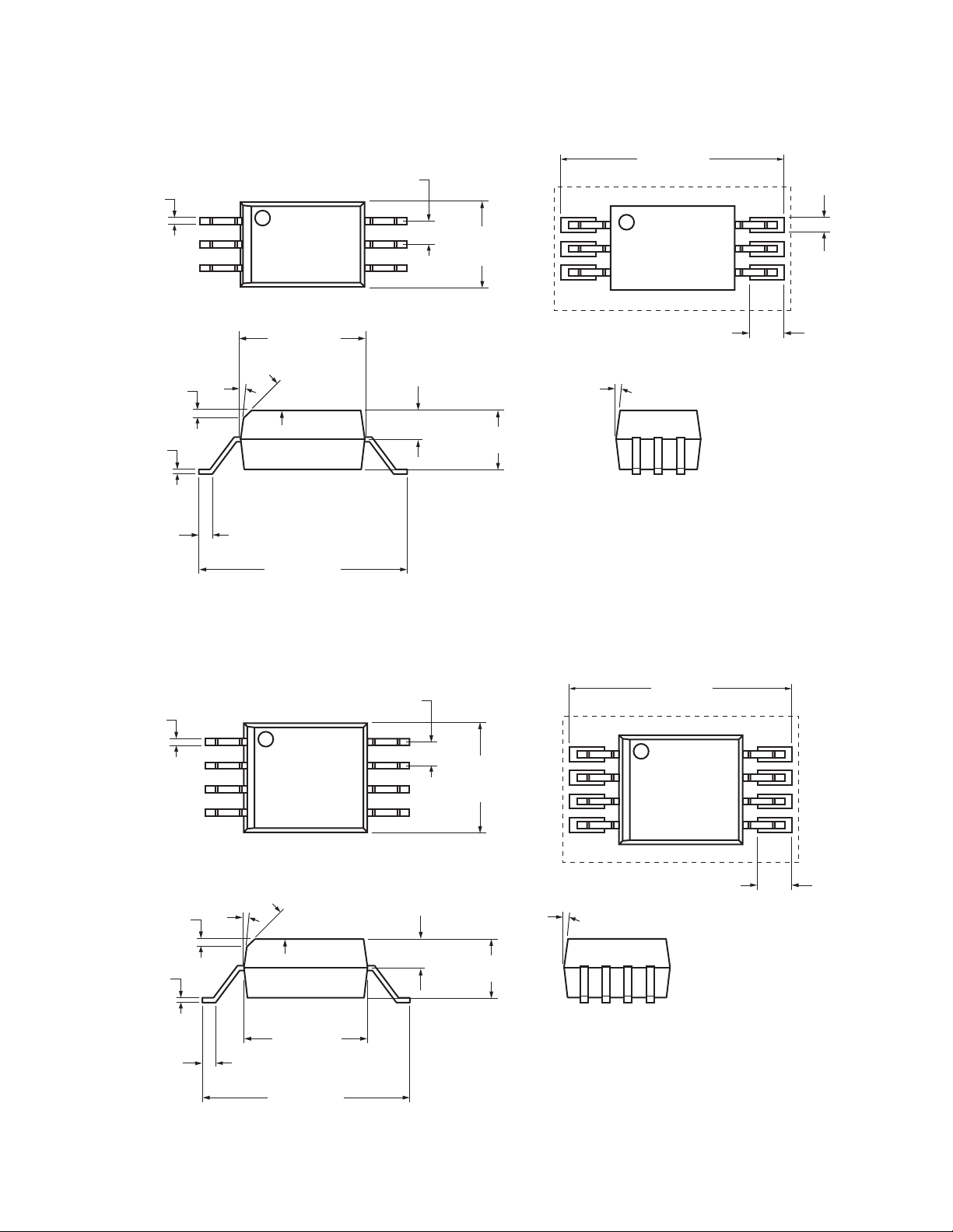
ACPL-W61L Stretched SO-6 Package
0.381 0.127
(0.015 0.005)
0.45 (0.018)
1
2
3
6.807
0.268
7°
45°
+0.127
0
+0.005
- 0.000
1.27 (0.050) BSG
6
5
4
)(
1.590 0.127
(0.063 0.005)
4.580
(
0.180
+0.254
0
+0.010
- 0.000
LAND PATTERN RECOMMENDATION
12.65 (0.498)
0.76 (0.030)
)
1.91 (0.075)
7°
0.20 0.10
(0.008 0.004)
0.750 0.250
(0.0295 0.010)
11.50 0.250
(0.453 0.010)
ACPL-K63L Stretched SO-8 Package
0.381 0.13
(0.015 0.005)
0.450 (0.018)
1
2
3
4
7°
45°
1.270 (0.050) BSG
8
7
6
5
1.590 0.127
(0.063 0.005)
3.180 0.127
(0.125 0.005)
+0.25
5.850
0
+0.010
(
0.230
- 0.000
Dimensions in Millimeters (Inches).
Lead coplanarity = 0.1 mm (0.004 inches).
LAND PATTERN RECOMMENDATION
12.650 (0.5)
)
1.905 (0.1)
7°
0.200 0.100
(0.008 0.004)
0.750 0.250
(0.0295 0.010)
4
6.807 0.127
(0.268 0.005)
11.5 0.250
(0.453 0.010)
3.180 0.127
(0.125 0.005)
Dimensions in Millimeters (Inches).
Lead coplanarity = 0.1 mm (0.004 inches).

Reflow Soldering Profile
The recommended reflow soldering conditions are per JEDEC Standard J-STD-020 (latest revision). Non-halide flux
should be used.
Regulatory Information
The ACPL-061L, ACPL-064L, ACPL-M61L, ACPL-W61L and ACPL-K64L are pending approval by the following organizations:
IEC/EN/DIN EN 60747-5-5 (Option 060 only)
UL
Approval under UL 1577 component recognition program up to V
V
= 5000 V
ISO
for the ACPL-W61L/K64L, File E55361.
RMS
CSA
Approval under CSA Component Acceptance Notice #5, File CA 88324.
Insulation and Safety Related Specifications
= 3750 V
ISO
for the ACPL-M61L/061L/064L and
RMS
ACPL-061L
Parameter Symbol
Minimum External
Air Gap
(External Clearance)
Minimum External
Tracking
(External Creepage)
Minimum Internal
Plastic Gap
(Internal Clearance)
Tracking Resistance
(Comparative Tracking
Index)
Isolation Group IIIa IIIa IIIa Material Group
L(101) 4.9 5 8 mm Measured from input terminals to
L(102) 4.8 5 8 mm Measured from input terminals to
CTI 175 175 175 V DIN IEC 112/VDE 0303 Part 1
ACPL-064L ACPL-M61L
0.08 0.08 0.08 mm Through insulation distance
ACPL-W61L
ACPL-K64L Units Conditions
output terminals, shortest distance
through air.
output terminals, shortest distance
path along body.
conductor to conductor, usually
the straight line distance thickness
between the emitter and detector.
(DIN VDE 0110, 1/89, Table 1)
5

IEC/EN/DIN EN 60747-5-5 Insulation Characteristics* (Option 060)
Characteristic
ACPL-061L^/
ACPL- 064L/
Description Symbol
Installation classification per DIN VDE 0110/39, Table 1
for rated mains voltage ≤ 150 V
for rated mains voltage ≤ 300 V
for rated mains voltage ≤ 600 V
for rated mains voltage ≤ 100 V
Climatic Classification 55/105/21 55/105/21
Pollution Degree (DIN VDE 0110/39) 2 2
Maximum Working Insulation Voltage V
Input to Output Test Voltage, Method b*
V
x 1.875=VPR, 100% Production Test with tm =1 sec,
IORM
Partial discharge < 5 pC
Input to Output Test Voltage, Method a*
V
x 1.6=VPR, Type and Sample Test, tm = 10 sec,
IORM
Partial discharge < 5 pC
Highest Allowable Overvoltage (Transient Overvoltage t
Safety-limiting values – maximum values allowed in the event of a failure.
Case Temperature
Input Current**
Output Power**
Insulation Resistance at T
* Refer to the optocoupler section of the Isolation and Control Components Designer’s Catalog, under Product Safety Regulations section, (IEC/EN/
DIN EN 60747-5-5) for a detailed description of Method a and Method b partial discharge test profiles.
** Refer to the following figure for dependence of PS and IS on ambient temperature.
, VIO = 500 V R
S
rms
rms
rms
rms
= 60 sec) V
ini
IORM
V
PR
V
PR
IOTM
T
S
I
S, INPUT
P
S, OUTPUT
S
ACPL- M61L
I – IV
I – III
I – II
560 1140 V
1063 2137 V
896 1824 V
6000 8000 V
150
150
600
9
>10
ACPL-W61L/
ACPL- K64L
I – IV
I – IV
I – III
I – III
175
230
600
9
>10
Unit
peak
peak
peak
peak
°C
mA
mW
:
Absolute Maximum Ratings
Parameter Symbol Min Max Units Condition
Storage Temperature T
Operating Temperature T
Reverse Input Voltage V
Supply Voltage V
Average Forward Input Current I
Peak Forward Input Current
S
A
R
DD
F
I
F(TRAN)
(IF at 1 Ps pulse width, <10% duty cycle)
Output Current I
Output Voltage V
Input Power Dissipation P
Output Power Dissipation P
Lead Solder Temperature T
O
O
I
O
LS
Solder Reflow Temperature Profile See Package Outline Drawings section
-55 125 °C
-40 105 °C
5V
6.5 V
–8 mA
–1 A
≤1 Ps Pulse Width,
<300 pulses per second
80 mA ≤1 Ps Pulse Width,
<10% Duty Cycle
10 mA
–0.5 VDD +0.5 V
14 mW
20 mW
260°C for 10 sec., 1.6 mm below seating plane
6

Recommended Operating Conditions
Parameter Symbol Min Max Units
Operating Temperature T
Input Current, Low Level I
Input Current, High Level I
Power Supply Voltage V
Forward Input Voltage V
Logic Low Input Voltage V
A
FL
FH
DD
F (OFF)
IL
- 40 105 °C
0 250 PA
1.6 6.0 mA
2.7 5.5 V
0.8 V
0 0.8 V
Electrical Specifications (DC)
Over the recommended temperature (TA = –40°C to +105°C) and supply voltage (2.7 V ≤ VDD ≤ 5.5 V). All typical specifications are at V
Parameter Symbol Min Typ Max Units Test Conditions
Input Forward Voltage V
Input Reverse
Breakdown Voltage
Logic High Output Voltage V
Logic Low Output Voltage V
Input Threshold Current I
Logic Low Output Supply
Current
Logic High Output Supply
Current
Input Capacitance C
Input Diode Temperature
Coefficient
= 5 V and TA = 25°C.
DD
BV
TH
I
DDL
I
DDH
'V
F
OH
OL
IN
R
F
/'T
0.95 1.3 1.7 V IF = 2 mA
35 VI
VDD - 0.1 V
VDD - 1.0 V
DD
DD
VI
VI
0.03 0.1 V IF = 2 mA, VI = 5 V (RT = 1.68 k:) or
0.18 0.4 V I
0.7 1.3 mA
0.8 1.3 mA
0.8 1.3 mA
60 pF f = 1 MHz, VF = 0 V
A
-1.6 mV/°C IF = 2 mA
= 10 PA
R
= 0 mA, VI = 0 V (RT = 1.68 k:) or
F
(RT = 870 :), IO = -20 PA
Figure 11
= 0 mA, VI = 0 V (RT = 1.68 k:) or
F
(RT = 870 :), IO = -3.2 mA
Figure 11
VI = 3.3V (RT = 870 :), IO = 20 PA
Figure 11
= 2 mA, VI = 5 V (RT = 1.68 k:) or
F
VI = 3.3V (RT = 870 :), IO = 3.2 mA
Figure 11
7

Switching Specifications (AC)
Over the recommended temperature (TA = –40°C to +105°C) and supply voltage (2.7 V ≤ VDD ≤ 5.5 V). All typical specifications are at V
Parameter Symbol Min Typ Max Units Test Conditions
Propagation Delay Time
to Logic Low Output
Propagation Delay Time
to Logic High Output
Pulse Width t
Pulse Width Distortion
Propagation Delay Skew
Output Rise Time
(10% – 90%)
Output Fall Time
(90% - 10%)
Static Common Mode
Transient Immunity at
Logic High Output
Static Common Mode
Transient Immunity at
Logic Low Output
Dynamic Common Mode
Transient Immunity
= 5 V, TA = 25°C.
DD
[1]
[1]
[2]
[3]
[4]
[5]
[6]
t
PHL
t
PLH
PW
100 ns
PWD 6 30 ns
t
PSK
t
R
46 80 ns IF = 2 mA, VI = 5 V, RT = 1.68 k:,
C
= 15 pF, CMOS Signal Levels.
L
40 80 ns
IF = 2 mA, VI = 3.3 V, RT = 870 :,
CL = 15 pF, CMOS Signal Levels.
Figure 11
30 ns
12 ns IF = 2 mA, VI = 5 V, RT = 1.68 k:,
CL = 15 pF, CMOS Signal Levels.
Figure 11
10 ns IF = 2 mA, VI = 3.3 V, RT = 870 :,
= 15 pF, CMOS Signal Levels.
C
L
Figure 11
t
F
12 ns IF = 2 mA, VI = 5 V, RT = 1.68 k:,
CL = 15 pF, CMOS Signal Levels.
Figure 11
10 ns I
= 2 mA, VI = 3.3 V, RT = 870 :,
F
C
= 15 pF, CMOS Signal Levels.
L
Figure 11
| CMH | 20 35 kV/PsVCM = 1000 V, TA = 25°C, IF = 0 mA,
V
= 0 V (RT =1.68 k:) or (RT = 870:),
I
CL = 15 pF, CMOS Signal Levels.
Figure 11
| CML | 20 35 kV/PsVCM = 1000 V, TA = 25°C, VI = 5 V
(RT = 1.68 k:) or VI = 3.3 V
(R
= 870:), IF = 2 mA, CL= 15 pF,
T
CMOS Signal Levels.
Figure 11
CMR
D
35 kV/PsVCM = 1000 V, TA = 25°C, IF = 2 mA,
= 5 V (RT = 1.68 k:) or VI = 3.3 V
V
I
(R
= 870:), 10MBd datarate, the
T
absolute increase of PWD < 10ns
Figure 11
8

Package Characteristics
All typicals are at TA = 25°C.
Parameter Symbol Part Number Min Typ Max Units Test Conditions
Input-Output Insulation V
Input-Output Resistance R
Input-Output Capacitance C
^ Advanced information, may subject to changes.
Notes:
1. t
propagation delay is measured from the 50% (Vin or IF) on the rising edge of the input pulse to the 50% VDD of the falling edge of the VO signal.
PHL
t
propagation delay is measured from the 50% (Vin or IF) on the falling edge of the input pulse to the 50% level of the rising edge of the VO
PLH
signal.
2. PWD is defined as |t
3. t
is equal to the magnitude of the worst case difference in t
PSK
recommended operating conditions.
4. CMH is the maximum tolerable rate of rise of the common mode voltage to assure that the output will remain in a high logic state.
5. CML is the maximum tolerable rate of fall of the common mode voltage to assure that the output will remain in a low logic state.
6. CM
is the maximum tolerable rate of the common mode voltage during data transmission to assure that the absolute increase of the PWD is less
D
than 10 ns.
PHL
- t
PLH
ISO
I-O
I-O
|.
ACPL-061L^
ACPL-064L
ACPL-M61L
ACPL-W61L
ACPL-K64L
3750 V
5000
12
10
0.6 pF f = 1 MHz, TA = 25°C
PHL
and/or t
that will be seen between units at any given temperature within the
PLH
rms
:
RH < 50% for 1 min.
= 25°C
T
A
= 500 V
V
I-O
9

10
1
0.8
1
TA = 25°C
0.6
I
F
0.4
0.1
V
- FORWARD CURRENT - mA
F
I
0.01
1.1 1.2 1.3 1.4 1.5
V
- FORWARD VOLTAGE - V
F
F
0.2
- INPUT THRESHOLD CURRENT - mA
th
I
0
-40 -20 0 20 40 60 80 100 120
TA - TEMPERATURE - °C
Figure 1. Typical input diode forward current characteristic. Figure 2. Typical input threshold current versus temperature.
3.3v
5v
1
0.9
0.8
0.7
0.6
0.5
0.4
CURRENT - mA
0.3
- LOGIC HIGH OUTPUT SUPPLY
0.2
DDH
I
0.1
0
-40 0 40 80 120
T
- TEMPERATURE - °C
A
3.3V
5V
1
0.9
0.8
0.7
0.6
0.5
0.4
CURRENT - mA
0.3
- LOGIC LOW OUTPUT SUPPLY
0.2
DDL
I
0.1
0
-40 0 40 80 120
T
- TEMPERATURE - °C
A
3.3V
5V
Figure 3. Typical logic high output supply current versus temperature. Figure 4. Typical logic low output supply current versus temperature.
60
50
40
30
20
10
- PROPAGATION DELAY;
p
t
T
_5.0V
PHL
T
_5.0V
PLH
PWD_5.0V
0
PWD-PULSE WIDTH DISTORTION - ns
-10
1.5 2 2.5 3 3.5 4 4.5 5 5.5 6
I
- PULSE INPUT CURRENT - mA
F
Figure 5. Typical switching speed versus pulse input with a 5 V supply
voltage.
60
50
40
30
20
10
- PROPAGATION DELAY;
p
t
T
_3.3V
PHL
T
_3.3V
PLH
PWD_3.3V
0
PWD-PULSE WIDTH DISTORTION - ns
-10
1.5 2 2.5 3 3.5 4 4.5 5 5.5 6
I
- PULSE INPUT CURRENT -mA
F
Figure 6. Typical switching speed versus pulse input current with a 3.3 V
supply voltage.
10

1.8
1.7
1.6
1.5
1.4
1.3
- FORWARD VOLTAGE - V
1.2
F
V
1.1
1
-40 -20 0 20 40 60 80 100
- Temperature - °C
T
A
Figure 7. Typical V
versus temperature.
F
Supply Bypassing, LED Bias Resistors and PC Board
Layout
The ACPL-x6xL optocouplers are extremely easy to use
and feature high speed, push-pull CMOS outputs. Pull-up
resistors are not required.
The external components required for proper operation
are the input limiting resistors and the output bypass
capacitor. Capacitor values should be 0.1 PF.
For each capacitor, the total lead length connecting the
capacitor to the V
20 mm.
and GND pins should not exceed
DD
For ACPL-M61L/W61L:
V
= 3.3 V: R1 = 510 : ± 1%, R2 = 360 : ± 1%
DD
VDD = 5.0 V: R1 = 1000 : ± 1%, R2 = 680 : ± 1%
RT = R1 + R2 R1/R2 ≈ 1.5
R
1
I
V
I
F
1
YWW
XXX
6
C
5
R
2
GND
1
3
GND
4
ACPL-M61L
R
1
I
F
1
YWW
XXX
2
R
2
3
6
C
5
GND
4
GND
V
I
1
For ACPL-061L/064L/K64L:
V
= 3.3 V: R1 = 430 : ± 1%, R2 = 430 : ± 1%
DD
VDD = 5.0 V: R1 = 845 : ± 1%, R2 = 845 : ± 1%
RT = R1 + R2 R1/R2 ≈ 1
C
GND
V
DD
V
o
2
V
DD
V
o
GND
2
R
1
I
F
V
I
R
1
2
2
3
YWW
XXX
4
81
7
6
5
ACPL-061L
R
1
I
V
GND
GND
I
1
2
V
I
V
DD
V
o
2
F
R
2
2
R
2
3
R
1
I
F
4
YWW
XXX
81
7
6
5
C
GND
V
DD
V
o1
V
o2
2
ACPL-W61L ACPL-064L/K64L
C = 0.1PF
Figure 8. Recommended printed circuit board layout and input current limiting resistor selection.
11

Propagation Delay, Pulse-Width Distortion and Propagation Delay Skew
Propagation delay is a figure of merit which describes how
quickly a logic signal propagates through a system. The
propagation delay from low-to-high (t
) is the amount
PLH
of time required for an input signal to propagate to the
output, causing the output to change from low to high.
Similarly, the propagation delay from high-to-low (t
PHL
)
is the amount of time required for the input signal to
propagate to the output, causing the output to change
from high-to-low (see Figure 9).
Pulse-width distortion (PWD) results when t
PLH
and t
PHL
differ in value. PWD is defined as the difference between
t
PLH
and t
PWD determines the maximum data rate of
PHL.
a transmission system. PWD can be expressed in percent
by dividing the PWD (in ns) by the minimum pulse width
(in ns) being transmitted. Typically, a PWD of 20-30% of
the minimum pulse width is tolerable; the exact figure
depends on the particular application (RS232, RS422,
T-1, etc.).
Propagation delay skew, t
, is an important parameter
PSK
to consider in parallel data applications where synchronization of signals on parallel data lines is a concern.
If the parallel data is being sent through a group of optocouplers, differences in propagation delays will cause
the data to arrive at the outputs of the optocouplers at
different times. If this difference in propagation delays is
large enough, it will determine the maximum rate at which
parallel data can be sent through the optocouplers.
Propagation delay skew is defined as the difference
between the minimum and maximum propagation
delays, either t
PLH
or t
, for any given group of opto-
PHL
couplers which are operating under the same conditions
(i.e., the same supply voltage, output load, and operating
temperature). As shown in Figure 10, if the inputs of a
group of optocouplers are switched either ON or OFF at
the same time, t
propagation delay, either t
propagation delay, either t
earlier, t
can determine the maximum parallel data
PSK
is the difference between the shortest
PSK
PLH
PLH
or t
or t
, and the longest
PHL
. As mentioned
PHL
transmission rate.
Figure 10 is the timing diagram of a typical parallel data
application with both the clock and the data lines being
sent through optocouplers. The figure shows data and
clock signals at the inputs and outputs of the optocouplers. To obtain the maximum data transmission rate, both
edges of the clock signal are being used to clock the data;
if only one edge were used, the clock signal would need
to be twice as fast.
Propagation delay skew represents the uncertainty of
where an edge might be after being sent through an
optocoupler.
Figure 10 shows that there will be uncertainty in both
the data and the clock lines. It is important that these
two areas of uncertainty not overlap, otherwise the clock
signal might arrive before all of the data outputs have
settled, or some of the data outputs may start to change
before the clock signal has arrived.
From these considerations, the absolute minimum pulse
width that can be sent through optocouplers in a parallel
application is twice t
. A cautious design should use a
PSK
slightly longer pulse width to ensure that any additional
uncertainty in the rest of the circuit does not cause a
problem.
The t
specified optocouplers offer the advantages of
PSK
guaranteed specifications for propagation delays, pulsewidth distortion and propagation delay skew over the
recommended temperature, and power supply ranges.
V
V
12
V
I
O
V
I
O
50%
50%
2.5 V,
CMOS
DATA
INPUTS
CLOCK
t
PSK
DATA
OUTPUTS
CLOCK
2.5 V,
CMOS
Figure 10. Parallel data transmission exampleFigure 9. Propagation delay skew waveform
t
PSK
t
PSK

Optocoupler CMR Performance
The principal protection against common mode noise,
comes from the fundamental isolation properties of the
optocoupler, and this in turn is directly related to the
Input-Output leakage capacitance of the optocoupler.
To provide maximum protection to circuitry connected to
the input or output of the optocoupler the leakage capacitance is minimized by having large separation distances
at all points in the optocoupler construction, including
the LED/photodiode interface.
In addition to the optocouplers basic physical construction, additional circuit design steps mitigate the effects of
common mode noise. The most important of these is the
Faraday shield on the photodetector stage.
A Faraday shield is effective in optocouplers because
the internal modulation frequency (light) is many orders
of magnitude higher than the common mode noise
frequency.
Improving CMR Performance at the Application Level
In an end application it desirable that the optocouplers
common mode isolation be as close as possible to that
indicated in the data sheet specifications. The first step
in meeting this goal is to ensure maximum separation
between PCB interconnects on either side of the optocoupler is maintained and that PCB tracks beneath the
optocoupler are avoided.
It is inevitable that a certain amount of CMR noise will be
coupled into the inputs and this can potentially result in
false-triggering of the input. This problem is frequently
observed in devices with input high input impedance.
In some cases this can cause momentary missing pulses
and may even cause input circuitry to latch-up in some
alternate technologies.
The ACPL-x6xL optocoupler family does not have an input
latch-up issue. Even at very high CMR levels such as those
experienced in end equipment level tests (for example
IEC61000-4-4) the ACPL-x6xL series is immune to latch-up
because of the simple diode structure of the LED.
In some cases achieving the rated data sheet CMR performance level is not possible in an application. This is
often because of the practical need to actually connect
the isolator input to the output of a dynamically changing
signal rather than tying the input statically to V
A data sheet CMR “specmanship” issue is often seen with
alternative technology isolators that are based on AC
encoding techniques.
or GND.
DD
To address the need to define achievable end application
performance on data sheets, the ACPL-x6xL optocouplers
include an additional typical performance specification
for dynamic CMR in the electrical parameter table. The
dynamic CMR specification indicates the typical achievable CMR performance as the input is being toggled on or
off during a CMR transient.
The logic output the ACPL-x6xL optocouplers is mainly
controlled by LED current level, and since the LED current
features very fast rise and fall times, dynamic noise
immunity is essentially the same as static noise immunity.
Despite their immunity to input latch-up and the
excellent dynamic CMR immunity, ACPL-x6xL optocoupler devices are still potentially vulnerable to missoperation caused by the LED being turned either on
or off during a CMR disturbance. If the LED status could
be ensured by design, the overall application level CMR
performance would be that of the photodetector. To
benefit from the inherently high CMR capabilities of the
ACPL-x6xL family, some simple steps about operating the
LED at the application level should be taken.
In particular, ensure that the LED stays either on or off
during a CMR transient. Some common design techniques
to accomplish this are:
Keep the LED On:
i) Overdrive the LED with a higher than required forward
current.
Keep the LED Off:
i) Reverse bias the LED during the off state.
ii) Minimize the off-state impedance across the anode
and cathode of the LED during the off state.
All these methods allow the full CMR capability of the
ACPL-x6xL family to be achieved, but they do have
practical implementation issues or require a compromise
on power consumption.
There is, however, an effective method to meet the goal
of maintaining the LED status during a CMR event with
no other design compromises other than adding a single
resistor.
This CMR optimization takes advantage of the differential
connection to the LED. By ensuring the common mode
impedances at both the cathode and anode of the LED
are equal, the CMR transient on the LED is effectively
canceled. As shown in Figure 11, this is easily achieved by
using two, instead of one, input bias resistors.
13

Split LED Bias Resistor for Optimum CMR
Figure 11 shows the recommended drive circuit for the
ACPL-x6xL that gives optimum common-mode rejection.
The two current setting resistors balance the common
mode impedances at the LED’s anode and cathode.
Common-mode transients can capacitively couple from
the LED anode (or cathode) to the output-side ground
causing current to be shunted away from the LED (which
is not wanted when the LED should be on) or conversely
cause current to be injected into the LED (which is not
wanted when the LED should be off).
Figure 12 shows the parasitic capacitances (C
and
LA
CLC) between the LED’s anode and cathode, and output
ground. Also shown in Figure 12 on the input side is an
AC-equivalent circuit.
Table 1 shows the directions of I
and ILN depend on the
LP
polarity of the common-mode transient. For transients
occurring when the LED is on, common-mode rejection
(CM
, since the output is at "low" state) depends on
L
LED current (IF). For conditions where IF is close to the
For ACPL-M61L/W61L:
V
= 3.3 V: R1 = 510 : ± 1%, R2 = 360 : ± 1%
DD2
V
= 5.0 V: R1 = 1000 : ± 1%, R2 = 680 : ± 1%
DD2
R
= R1 + R2 R1/R2 ≈ 1.5
T
switching threshold (I
to which I
and ILN balance each other. In other words,
LP
), CML also depends on the extent
TH
any condition where a common-mode transient causes a
momentary decrease in I
(i.e. when dVCM/dt > 0 and |IFP|
F
> |IFN|, referring to Table 1). will cause a common-mode
failure for transients which are fast enough.
Likewise for a common-mode transient that occurs when
the LED is off (i.e. CM
, since the output is at "high" state),
H
if an imbalance between ILP and ILN results in a transient
IF equal to or greater than the switching threshold of the
optocoupler, the transient “signal” may cause the output
to spike below 2 V, which constitutes a CMH failure.
The resistors recommended in Figure 11 include both
the output impedance of the logic driver circuit and
the external limiting resistor. The balanced I
LED
-setting
resistors help equalize the common mode voltage change
at the anode and cathode. This reduces I
changes
LED
caused by transient coupling through the parasitic capacitors CLA and CLC shown in Figure 12.
For ACPL-061L/064L/K64L:
VDD = 3.3 V: R1 = 430 : ± 1%, R2 = 430 : ± 1%
VDD = 5.0 V: R1 = 845 : ± 1%, R2 = 845 : ± 1%
R
= R1 + R2 R1/R2 ≈ 1
T
R
1
V
DD
R
2
74LS04 or any
totem-pole output
logic gate
GND
1
Figure 11. Recommended high-CMR drive circuit for the ACPL-x6xL.
Shield
0.1PF
V
DD2
V
O
GND
2
14

For ACPL-M61L/W61L:
V
= 3.3 V: R1 = 510 : ± 1%, R2 = 360 : ± 1%
DD2
V
= 5.0 V: R1 = 1000 : ± 1%, R2 = 680 : ± 1%
DD2
RT = R1 + R2 R1/R2 ≈ 1.5
R
1
I
LP
C
LA
R
2
I
LN
C
LC
0.1PF
Shield
Figure 12. AC equivalent circuit of ACPL-x6xL.
Table 1. Common Mode Pulse Polarity and LED Current Transients
For ACPL-061L/064L/K64L:
V
= 3.3 V: R1 = 430 : ± 1%, R2 = 430 : ± 1%
DD
VDD = 5.0 V: R1 = 845 : ± 1%, R2 = 845 : ± 1%
RT = R1 + R2 R1/R2 ≈ 1
V
DD2
V
O
GND
2
If dVCM/dt Is: Then ILP flows: and ILN flows:
positive (> 0) away from the LED
anode through C
negative (< 0) toward the LED
anode through C
LA
LA
away from the LED
cathode through C
toward the LED
cathode through C
| < |ILN|
If |I
LP
LED current I
F
is momentarily:
| > |ILN|
If |I
LP
LED Current I
F
is momentarily:
increased decreased
LC
decreased increased
LC
15

Glitch Free Power-up and Power-Down Feature.
Upon Powering-up or Powering-down of the optocoupler,
glitches produced in the output are undesirable. Glitches
can lead to false data in the optocoupler application.
ACPL-x6xL has a feature that holds the output in a known
state until V
is at a safe level. Figure 13 and 14 show
DD
typical output waveforms during Power-up and Powerdown process.
Slew-rate controlled outputs Feature
Typically, the output slew rate (rise and fall time) will vary
with the output load, as more time is needed to charge up
the higher load. The propagation delay and the PWD will
increase with the load capacitance. This will be an issue
especially in parallel communication because different
communication line will have different load capacitances.
However, Avago’s new optocoupler ACPL-x6xL has built in
slew-rate controlled feature, to ensure that the output rise
and fall time remain stable across wide load capacitance.
Figure 15 shows the rise time and fall time for ACPL-x6xL
at 3.3V and 5V.
V
V
DD2
=1V (typ)
DD2
30
25
20
15
Rise Time (nS)
10
5
0
25
20
15
10
Fall Time (nS)
5
0
25
10pF 15pF
33pF
-40 -20 0 20 40 60 80 100
10pF 15pF
33pF
-40 -20 0 20 40 60 80 100
Rise Time (VDD = 5.0V)
22pF
47pF 100pF
Temperature (°C)
Fall Time (VDD = 5.0V)
22pF
47pF 100pF
Temperature (°C)
Rise Time (V
DD
= 3.3V)
High
Impedence
500μs
Figure 13. VDD Ramp when LED is off.
V
=2V (typ)
DD2
V
=1V (typ)
DD2
High
Impedence
500μs
Figure 14. VDD Ramp when LED is on. Figure 15. Rise and Fall time of ACPL-x6xL across wide load capacitance
Output
i. LED is off
V
DD2
Output
ii. LED is on
discharge delay,
depending on the power
supply slew rate
Impedence
High
Impedence
High
20
15
10
Rise Time (nS)
5
0
-40 -20 0 20 40 60 80 100
25
20
15
10
Rise Time (nS)
5
0
-40 -20 0 20 40 60 80 100
10pF 15pF 22pF
33pF 47pF 100pF
Temperature (°C)
Fall Time (V
Temperature (°C)
= 3.3V)
DD
10pF 15pF 22pF
33pF 47pF 100pF
16

Speed Improvement
A peaking capacitor can be placed across the input current
limit resistor (Figure 11) to achieve enhanced speed performance. The value of the peaking cap is dependent
to the rise and fall time of the input signal and supply
voltages and LED input driving current (I
shows significant improvement of propagation delay and
pulse with distortion with added peak capacitor at driving
current of 2mA and 3.3V/5V power supply.
). Figure 12
F
60
50
40
30
or PWD (ns)
P
20
t
10
V
= 5 V, IF= 2 mA
DD2
T
PHL
T
PHL
PWD
T
PLH
T
PLH
No Peaking
With Peaking
C
peak
V
+
V
in
−
GND
1
R
1
V
0.1μF
R
2
SHIELD
GND
Figure 16. Connection of peaking capacitor (Cpeak) in parallel of the input
limiting resistor (R1) to improve speed performance
0
-40 -20 0 20 40 60 80 100
DD2
O
(i) V
= 5V, Cpeak = 47pF, R1 = 845Ω
DD2
60
50
2
40
30
or PWD (ns)
P
20
t
T
PHL
10
Temp (°C)
V
= 3.3 V, IF= 2 mA
DD2
T
PHL
T
PLH
PWD
T
PLH
0
-40 -20 0 20 40 60 80 100
Temp (°C)
(ii) V
= 3.3V, Cpeak = 47pF, R1 = 430Ω
DD2
Figure 17. Improvement of tp and PWD with added 47pF peaking capacitor
in parallel of input limiting resistor.
No Peaking
With Peaking
For product information and a complete list of distributors, please go to our web site: www.avagotech.com
Avago, Avago Technologies, the A logo and R2Coupler™ are trademarks of Avago Technologies in the United States and other countries.
Data subject to change. Copyright © 2005-2010 Avago Technologies. All rights reserved.
AV02-2150EN - April 8, 2010
 Loading...