

AUSTIN MT5C6405C-55L-IT, MT5C6405C-55L-XT, MT5C6405C-45L-XT, MT5C6405C-45L-883C, MT5C6405C-25L-XT Datasheet
...
SRAM
MT5C6405
Austin Semiconductor, Inc.
MT5C6405
Rev. 2.0 5/01
Austin Semiconductor, Inc. reserves the right to change products or specifications without notice.
1
FEATURES
• High Speed: 12, 15, 20, 25, 35, 45, 55, and 70ns
• Battery Backup: 2V data retention
• High-performance, low-power CMOS double-metal
process
• Single +5V (+10%) Power Supply
• Easy memory expansion with CE\
• All inputs and outputs are TTL compatible
OPTIONS MARKING
• Timing
12ns access -12
15ns access -15
20ns access -20
25ns access -2 5
35ns access -3 5
45ns access -45*
55ns access -55*
70ns access -70*
• Package(s)
Ceramic DIP (300 mil) C No. 106
Ceramic LCC E C No. 204
• Operating T emperature Ranges
Industrial (-40oC to +85oC) IT
Military (-55oC to +125oC) XT
• 2V data retention/low power L
*Electrical characteristics identical to those provided for the 35ns
access devices.
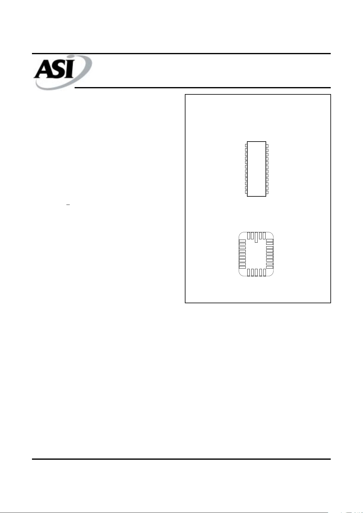
PIN ASSIGNMENT
(Top View)
AVAILABLE AS MILITARY
SPECIFICATIONS
• SMD 5962-86859
• MIL-STD-883
GENERAL DESCRIPTION
The Austin Semiconductor SRAM family employs
high-speed, low-power CMOS designs using a four-transistor
memory cell. Austin Semiconductor SRAMs are fabricated
using double-layer metal, double-layer polysilicon
technology.
For flexibility in high-speed memory applications, Austin
Semiconductor offers chip enable (CE\) and output enable
(OE\) capability. These enhancements can place the outputs
in High-Z for additional flexibility in system design.
Writing to these devices is accomplished when write
enable (WE\) and CE\ inputs are both LOW. Reading is
accomplished when WE\ remains HIGH and CE\ and OE\ go
LOW . The device offers a reduced power standby mode when
disabled. This allows system designs to achieve low standby
power requirements.
All devices operate from a single +5V power supply and
all inputs and outputs are fully TTL compatible.
16K x 4 SRAM
SRAM MEMORY ARRAY
For more products and information
please visit our web site at
www.austinsemiconductor .com
28-Pin LCC (EC)
3 2 1 28 27
13 14 15 16 17
4
5
6
7
8
9
10
11
12
26
25
24
23
22
21
20
19
18
A6
A7
A8
A9
A10
A11
A12
A13
CE\
NC
A4
A3
A2
A1
A0
DQ4
DQ3
DQ2
DQ1
WE\
NC
Vss
OE\
A5NCNC
Vcc
NC
24-Pin DIP (C)
(300 MIL)
1
2
3
4
5
6
7
8
9
10
11
12
24
23
22
21
20
19
18
17
16
15
14
13
A5
A6
A7
A8
A9
A10
A11
A12
A13
CE\
OE\
Vss
Vcc
A4
A3
A2
A1
A0
NC
DQ4
DQ3
DQ2
DQ1
WE\
SRAM
MT5C6405
Austin Semiconductor, Inc.
MT5C6405
Rev. 2.0 5/01
Austin Semiconductor, Inc. reserves the right to change products or specifications without notice.
2
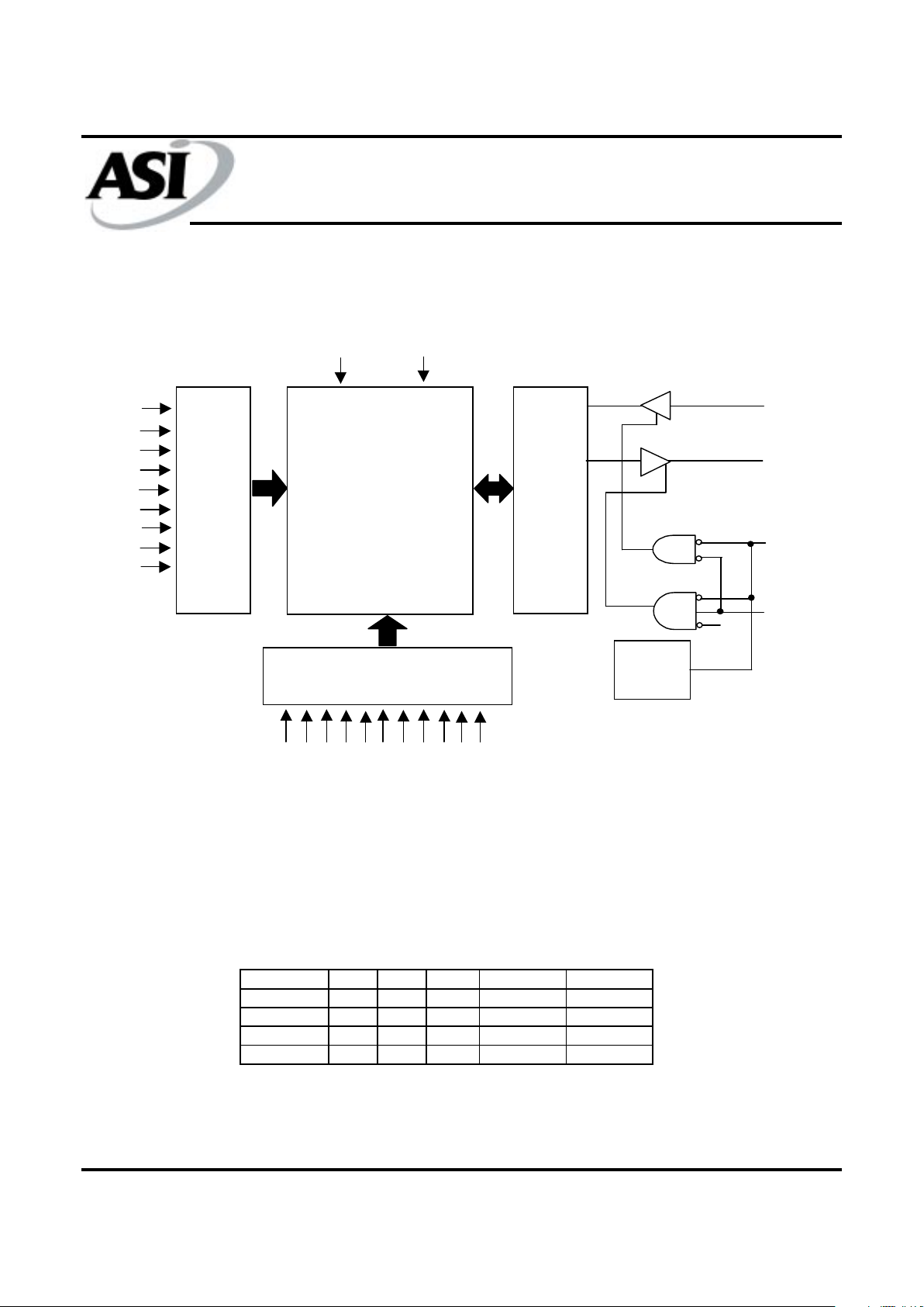
FUNCTIONAL BLOCK DIA GRAM
TRUTH TABLE
ROW DECODER
1,048,576-BIT
MEMORY ARRAY
I/O CONTROL
V
CC
GND
D
WE\
A
A
A
A
A
A
A
A
A
COLUMN DECODER
A A A A A A A A A A
POWER
DOWN
CE\
(LSB)
(LSB)
Q
OE\
MODE OE\ CE\ WE\ DQ POWER
STANDBY X H X HIGH-Z STANDBY
READ L L H Q ACTIVE
READ H L H HIGH-Z ACTIVE
WRITE X L L D ACTIVE
SRAM
MT5C6405
Austin Semiconductor, Inc.
MT5C6405
Rev. 2.0 5/01
Austin Semiconductor, Inc. reserves the right to change products or specifications without notice.
3
ABSOLUTE MAXIMUM RATINGS*
Voltage on any Input or DQ Relative to Vss....-0.5V to +7.0V
1
Storage Temperature…...................................-65oC to +150oC
Power Dissipation.................................................................1W
Max Junction T emperature..................................................+175°C
Lead T emperature (soldering 10 seconds)........................+260oC
Short Circuit Output Current...........................................20mA
*Stresses greater than those listed under "Absolute Maximum
Ratings" may cause permanent damage to the device. This is
a stress rating only and functional operation of the device at
these or any other conditions above those indicated in the
operation section of this specification is not implied. Exposure
to absolute maximum rating conditions for extended periods
may affect reliability .
ELECTRICAL CHARACTERISTICS AND RECOMMENDED DC OPERATING CONDITIONS
(-55oC < TC < 125oC; VCC = 5V +10%)
CAPACITANCE
1 All voltage referenced to Vss.
DESCRIPTION CONDITIONS SYM MIN MAX UNITS NOTES
Input High (Logic 1) Voltage
V
IH
2.2 Vcc+0.5V V 1
Input Low (Logic 0) Voltage
V
IL
-0.5 0.8 V 1, 2
Input Leakage Current
0V <
VIN < V
CC
IL
I
-10 10 µA
Output Leakage Current
Outputs Disabled
0V < V
OUT
< V
CC
IL
O
-10 10 µA
Output High Voltage
I
OH
= -4.0mA V
OH
2.4 V 1
Output Low Voltage
I
OL
= 8.0mA V
OL
0.4 V 1
SYM -12 -15 -20 -25 -35 UNITS NOTES
I
cc
140 125 110 100 90 mA 3
Power Supply
Current: Standby
I
SBT1
50 45 40 35 30 mA
I
SBC2
25 25 25 25 25 mA
Power Supply
Current: Operating
PARAMETER
CE\ >
(V
CC
-0.2); VCC = MAX
All Other Inputs <
0.2V
or >
(VCC - 0.2V), f = 0 Hz
CE\ >
VIH; VCC = MAX
f = 0 Hz
MAX
CONDITIONS
CE\ <
VIL; VCC = MAX
Output Open
DESCRIPTION CONDITIONS SYM MAX UNITS NOTES
Input Capacitance C
I
8pF 4
Output Capacitance C
O
10 pF 4
T
A
= 25oC, f = 1MHz
Vcc = 5V
SRAM
MT5C6405
Austin Semiconductor, Inc.
MT5C6405
Rev. 2.0 5/01
Austin Semiconductor, Inc. reserves the right to change products or specifications without notice.
4
ELECTRICAL CHARACTERISTICS AND RECOMMENDED AC OPERATING CONDITIONS
(Note 5) (-55oC < TC < 125oC; VCC = 5V +10%)
MIN MAX MIN MAX MIN MAX MIN MAX MIN MAX
READ CYCLE
READ cycle time
t
RC
12 15 20 25 35 ns
Address access time
t
AA
12 15 20 25 35 ns
Chip Enable access time
t
ACE
12 15 20 25 35 ns
Output hold from address change
t
OH
22222 ns
Chip Enable to output in Low-Z
t
LZCE
22222 ns7
Chip disable to output in High-Z
t
HZCE
7 8 10 12 15 ns 6, 7
Chip Enable to power-up time
t
PU
00000 ns
Chip disable to power-down time
t
PD
12 15 20 25 35 ns
Output Enable access time
t
AOE
6 7 8 10 15 ns
Output Enable to output in Low-Z
t
LZOE
00008 ns
Output disable to output in High-Z
t
HZOE
6 7 8 10 15 ns 6
WRITE CYCLE
WRITE cycle time
t
WC
12 15 20 25 35 ns
Chip Enable to end of write
t
CW
10 12 15 20 25 ns
Address valid to end of write
t
AW
10 12 15 20 25 ns
Address setup time
t
AS
00000 ns
Address hold from end of write
t
AH
00000 ns
WRITE pulse width
t
WP
10 12 15 20 25 ns
Data setup time
t
DS
7 8 10 12 15 ns
Data hold time
t
DH
00000 ns
Write disable to output in Low-Z
t
LZWE
22222 ns7
Write Enable to output in High-Z
t
HZWE
060708010015ns 6, 7
NOTES
DESCRIPTION
-12
SYMBOL UNITS
-35-25-20-15
 Loading...