

Page 1
Global LCD Panel Exchange Center
www.panelook.com
©Copyright AU Optronics, Inc.
January, 2008 All Rights Reserved. T315XW02 VT - Specs. Ver 0.5 1/31
No Reproduction and Redistribution Allowed
One step solution for LCD / PDP / OLED panel application: Datasheet, inventory and accessory!
www.panelook.com
Page 2

Global LCD Panel Exchange Center
www.panelook.com
Document Version : 0.5
Date : 2009/06/03
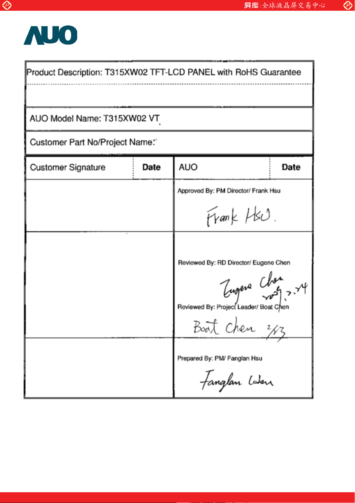
Product Specifications
31.5” WXGA Color TFT-LCD Module
Model Name: T315XW02 VT
( ) Preliminary Specifications
(*) Final Specifications
©Copyright AU Optronics, Inc.
January, 2008 All Rights Reserved. T315XW02 VT - Specs. ver 0.5 2/31
No Reproduction and Redistribution Allowed
One step solution for LCD / PDP / OLED panel application: Datasheet, inventory and accessory!
www.panelook.com
Page 3
Global LCD Panel Exchange Center
No
COVER
www.panelook.com
Contents
CONTENTS
RECORD OF REVISIONS
GENERAL DESCRIPTION 1
ABSOLUTE MAXIMUM RATINGS 2
ELECTRICAL SPECIFICATIONS 3
ELECTRICAL CHARACTREISTICS 3-1
INTERFACE CONNECTIONS 3-2
SIGNAL TIMING SPECIFICATIONS 3-3
COLOR INPUT DATA REFERNECE 3-5
SIGNAL TIMING WAVEFORMS 3-4
POWER SEQUENCE 3-6
©Copyright AU Optronics, Inc.
January, 2008 All Rights Reserved. T315XW02 VT - Specs. ver 0.5 3/31
No Reproduction and Redistribution Allowed
OPTICAL SPECIFICATIONS 4
MECHANICAL CHARACTERISTICS 5
RELIABLITY 6
INTERNATIONAL STANDARDS 7
SAFETY 7-1
EMC 7-2
PACKING 8
PRECAUTIONS 9
One step solution for LCD / PDP / OLED panel application: Datasheet, inventory and accessory!
www.panelook.com
Page 4
Global LCD Panel Exchange Center
www.panelook.com
Record of Revision
Version Date No Old Description New Description Remark
0 2008/10/31 First issue
2008/12/31 12
11 input power typ=75W
17
0.1 2009/02/04 8 4. VCIM=1.2V 4. VCIM=1.25V update
11
7 4. Measurement condition Trush=400uS 4. Measurement condition Trush=470uS update
23 Gap= 0.66 Gap= 0.66 (1.2 Max) update
0.2 2009/2/23 25 Safety: (4) EN60065: 2002; IEC 60065: 2001 add
26 Update shipping label and carton label format update
18 Brightness typ: 400nit Brightness typ: 420nit update
0.3 2009/02/27 22 Update front view drawing update
0.4 2009/3/12 21 Bezel Open vertical=398.3mm Bezel Open vertical=398.4mm update
0.5 2009/06/03 26 Add Taiwan module fab add
12
Inverter pin assignment: Pin11=Panel status d
etect. (Normal=0-0.8V. Abnormal=Open collec
tor)
Inverter pin assignment: Pin11=AUO internal
use. Keep Open.
Inverter pin assignment: Pin11=AUO internal
use. Keep Open.
Input power typ=78W
Update power sequence of inverter
Input Power (Turn on Condition)
Input Current (Turn on Condition)
Inverter pin assignment: Pin11=Panel status d
etect. (Normal=0-0.8V. Abnormal=Open collec
tor)
update
update
update
update
update
©Copyright AU Optronics, Inc.
January, 2008 All Rights Reserved. T315XW02 VT - Specs. ver 0.5 4/31
No Reproduction and Redistribution Allowed
One step solution for LCD / PDP / OLED panel application: Datasheet, inventory and accessory!
www.panelook.com
Page 5
Global LCD Panel Exchange Center
www.panelook.com
1. General Description
This specification applies to the 31.51 inch Color TFT-LCD Module T315XW02 VT. This
LCD module has a TFT active matrix type liquid crystal panel 1366x768 pixels, and
diagonal size of 31.51 inch. This module supports 1366x768 XGA-WIDE mode
(Non-interlace).
Each pixel is divided into Red, Green and Blue sub-pixels or dots which are arranged in
vertical stripes. Gray scale or the brightness of the sub-pixel color is determined with a 8-bit
gray scale signal for each dot.
The T315XW02 VT has been designed to apply the 8-bit 1 channel LVDS interface method.
It is intended to support displays where high brightness, wide viewing angle, high color
saturation, and high color depth are very important.
The T315XW02 VT model is RoHS verified which can be distinguished on panel label.
*
General Information
Items Specification Unit Note
Active Screen Size 31.51 inches
Display Area 697.685 (H) x 392.256(V) mm
Outline Dimension 760.0(H) x 450.0(V) x 45(D) mm
Driver Element a-Si TFT active matrix
Display Colors 16.7M Colors
Number of Pixels 1366 x 768 Pixel
Pixel Pitch 0.51075 mm
Pixel Arrangement RGB vertical stripe
Display Mode Normally Black
Surface Treatment Anti-Glare, 3H Haze =11%
©Copyright AU Optronics, Inc.
January, 2008 All Rights Reserved. T315XW02 VT - Specs. ver 0.5 5/31
No Reproduction and Redistribution Allowed
One step solution for LCD / PDP / OLED panel application: Datasheet, inventory and accessory!
www.panelook.com
Page 6
Global LCD Panel Exchange Center
www.panelook.com
2. Absolute Maximum Ratings
The following are maximum values which, if exceeded, may cause permanent damage to
the unit.
Item Symbol Min Max Unit Conditions
Logic/LCD Drive Voltage Vcc -0.3 14 [Volt] Note 1
Input Voltage of Signal Vin -0.3 3.6 [Volt] Note 1
BLU Input Voltage VDDB -0.3 28 [Volt] Note 1
BLU Brightness Control Voltage Vdim -0.3 7.0 [Volt] Note 1
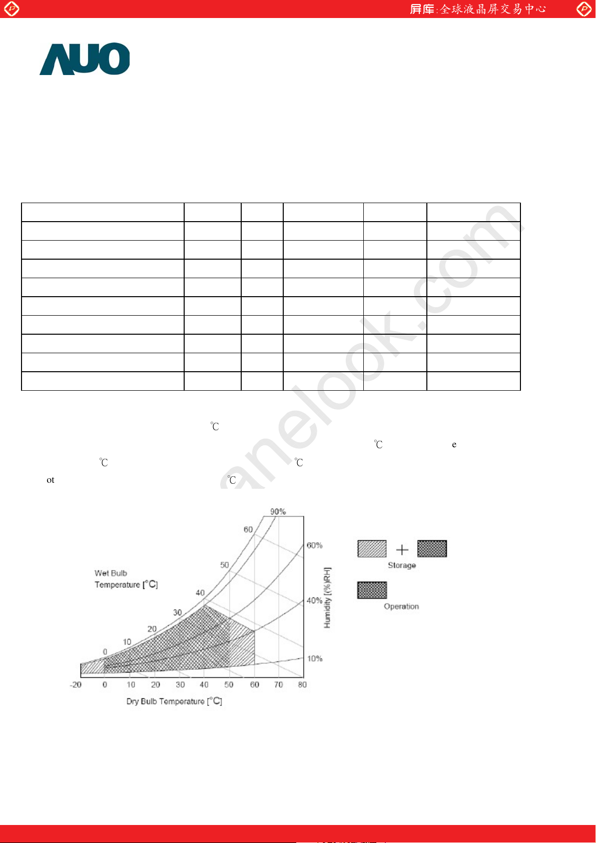
Operating Temperature TOP 0 +50 [oC] Note 2
Operating Humidity HOP 10 90 [%RH] Note 2
Storage Temperature TST -20 +60 [oC] Note 2
Storage Humidity HST 10 90 [%RH] Note 2
Panel Surface Temperature PST 65 [oC] Note 3
Note 1: Duration:50 msec.
Note 2 : Maximum Wet-Bulb should be 39 and No condensation.
The relative humidity must not exceed 90% non-condensing at temperatures of 40 or less. At tem
greater than 40 , the wet bulb temperature must not exceed 39 .
Note 3 : Surface temperature is measured at 50
кк
к
к
Dry condition
к
peratures
©Copyright AU Optronics, Inc.
January, 2008 All Rights Reserved. T315XW02 VT - Specs. ver 0.5 6/31
No Reproduction and Redistribution Allowed
One step solution for LCD / PDP / OLED panel application: Datasheet, inventory and accessory!
www.panelook.com
Page 7
Global LCD Panel Exchange Center
D
www.panelook.com
3. Electrical Specification
The T315XW02 VT requires two power inputs. One is employed to power the LCD electronics and to drive
the TFT array and liquid crystal. The second input power for the BLU, is to power inverter.
3-1 Electrical Characteristics
Parameter
Symbol
Values
Unit Notes
Min Typ Max
LCD:
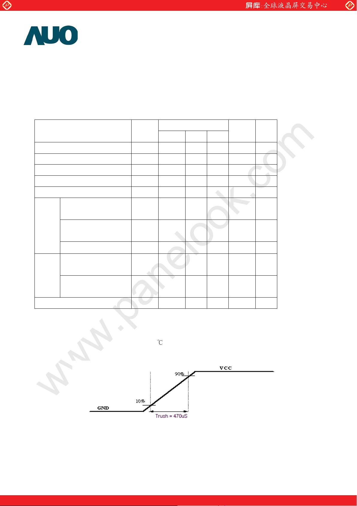
Power Supply Input Voltage Vcc 10.8 12 13.2 Vdc 1
Power Supply Input Current Icc - 0.45 0.55 A 2
Power Consumption Pc - 5.4
Inrush Current I
LV DS
Interface
CMOS
ifferential Input High Threshold
Vo l t a g e
Differential Input Low Threshold
Vo l t a g e
Common Input Voltage
Input High Threshold Voltage
Interface
Input Low Threshold Voltage
- - 6 Apeak 3
RUSH
VTH - - 100 mV 4
VTL -100 - - mV 4
VCIM 1.10 1.25 1.40 V 4
VIH
2.4 3.3 Vdc
(High)
VIL
0 0.7 Vdc
7.26 Watt 2
(Low)
Life Time 50,000 Hours 5,6,7,8
Note :
1. The ripple voltage should be controlled under 10% of V
=
f
2. Vcc=12.0V,
60Hz, fCLK=81.5Mhz , 25 , Test Pattern : White Patternк
v
CC
3. Measurement condition :
©Copyright AU Optronics, Inc.
January, 2008 All Rights Reserved. T315XW02 VT - Specs. ver 0.5 7/31
No Reproduction and Redistribution Allowed
One step solution for LCD / PDP / OLED panel application: Datasheet, inventory and accessory!
www.panelook.com
Page 8
Global LCD Panel Exchange Center
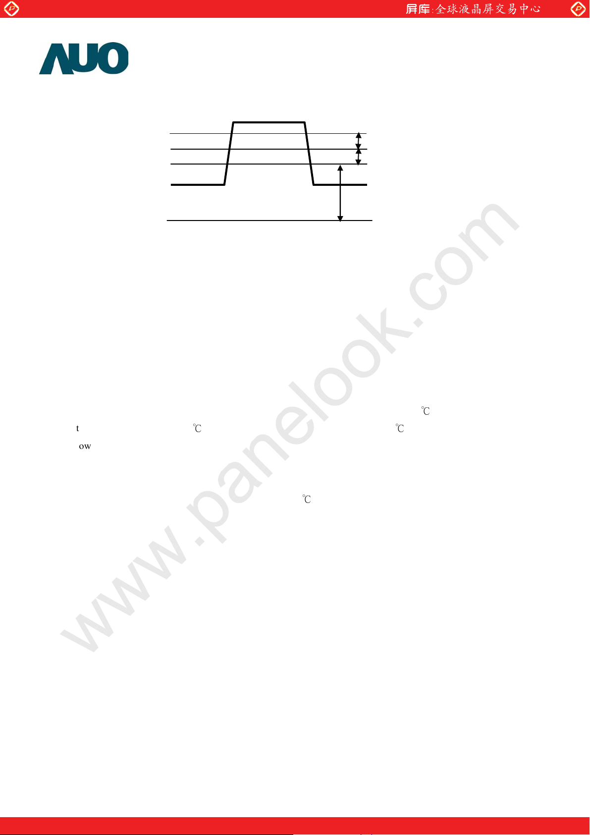
4. VCIM = 1.25V
www.panelook.com
VCIM
VTH
VIL
0V
5. The performance of the Lamp in LCD panel, for example life time or brightness, is extremely
influenced by the characteristics of the DC-AC Inverter. So all the parameters of an inverter should
be carefully designed as not to produce too much leakage current from high-voltage output of the
inverter. When you design or order the inverter, please make sure unwanted lighting caused by the
mismatch of the lamp and the inverter (no lighting, flicker, etc) never occurs. After confirmation, the
LCD panel should be operated in the same condition as installed in your instrument.
6. Do not attach a conducting tape to lamp connecting wire. If the lamp wire attach to conducting tape,
TFT-LCD Module have a low luminance and the inverter has abnormal action because leakage
current occurs between lamp wire and conducting tape.
7. The relative humidity must not exceed 80% non-condensing at temperatures of 40 or less. At
temperatures greater than 40 , the wet bulb temperature must not exceed 39 . When operate at
кк
к
low temperatures, the brightness of CCFL will drop and the life time of CCFL will be reduced.
8. Specified values are for a single lamp only which is aligned horizontally. The lifetime is defined as
the time which luminance of the lamp is 50% compared to its original value.
к
[Operating condition: Continuous operating at Ta = 25±2
]
©Copyright AU Optronics, Inc.
January, 2008 All Rights Reserved. T315XW02 VT - Specs. ver 0.5 8/31
No Reproduction and Redistribution Allowed
One step solution for LCD / PDP / OLED panel application: Datasheet, inventory and accessory!
www.panelook.com
Page 9
Global LCD Panel Exchange Center
www.panelook.com
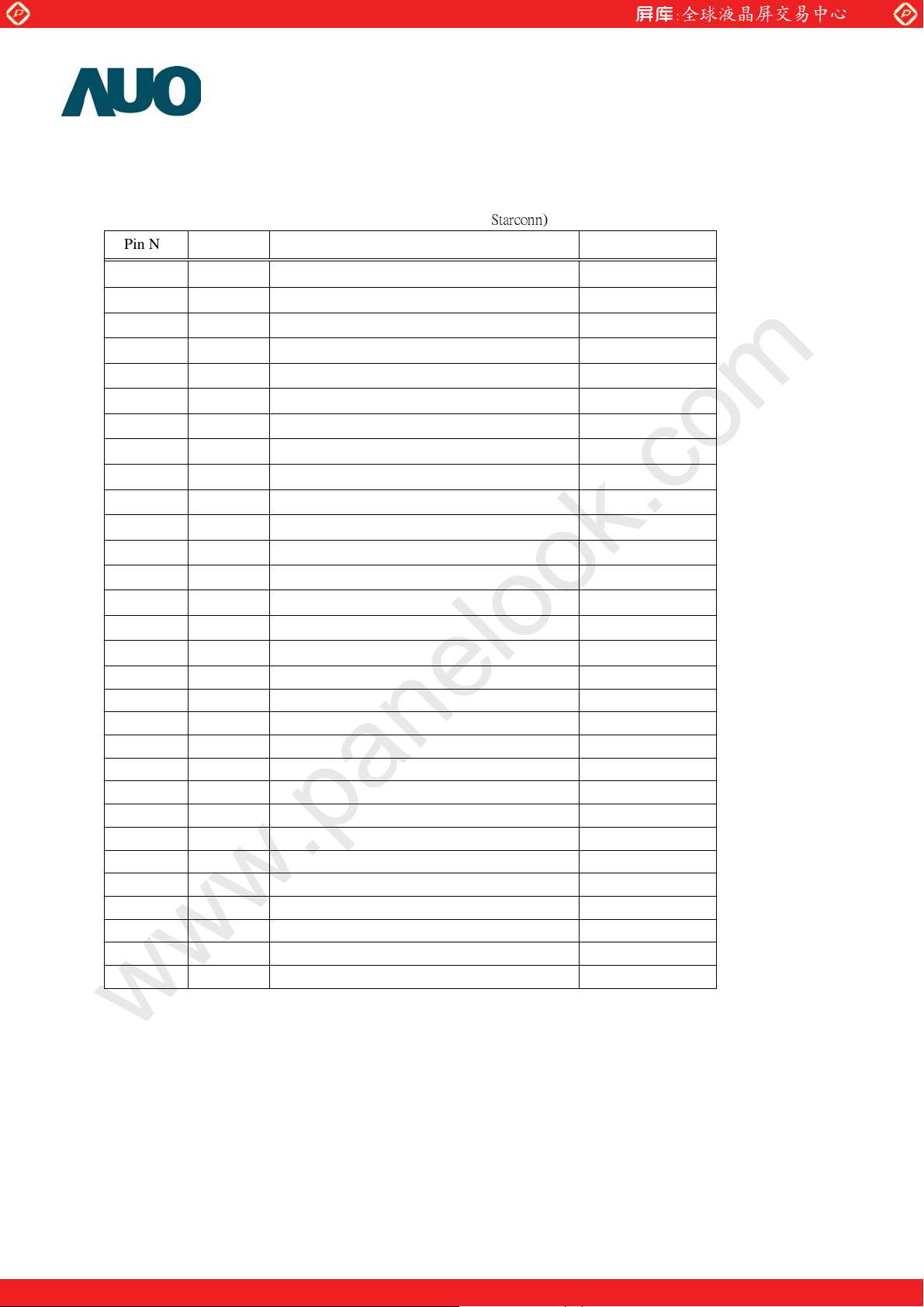
3-2 Interface Connections
-
Connector on Panel: 093G30-B0001A-1 (Manufactured by
Pin No Symbol Description Default
1 VCC +12V, DC, Regulated
2 VCC +12V, DC, Regulated
3 VCC +12V, DC, Regulated
4 VCC +12V, DC, Regulated
5 GND Ground and Signal Return
6 GND Ground and Signal Return
7 GND Ground and Signal Return
8 GND Ground and Signal Return
9 LVDS Option Low/Open for Normal (NS), High for JEIDA NS mode
10 Reserved Open AUO internal test
11 GND Ground and Signal Return for LVDS
12 RIN0- LVDS Channel 0 negative
13 RIN0+ LVDS Channel 0 positive
14 GND Ground and Signal Return for LVDS
15 RIN1- LVDS Channel 1 negative
16 RIN1+ LVDS Channel 1 positive
17 GND Ground and Signal Return for LVDS
18 RIN2- LVDS Channel 2 negative
19 RIN2+ LVDS Channel 2 positive
20 GND Ground and Signal Return for LVDS
21 RCLK- LVDS Clock negative
22 RCLK+ LVDS Clock positive
23 GND Ground and Signal Return for LVDS
24 RIN3- LVDS Channel 3 negative
25 RIN3+ LVDS Channel 3 positive
26 GND Ground and Signal Return for LVDS
27 Reserved Open or High AUO internal test
28 Reserved Open or High AUO internal test
29 GND Ground and Signal Return
30 GND Ground and Signal Return
Note:
1. All GND (ground) pins should be connected together and should also be connected to the LCD’s
metal frame. All Vcc (power input) pins should be connected together.
2. For Pin 10, 27 and 28, panel will not damage if negligently connect these pins to high or low
©Copyright AU Optronics, Inc.
January, 2008 All Rights Reserved. T315XW02 VT - Specs. ver 0.5 9/31
No Reproduction and Redistribution Allowed
ʳ˦˴˶
)
One step solution for LCD / PDP / OLED panel application: Datasheet, inventory and accessory!
www.panelook.com
Page 10
Global LCD Panel Exchange Center
LVDS Option = High (JEIDA)
www.panelook.com
LVDS Option = Low or Open (NS)
©Copyright AU Optronics, Inc.
January, 2008 All Rights Reserved. T315XW02 VT - Specs. ver 0.5 10/31
No Reproduction and Redistribution Allowed
One step solution for LCD / PDP / OLED panel application: Datasheet, inventory and accessory!
www.panelook.com
Page 11

Global LCD Panel Exchange Center
www.panelook.com
BACKLIGHT CONNECTOR PIN CONFIGURATION
1. Electrical specification
Note 1 : Measurement condition Rising time = 20 ms (VDDB : 10%~90%);
ΰ
Ta=25±5 , Turn on for 45minutes
Note 2 : VDIM= 3.3V (MAX, 100% brightness), VDIM= 0V (MIN, 10% brightness)
Note 3 : (a) Uniformity and flicker does not guarantee under 20% dimming control.
(b) 10% dimming function okay and no backlight shut down
к
©Copyright AU Optronics, Inc.
January, 2008 All Rights Reserved. T315XW02 VT - Specs. Ver 0.5 11/31
No Reproduction and Redistribution Allowed
α
One step solution for LCD / PDP / OLED panel application: Datasheet, inventory and accessory!
www.panelook.com
Page 12

Global LCD Panel Exchange Center
2. Input specification
CN1: CI0114M1HRL-LF (Manufactured by Civilux)
www.panelook.com
©Copyright AU Optronics, Inc.
January, 2008 All Rights Reserved. T315XW02 VT - Specs. ver 0.5 12/31
No Reproduction and Redistribution Allowed
One step solution for LCD / PDP / OLED panel application: Datasheet, inventory and accessory!
www.panelook.com
Page 13

Global LCD Panel Exchange Center
www.panelook.com
3-3 Signal Timing Specifications
This is the signal timing required at the input of the User connector. All of the interface signal timing should be
satisfied with the following specifications for it’s proper operation.
* Timing Table
DE only Mode
Vertical Frequency:
Notes:
1.) Display position is specific by the rise of DE signal only.
Horizontal display position is specified by the rising edge of 1
edge of the screen.
Vertical display position is specified by the rise of DE after a “Low” level period equivalent to eight times of horizontal
period. The 1
2.) The display position does not fit to the screen if a period of DE “High” and the effective data period do not
synchronize with each other.
st
data corresponding to one horizontal line after the rise the of 1st DE is displayed at the top line of screen.
st
DCLK after the rise of 1st DE, is displayed on the left
©Copyright AU Optronics, Inc.
January, 2008 All Rights Reserved. T315XW02 VT - Specs. ver 0.5 13/31
No Reproduction and Redistribution Allowed
One step solution for LCD / PDP / OLED panel application: Datasheet, inventory and accessory!
www.panelook.com
Page 14

Global LCD Panel Exchange Center
3-4 Signal Timing Waveforms
1366
RGB Data
DE
Pix el
Invalid Data
Tcl k
www.panelook.com
CLK
RGB
Dat a
Line
768
Invalid Data Invalid Data
DE
Line
Pixel
1
Pix el
2
Pix el
3
Pix el
4
Pix el
5
Pix el
6
1366
Pix el
Invalid Data
Tdisp(h)
Th
1
Line
2
Line
3
Line
4
Line
768
Th
Tv
Tdis p(v)
Pix el
1
Pix el
2
©Copyright AU Optronics, Inc.
January, 2008 All Rights Reserved. T315XW02 VT - Specs. Ver 0.5 14/31
No Reproduction and Redistribution Allowed
One step solution for LCD / PDP / OLED panel application: Datasheet, inventory and accessory!
www.panelook.com
Page 15

Global LCD Panel Exchange Center
www.panelook.com
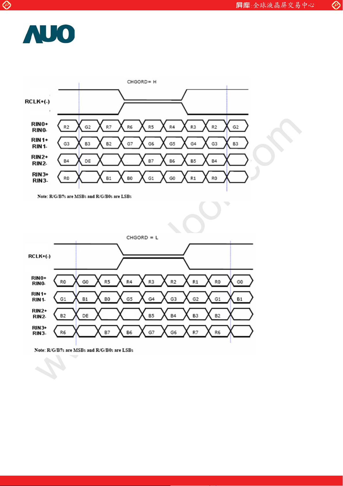
3-5 Color Input Data Reference
The brightness of each primary color (red, green and blue) is based on the 8 bit gray scale data input for the
color; the higher the binary input, the brighter the color. The table below provides a reference for color versus
data input.
COLOR DATA REFERENCE
Color
Basic
Color
RED
Input Color Data
RED
MSB LSB
R7 R6 R5 R4 R3 R2 R1 R0 G7 G6 G5 G4 G3 G2 G1 G0 B7 B6 B5 B4 B3 B2 B1 B0
Black 0 0 0 0 0 0 0 0 0 0 0 0 0 0 0 0 0 0 0 0 0 0 0 0
Red(255) 1 1 1 1 1 1 1 1 0 0 0 0 0 0 0 0 0 0 0 0 0 0 0 0
Green(255) 0 0 0 0 0 0 0 0 1 1 1 1 1 1 1 1 0 0 0 0 0 0 0 0
Blue(255) 0 0 0 0 0 0 0 0 0 0 0 0 0 0 0 0 1 1 1 1 1 1 1 1
Cyan 0 0 0 0 0 0 0 0 1 1 1 1 1 1 1 1 1 1 1 1 1 1 1 1
Magenta 1 1 1 1 1 1 1 1 0 0 0 0 0 0 0 0 1 1 1 1 1 1 1 1
Yellow 1 1 1 1 1 1 1 1 1 1 1 1 1 1 1 1 0 0 0 0 0 0 0 0
White 1 1 1 1 1 1 1 1 1 1 1 1 1 1 1 1 1 1 1 1 1 1 1 1
RED(000) 0 0 0 0 0 0 0 0 0 0 0 0 0 0 0 0 0 0 0 0 0 0 0 0
RED(001) 0 0 0 0 0 0 0 1 0 0 0 0 0 0 0 0 0 0 0 0 0 0 0 0
----
RED(254) 1 1 1 1 1 1 1 0 0 0 0 0 0 0 0 0 0 0 0 0 0 0 0 0
MSB LSB
GREEN
BLUE
MSB LSB
RED(255) 1 1 1 1 1 1 1 1 0 0 0 0 0 0 0 0 0 0 0 0 0 0 0 0
GREEN
BLUE
©Copyright AU Optronics, Inc.
January, 2008 All Rights Reserved. T315XW02 VT - Specs. Ver 0.5 15/31
No Reproduction and Redistribution Allowed
GREEN(000) 0 0 0 0 0 0 0 0 0 0 0 0 0 0 0 0 0 0 0 0 0 0 0 0
GREEN(001) 0 0 0 0 0 0 0 0 0 0 0 0 0 0 0 1 0 0 0 0 0 0 0 0
----
GREEN(254) 0 0 0 0 0 0 0 0 1 1 1 1 1 1 1 0 0 0 0 0 0 0 0 0
GREEN(255) 0 0 0 0 0 0 0 0 1 1 1 1 1 1 1 1 0 0 0 0 0 0 0 0
BLUE(000) 0 0 0 0 0 0 0 0 0 0 0 0 0 0 0 0 0 0 0 0 0 0 0 0
BLUE(001) 0 0 0 0 0 0 0 0 0 0 0 0 0 0 0 0 0 0 0 0 0 0 0 1
-------
BLUE(254) 0 0 0 0 0 0 0 0 0 0 0 0 0 0 0 0 1 1 1 1 1 1 1 0
BLUE(255) 0 0 0 0 0 0 0 0 0 0 0 0 0 0 0 0 1 1 1 1 1 1 1 1
One step solution for LCD / PDP / OLED panel application: Datasheet, inventory and accessory!
www.panelook.com
Page 16

Global LCD Panel Exchange Center
3-6 Power Sequence for LCD Module
3.6.1 Power Sequence for LCD
www.panelook.com
Va lu es Parameter
Min. Typ. Max.
t1 0.4 - 30 ms
t2 0.1 - 50 ms
t3 200 - - ms
t4 10 - - ms
t5 0.1 - 50 ms
t6 - 300 ms
t7 500 - - ms
Units
Note:
The timing controller will not be damaged in case of TV set AC input power suddenly shut down.
Once power reset, it should follow power sequence as spec. definition.
(1) Apply the lamp voltage within the LCD operation range. When the back-light turns on before the LCD
operation or the LCD turns off before the back-light turns off, the display may momentarily become
abnormal screen.
©Copyright AU Optronics, Inc.
January, 2008 All Rights Reserved. T315XW02 VT - Specs. Ver 0.5 16/31
No Reproduction and Redistribution Allowed
One step solution for LCD / PDP / OLED panel application: Datasheet, inventory and accessory!
www.panelook.com
Page 17

Global LCD Panel Exchange Center
3.6.2 Power Sequence for Inverter
www.panelook.com
Va lu es Parameter
Min. Typ. Max.
T1 20 - - Ms
T2 50 - - Ms
T3 0 - - Ms
T4 0 - - Ms
T5 0 - - Ms
T6 - - 10 Ms
Units
©Copyright AU Optronics, Inc.
January, 2008 All Rights Reserved. T315XW02 VT - Specs. ver 0.5 17/31
No Reproduction and Redistribution Allowed
One step solution for LCD / PDP / OLED panel application: Datasheet, inventory and accessory!
www.panelook.com
Page 18

Global LCD Panel Exchange Center
www.panelook.com
4. Optical Specification
Optical characteristics are determined after the unit has been ‘ON’ and stable for approximately 45 minutes in
a dark environment at 25 . The values specified are at an approximate distance 50cm from the LCD surface
at a viewing angle of ĭ and șequal to 0°.
Fig.1 1 presents additional information concerning the measurement equipment and method.
Parameter
Contrast Ratio CR 2400 3000 1
Surface Luminance, white LWH 350 420
к
Symbol
SR3 or equivalent
Val ue s
Min. Typ. Max.
Units Notes
cd/
ф
2
Luminance Variation į
G to G Response time
9 p 1.30 3
WHITE
TȖ
6.5 ms 4
Color Gamut NTSC 72 %
Color Coordinates
RED RX 0.64
R
0.33
Y
GREEN GX 0.28
G
0.60
Y
Typ.-0 .03
Typ.+0.03
BLUE BX 0.15
B
0.05
Y
WHITE WX 0.28
W
Y
0.29
Viewing Angle
x axis, right(ij=0°) șr 89 Degree 5
x axis, left(ij=180°) șl 89 Degree 5
y axis, up(ij=90°) șu 89 Degree 5
y axis, down (ij=0°) ș
89 Degree 5
d
©Copyright AU Optronics, Inc.
January, 2008 All Rights Reserved. T315XW02 VT - Specs. ver 0.5 18/31
No Reproduction and Redistribution Allowed
One step solution for LCD / PDP / OLED panel application: Datasheet, inventory and accessory!
www.panelook.com
Page 19

Global LCD Panel Exchange Center
Note:
1. Contrast Ratio (CR) is defined mathematically as:
Surface Luminance of
Contrast Ratio=
2. Surface luminance is luminance value at point 5 across the LCD surface 50cm from the surface with all
Surface Luminance of
www.panelook.com
L
on5
L
off5
pixels displaying white. For more information see FIG 2. When VDDB = 24V, IDDB = 5A, L
where Lon5 is the luminance with all pixels displaying white at center 5 location.
3. The variation in surface luminance, įWHITE is defined (center of Screen) as:
į
WHITE(9P)
4. Response time TȖ is the average time required for display transition by switching the input signal for five
luminance ratio (0%,25%,50%,75%,100% brightness matrix) and is based on f
= Maximum(L
on1
, L
on2
,…,L
)/ Minimum(L
on9
on1
, L
,…L
on2
v
on9
=60Hz to optimize.
)
=Lon5,
WH
FIG. 2 Luminance
©Copyright AU Optronics, Inc.
January, 2008 All Rights Reserved. T315XW02 VT - Specs. Ver 0.5 19/31
No Reproduction and Redistribution Allowed
One step solution for LCD / PDP / OLED panel application: Datasheet, inventory and accessory!
www.panelook.com
Page 20

Global LCD Panel Exchange Center
5. Viewing angle is the angle at which the contrast ratio is greater than 10. The angles are determined for the
horizontal or x axis and the vertical or y axis with respect to the z axis which is normal to the LCD surface.
For more information see FIG4.
www.panelook.com
FIG. 3 Response Time
The response time is defined as the following figure and shall be measured by switching the input signal for
“any level of gray(bright) “ and “any level of gray(dark)”.
Any level of gray(Bright) Any level of gray(Dark) Any level of gray(Bright)
FIG. 4 Viewing angle
©Copyright AU Optronics, Inc.
January, 2008 All Rights Reserved. T315XW02 VT - Specs. ver 0.5 20/31
No Reproduction and Redistribution Allowed
One step solution for LCD / PDP / OLED panel application: Datasheet, inventory and accessory!
www.panelook.com
Page 21

Global LCD Panel Exchange Center
www.panelook.com
5. Mechanical Characteristics
The contents provide general mechanical characteristics for the model T315XW02 VT. In addition the figures
in the next page are detailed mechanical drawing of the LCD.
Outline Dimension
Weight 6000g Typ.
Surface Treatment AG, 3H
Horizontal 760.0mm
Vertical 450.0mm
Depth 45mm
Horizontal 703.6mm Bezel Opening
Vertical 398.4mm
Horizontal 697.685mm Active Display Area
Vertical 392.256mm
©Copyright AU Optronics, Inc.
January, 2008 All Rights Reserved. T315XW02 VT - Specs. ver 0.5 21/31
No Reproduction and Redistribution Allowed
One step solution for LCD / PDP / OLED panel application: Datasheet, inventory and accessory!
www.panelook.com
Page 22

Global LCD Panel Exchange Center
Front:
www.panelook.com
©Copyright AU Optronics, Inc.
January, 2008 All Rights Reserved. T315XW02 VT - Specs. Ver 0.5 22/31
No Reproduction and Redistribution Allowed
One step solution for LCD / PDP / OLED panel application: Datasheet, inventory and accessory!
www.panelook.com
Page 23

Global LCD Panel Exchange Center
Back:
www.panelook.com
©Copyright AU Optronics, Inc.
January, 2008 All Rights Reserved. T315XW02 VT - Specs. ver 0.5 23/31
No Reproduction and Redistribution Allowed
One step solution for LCD / PDP / OLED panel application: Datasheet, inventory and accessory!
www.panelook.com
Page 24

Global LCD Panel Exchange Center
6. Reliability:
Environment test condition
No Test Item Condition
1 High temperature storage test
2 Low temperature storage test
3 High temperature operation test
4 Low temperature operation test
5 Vibration test
(non-operating)
6 Shock test
(non-operating)
7 Vibration test
www.panelook.com
Ta= 60
к
300h
Ta= -20
к
300h
Ta= 50
к
300h
Ta= -5
к
300h
"(10 ~ 300Hz/1.5G/11min SR, XYZ 30min/axis)
Vibration level : 1.5G RMS, Bandwidth : 10-300Hz
Duration: X, Y, Z 30min, "
Shock level: 50G
Waveform: half since wave, 11ms
Direction: X, Y, Z, one time each direction
Random wave (1.5 Grms 10~200Hz)
(with carton)
8 Drop test
(with carton)
30mins / Per each X.Y.Z axes "
Height: 38cm
1 corner, 3 edges, 6 surfaces
(ASTMD4169-I)
©Copyright AU Optronics, Inc.
January, 2008 All Rights Reserved. T315XW02 VT - Specs. ver 0.5 24/31
No Reproduction and Redistribution Allowed
One step solution for LCD / PDP / OLED panel application: Datasheet, inventory and accessory!
www.panelook.com
Page 25

Global LCD Panel Exchange Center
7. International Standard
7-1. Safety
(1) UL1950 Third Edition, Underwriters Laboratories, Inc. Jan. 28, 1995
Standard for Safety of Information Technology Equipment Including electrical Business Equipment.
(2) CAN/CSA C22.2 No. 950-95/60950 Third Edition, Canadian Standards Association,
Standard for Safety of Information Technology Equipment Including Electrical Business Equipment.
(3) EN60950 : 1992+A2: 1993+A2: 1993+C3: 1995+A4: 1997+A11: 1997
IEC 950: 1991+A1: 1992+A2: 1993+C3: 1995+A4:1996
European Committee for Electrotechnical Standardization (CENELEC)
EUROPEAN STANDARD for Safety of Information Technology Equipment Including Electrical
Business Equipment.
www.panelook.com
(4) EN60065: 2002; IEC 60065: 2001
7-2. EMC
a) ANSI C63.4 “Methods of Measurement of Radio-Noise Emissions from Low-Voltage Electrical and
Electrical Equipment in the Range of 9kHz to 40GHz. “American National standards
Institute(ANSI), 1992
b) C.I.S.P.R “Limits and Methods of Measurement of Radio Interface Characteristics of Information
Technology Equipment.” International Special committee on Radio Interference.
c) EN 55022 “Limits and Methods of Measurement of Radio Interface Characteristics of Information
Technology Equipment.” European Committee for Electrotechnical Standardization. (CENELEC),
1998
©Copyright AU Optronics, Inc.
January, 2008 All Rights Reserved. T315XW02 VT - Specs. Ver 0.5 25/31
No Reproduction and Redistribution Allowed
One step solution for LCD / PDP / OLED panel application: Datasheet, inventory and accessory!
www.panelook.com
Page 26

Global LCD Panel Exchange Center
–
–
8. Packing
Panel label:
www.panelook.com
*838A0584AHZZ
AU Optronics XXXXG Made in China (S1)
Manufactured 09/02 AM89018 Model NO: T315XW02 VT
*838A0584AHZZ
AU Optronics XXXXG Made in Taiwan (MA)
Manufactured 09/02 AM89018 Model NO: T315XW02 VT
838A0584AHZ
– ZS0200
ZS0200*
ZM1100*
838A0584AHZZ: Panel Unique ID
ZS0200: AUO internal use
Manufactured 09/02
2009 week 02
AM89018
AUO internal use
Carton Label:
©Copyright AU Optronics, Inc.
January, 2008 All Rights Reserved. T315XW02 VT - Specs. Ver 0.5 26/31
No Reproduction and Redistribution Allowed
One step solution for LCD / PDP / OLED panel application: Datasheet, inventory and accessory!
www.panelook.com
Page 27

Global LCD Panel Exchange Center
Carton:
www.panelook.com
©Copyright AU Optronics, Inc.
January, 2008 All Rights Reserved. T315XW02 VT - Specs. ver 0.5 27/31
No Reproduction and Redistribution Allowed
One step solution for LCD / PDP / OLED panel application: Datasheet, inventory and accessory!
www.panelook.com
Page 28

Global LCD Panel Exchange Center
www.panelook.com
Item
Qty. Dimension Weight (kg)
1 Packing BOX 4pcs/box 832(L)mm*283(W)mm*545(H)mm 30.5
2 Pallet 1 1150(L)mm*840(W)mm*138(H)mm 13
3 Boxes per Pallet 8 boxes/Pallet
4 Panels per Pallet 32pcs/pallet
Pallet after packing 32 1150(L)mm*840(W)mm*2460(H)mm 256
Specification
Packing Remark
©Copyright AU Optronics, Inc.
January, 2008 All Rights Reserved. T315XW02 VT - Specs. ver 0.5 28/31
No Reproduction and Redistribution Allowed
One step solution for LCD / PDP / OLED panel application: Datasheet, inventory and accessory!
www.panelook.com
Page 29

Global LCD Panel Exchange Center
9. PRECAUTIONS
Please pay attention to the followings when you use this TFT LCD module.
9-1 MOUNTING PRECAUTIONS
(1) You must mount a module using holes arranged in four corners or four sides.
(2) You should consider the mounting structure so that uneven force (ex. Twisted stress) is not
applied to module. And the case on which a module is mounted should have sufficient strength so
that external force is not transmitted directly to the module.
(3) Please attach the surface transparent protective plate to the surface in order to protect the
polarizer. Transparent protective plate should have sufficient strength in order to the resist external
force.
(4) You should adopt radiation structure to satisfy the temperature specification.
(5) Acetic acid type and chlorine type materials for the cover case are not desirable because the
former generates corrosive gas of attacking the polarizer at high temperature and the latter
causes circuit break by electro-chemical reaction.
(6) Do not touch, push or rub the exposed polarizer with glass, tweezers or anything harder than
HB pencil lead. And please do not rub with dust clothes with chemical treatment. Do not
touch the surface of polarizer for bare hand or greasy cloth. (Some cosmetics are detrimental
to the polarizer.)
(7) When the surface becomes dusty, please wipe gently with absorbent cotton or other soft
materials like chamois soaks with petroleum benzene. Normal-hexane is recommended for
cleaning the adhesives used to attach front/ rear polarizer. Do not use acetone, toluene and
alcohol because they cause chemical damage to the polarizer.
(8) Wipe off saliva or water drops as soon as possible. Their long time contact with polarizer
causes deformations and color fading.
(9) Do not open the case because inside circuits do not have sufficient strength.
www.panelook.com
9-2 OPERATING PRECAUTIONS
(1) The device listed in the product specification sheets was designed and manufactured for TV
application
(2) The spike noise causes the mis-operation of circuits. It should be lower than following voltage:
V=±200mV(Over and under shoot voltage)
(3) Response time depends on the temperature. (In lower temperature, it becomes longer..)
(4) Brightness depends on the temperature. (In lower temperature, it becomes lower.) And in
lower temperature, response time (required time that brightness is stable after turned on)
becomes longer.
(5) Be careful for condensation at sudden temperature change. Condensation makes damage to
polarizer or electrical contacted parts. And after fading condensation, smear or spot will occur.
(6) When fixed patterns are displayed for a long time, remnant image is likely to occur.
(7) Module has high frequency circuits. Sufficient suppression to the electromagnetic interference
shall be done by system manufacturers. Grounding and shielding methods may be important
to minimize the interface.
©Copyright AU Optronics, Inc.
January, 2008 All Rights Reserved. T315XW02 VT - Specs. ver 0.5 29/31
No Reproduction and Redistribution Allowed
One step solution for LCD / PDP / OLED panel application: Datasheet, inventory and accessory!
www.panelook.com
Page 30

Global LCD Panel Exchange Center
www.panelook.com
9-3 ELECTROSTATIC DISCHARGE CONTROL
Since a module is composed of electronic circuits, it is not strong to electrostatic discharge. Make certain that
treatment persons are connected to ground through wrist band etc. And don’t touch interface pin directly.
9-4 PRECAUTIONS FOR STRONG LIGHT EXPOSURE
Strong light exposure causes degradation of polarizer and color filter.
9-5 STORAGEЀЀЀЀ
When storing modules as spares for a long time, the following precautions are necessary.
(1) Store them in a dark place. Do not expose the module to sunlight or fluorescent light. Keep the
temperature between 5 and 35 at normal humidity.
(2) The polarizer surface should not come in contact with any other object. It is recommended that they be
stored in the container in which they were shipped.
кк
9-6 HANDLING PRECAUTIONS FOR PROTECTION FILM
(1) The protection film is attached to the bezel with a small masking tape. When the protection film is peeled
off, static electricity is generated between the film and polarizer. This should be peeled off slowly and
carefully by people who are electrically grounded and with well ion-blown equipment or in such a
condition, etc.
(2) When the module with protection film attached is stored for a long time, sometimes there remains a very
small amount of flue still on the Bezel after the protection film is peeled off.
(3) You can remove the glue easily. When the glue remains on the Bezel or its vestige is recognized, please
wipe them off with absorbent cotton waste or other soft material like chamois soaked with normal-hexane.
©Copyright AU Optronics, Inc.
January, 2008 All Rights Reserved. T315XW02 VT - Specs. ver 0.5 30/31
No Reproduction and Redistribution Allowed
One step solution for LCD / PDP / OLED panel application: Datasheet, inventory and accessory!
www.panelook.com
Page 31

Global LCD Panel Exchange Center
Appendix A
1. EMI specification
Item Min Typ Max Unit
EMI level (Note) --- --- -6 dB(ȝV/m)
SSCG --- 300 --- ps
Model name: T315XW02 VT
Note:
(a). Criteria: CISPR22
(b). Signal generator: PSG400 (Sony EMCS)
(c). EMI site: Sony EMCS Ichinomiya Tec. or using correlation value
(d). Find result should be checked by connecting with TV-set
www.panelook.com
©Copyright AU Optronics, Inc.
January, 2008 All Rights Reserved. T315XW02 VT - Specs. ver 0.5 31/31
No Reproduction and Redistribution Allowed
One step solution for LCD / PDP / OLED panel application: Datasheet, inventory and accessory!
www.panelook.com
 Loading...