

AUO T315XW01 V5 Specification

Product Specifications
31.5” WXGA Color TFT-LCD Module
Model Name: T315XW01 V5
(*) Preliminary Specifications
( ) Final Specifications
©Copyright AU Optronics, Inc.
January, 2003 All Rights Reserved. T315XW01 V5 - Specs. Ver 0.1 1/25
No Reproduction and Redistribution Allowed
No
Contents
COVER
RECORD OF REVISIONS
CONTENTS
GENERAL DESCRIPTION 1
ABSOLUTE MAXIMUM RATINGS 2
ELECTRICAL SPECIFICATIONS 3
ELECTRICAL CHARACTREISTICS 3-1
INTERFACE CONNECTIONS 3-2
SIGNAL TIMING SPECIFICATIONS 3-3
COLOR INPUT DATA REFERNECE 3-5
SIGNAL TIMING WAVEFORMS 3-4
POWER SEQUENCE 3-6
OPTICAL SFECIFICATIONS 4
MECHANICAL CHARACTERISTICS 5
RELIABLITY 6
INTERNATIONAL STANDARDS 7
SAFETY 7-1
EMC 7-2
Packing 8
PRECAUTIONS 9
©Copyright AU Optronics, Inc.
January, 2003 All Rights Reserved. T315XW01 V5 - Specs. Ver 0.1 2/25
No Reproduction and Redistribution Allowed
Record of Revision
Version
0.1 2005/5/20 All All First Issued
Date No Old Description New Description Remark
0.2 2005/6/13
9 VDIM : 0 ~ 5V VDIM : 0 ~ 3.3V Update
©Copyright AU Optronics, Inc.
January, 2003 All Rights Reserved. T315XW01 V5 - Specs. Ver 0.1 3/25
No Reproduction and Redistribution Allowed
1. General Description
This specification applies to the 31.51 inch Color TFT-LCD Module T315XW01 V5. This
LCD module has a TFT active matrix type liquid crystal panel 1366x768 pixels, and diagonal
size of 31.51 inch. This module supports 1366x768 XGA-WIDE mode (Non-interlace).
Each pixel is divided into Red, Green and Blue sub-pixels or dots which are arranged in
vertical stripes. Gray scale or the brightness of the sub-pixel color is determined with a 8-bit
gray scale signal for each dot.
The T315XW01 V5 has been designed to apply the 8-bit 1 channel LVDS interface method.
It is intended to support displays where high brightness, wide viewing angle, high color
saturation, and high color depth are very important.
* General Information
Items Specification Unit Note
Active Screen Size 31.51 inches
Display Area 697.68 (H) x 392.26(V) mm
Outline Dimension 760.0(H) x 450.0(V) x 45(D) mm With inverter
Driver Element a-Si TFT active matrix
Display Colors 16.7M Colors
Number of Pixels 1366 x 768 Pixel
Pixel Pitch 0.51075 mm
Pixel Arrangement RGB vertical stripe
Display Mode Normally Black
Surface Treatment AG, 3H
©Copyright AU Optronics, Inc.
January, 2003 All Rights Reserved. T315XW01 V5 - Specs. Ver 0.1 4/25
No Reproduction and Redistribution Allowed
2. Absolute Maximum Ratings
The following are maximum values which, if exceeded, may cause permanent damage to the
unit.
Item Symbol Min Max Unit Conditions
Logic/LCD Drive Voltage VDD -0.3 5.5 [Volt] Note 1
Input Voltage of Signal Vin -0.3 3.6 [Volt] Note 1
BLU Input Voltage VDDB -0.3 27 [Volt] Note 1
BLU Brightness Control Voltage BLON -0.3 7.0 [Volt] Note 1
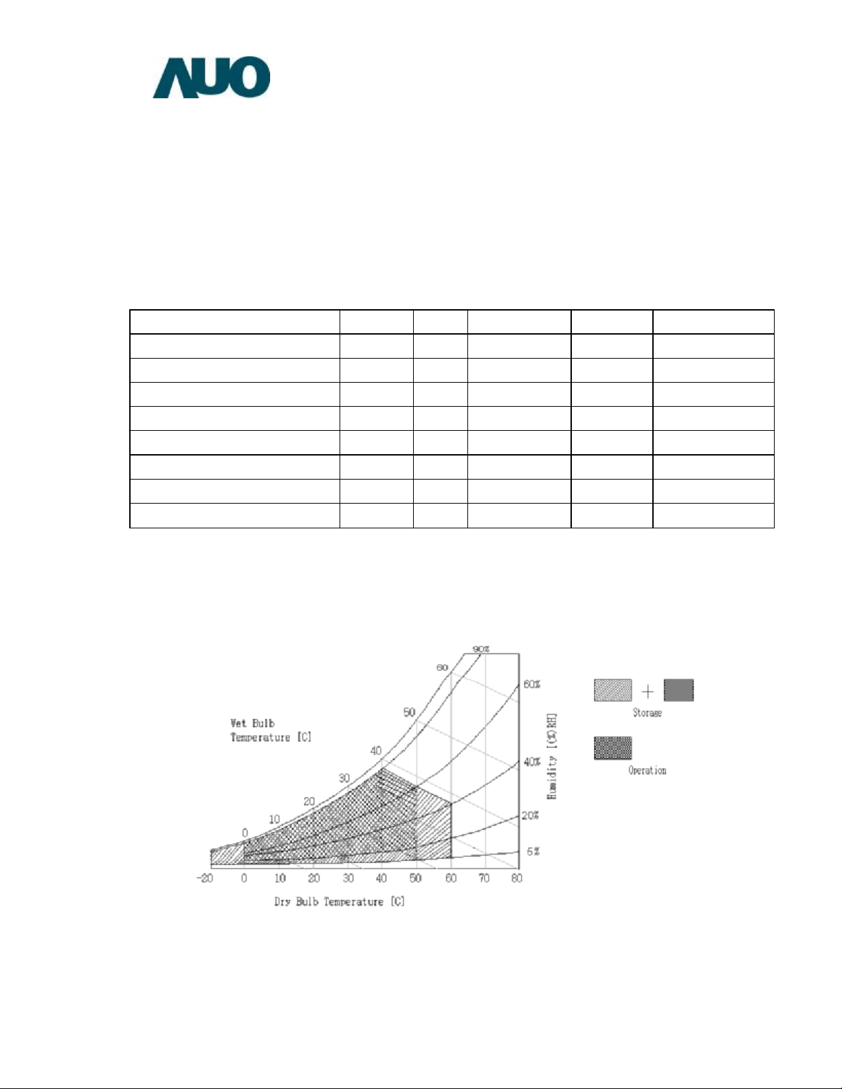
Operating Temperature TOP 0 +50 [
Operating Humidity HOP 10 90 [%RH] Note 2
Storage Temperature TST -20 +60 [
o
C] Note 2
o
C] Note 2
Storage Humidity HST 10 90 [%RH] Note 2
Note 1 : Duration = 50msec
Note 2 : Maximum Wet-Bulb should be 39℃ and No condensation.
Note 3 :The relative humidity must not exceed 90% non-condensing at temperatures of 40℃ or less. At
temperatures greater than 40℃, the wet bulb temperature must not exceed 39℃.
©Copyright AU Optronics, Inc.
January, 2003 All Rights Reserved. T315XW01 V5 - Specs. Ver 0.1 5/25
No Reproduction and Redistribution Allowed
3. Electrical Specification
The T315XW01 V2 requires two power inputs. One is employed to power the LCD electronics and to drive the
TFT array and liquid crystal. The second input power for the BLU, is to power inverter..
3-1 Electrical Characteristics
Values Parameter Symbol
Min Typ Max
LCD:
Power Supply Input Voltage Vcc 4.5 5.0 5.5 Vdc
Power Supply Input Current Icc - (1.5) (1.8) A 1
Unit Notes
Power Consumption Pc - (7.5)
Inrush Current I
Backlight Power Consumption Pbl (115) (132) Watt
Life Time 60,000 Hours 3
Note :
1. Vcc=5.0V, =
2. Duration = 1ms
3. The performance of the Lamp in LCM, for example life time or brightness, is extremely influenced by
the characteristics of the DC-AC Inverter. So all the parameters of an inverter should be carefully
designed so as not to produce too much leakage current from high-voltage output of the inverter. When
you design or order the inverter, please make sure unwanted lighting caused by the mismatch of the
lamp and the inverter (no lighting, flicker, etc) never occurs. When you confirm it, the LCD Assembly
should be operated in the same condition as installed in your instrument.
4. Do not attach a conducting tape to lamp connecting wire. If the lamp wire attach to conducting tape,
TFT-LCD Module have a low luminance and the inverter has abnormal action because leakage current
occurs between lamp wire and conducting tape.
5. The relative humidity must not exceed 80% non-condensing at temperatures of 40℃ or less. At
f 60Hz, fCLK=81.5Mhz , 25℃,
v
TBD - TBD Apeak 2
RUSH
(9)
Watt 1
temperatures greater than 40℃, the wet bulb temperature must not exceed 39℃. When operate at low
temperatures, the brightness of CCFL will drop and the life time of CCFL will be reduced.
©Copyright AU Optronics, Inc.
January, 2003 All Rights Reserved. T315XW01 V5 - Specs. Ver 0.1 6/25
No Reproduction and Redistribution Allowed
3-2 Interface Connections
- LCD connector (CN3): JAE FI-E30S or equivalent
- LVDS Transmitter: SN75LVDS83(Texas Instruments) or equivalent
Note:
All GND (ground) pins should be connected together and should also be connected to the LCD’s metal
1.
frame. All Vcc (power input) pins should be connected together.
No Signal No Signal
1 N.C. 16 GND
2 N.C. 17 RIN33 N.C. 18 RIN3+
4 GND 19 GND
5 RIN0- 20 Reserved.
6 RIN0+ 21 LVDS Option
7 GND 22 Reserved.
8 RIN1- 23 GND
9 RIN1+ 24 GND
10 GND 25 GND
11 RIN2- 26 Vdd (+5V)
12 RIN2+ 27 Vdd (+5V)
13 GND 28 Vdd (+5V)
14 RxCLK- 29 Vdd (+5V)
15 RxCLK+ 30 Vdd (+5V)
** LVDS Option : H (3.3V) or NCè NS
L (GND) è JEIDA
©Copyright AU Optronics, Inc.
January, 2003 All Rights Reserved. T315XW01 V5 - Specs. Ver 0.1 7/25
No Reproduction and Redistribution Allowed
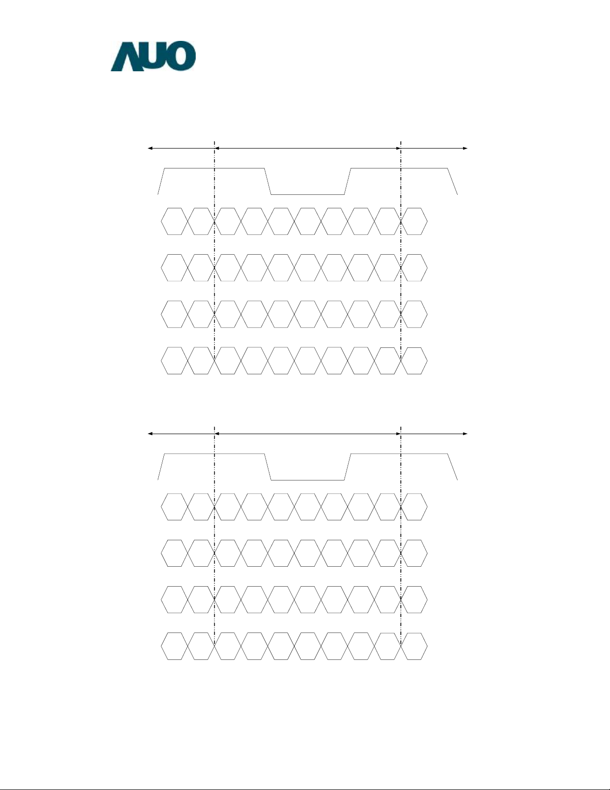
LVDS Option = L (GND)
Previous Cycle Current Cycle Next Cycle
Clock
RIN0+
RIN0-
RIN1+
RIN1-
RIN2+
RIN2-
RIN3+
RIN3-
LVDS Option = H (3.3V)
Previous Cycle Current Cycle Next Cycle
Clock
RIN0+
RIN0-
R2R7 G2G2R2R3 R4R5R6 R3
G3B2 B3B3G3G4 G5G6G6 G4
B4NA DEDEB4B5 B6B7NA B5
R0B1 NANAR0R1 G0G1B0 R1
R0R5 G0G0R0R1 R2R3R4 R1
RIN1+
RIN1-
RIN2+
RIN2-
RIN3+
RIN3-
G1B0 B1B1G1G2 G3G4G5 G2
B2NA DEDEB2B3 B4B5NA B4
R6B7 NANAR6R7 G6G7B6 R7
©Copyright AU Optronics, Inc.
January, 2003 All Rights Reserved. T315XW01 V5 - Specs. Ver 0.1 8/25
No Reproduction and Redistribution Allowed
 Loading...