

AUO T260XW02 VR Specification
Global LCD Panel Exchange Center
www.panelook.com
Product Description: T260XW02 TFT-LCD PANEL with RoHS Guarantee
AUO Model Name: T260XW02 VR
Customer Part No/Project Name:
Customer Signature Date AUO Date
Approved By: PM Director/ Frank Hsu
Reviewed By: RD Director/ Hong Hong Jye
Reviewed By: Project Leader/ Gavin Huang
Prepared By: PM/ Alvin Chung
Ϩ
Copyright AU Optronics, Inc.
January, 2003 All Rights Reserved. T260XW02 VR - Spec. Ver1.0
0/27
No Reproduction and Redistribution Allowed
One step solution for LCD / PDP / OLED panel application: Datasheet, inventory and accessory!
www.panelook.com
Global LCD Panel Exchange Center
www.panelook.com
Document Version: 1.0
Date: 2008/9/17
Product Specifications
26.0” WXGA Color TFT-LCD Module
Model Name: T260XW02 VR
(*) Preliminary Specifications
() Final Specifications
Ϩ
Copyright AU Optronics, Inc.
January, 2003 All Rights Reserved. T260XW02 VR - Spec. Ver1.0
1/27
No Reproduction and Redistribution Allowed
One step solution for LCD / PDP / OLED panel application: Datasheet, inventory and accessory!
www.panelook.com
Global LCD Panel Exchange Center
www.panelook.com
Contents
No
1
2
3
3-1
3-2
3-3
3-4
3-5
3-6
3-7
4
ITEM
COVER
CONTENTS
RECORD OF REVISIONS
GENERAL DESCRIPTION
ABSOLUTION MAXIMUM RATINGS
ELECTRICAL SPECIFICATIONS
ELECTRICAL CHARACTERISTICS
INTERFACE CONNECTIONS
SIGNAL TIMING SPECIFICATIONS
SIGNAL TIMING WAVEFORMS
COLOR INPUT DATA REFERENCE
POWER SEQUENCE for LCD
POWER SEQUENCE for INVERTER
OPTICAL SPECIFICATIONS
5
5-1
5-2
6
7
7-1
7-2
7-3
8
9
MECHANICAL CHARACTERISTICS
FRONT VIEW
REAR VIEW
RELIABILITY
INTERNATIONAL STANDARDS
SAFETY
EMC
GREEN
PACKING
PRECAUTIONS
Ϩ
Copyright AU Optronics, Inc.
January, 2003 All Rights Reserved. T260XW02 VR - Spec. Ver1.0
2/27
No Reproduction and Redistribution Allowed
One step solution for LCD / PDP / OLED panel application: Datasheet, inventory and accessory!
www.panelook.com
Global LCD Panel Exchange Center
www.panelook.com
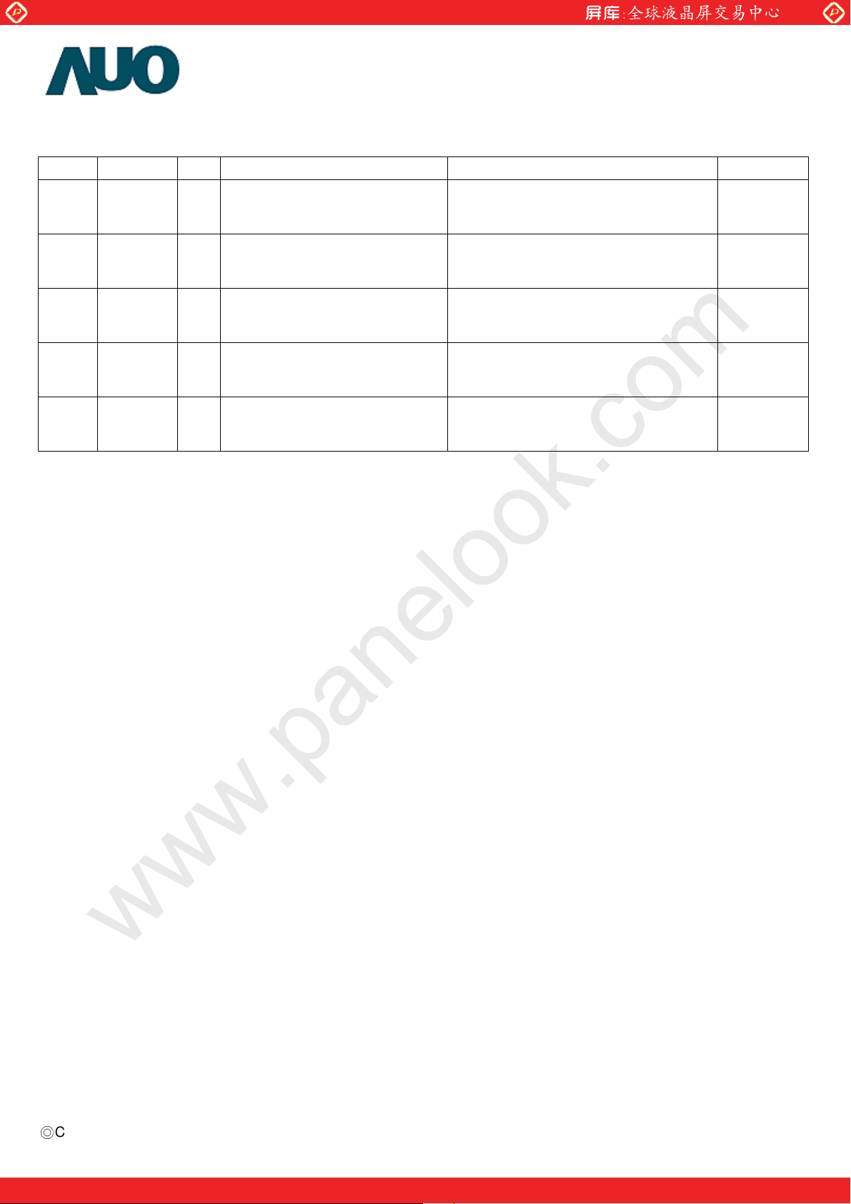
Record of Revision
Version Date No Old Description New Description Remark
1.0 2008/09/17 First release
Ϩ
Copyright AU Optronics, Inc.
January, 2003 All Rights Reserved. T260XW02 VR - Spec. Ver1.0
3/27
No Reproduction and Redistribution Allowed
One step solution for LCD / PDP / OLED panel application: Datasheet, inventory and accessory!
www.panelook.com
Global LCD Panel Exchange Center
www.panelook.com
1. General Description
This specification applies to the 26.0 inch Color TFT-LCD Module T260XW02 VR. This LCD
module has a TFT active matrix type liquid crystal panel 1366x768 pixels, and diagonal size of 26.0
inch. This module supports 1366x768 XGA-WIDE mode (Non-interlace).
Each pixel is divided into Red, Green and Blue sub-pixels or dots which are arranged in vertical
stripes. Gray scale or the brightness of the sub-pixel color is determined with a 8-bit gray scale
signal for each dot.
The T260XW02 VR has been designed to apply the 8-bit 1 channel LVDS interface method. It is
intended to support displays where high brightness, wide viewing angle, high color saturation, and
high color depth are very important. The T260XW02 VR model is RoHS verified which can be
distinguished on panel label.
* General Information
Items Specification Unit Note
Active Screen Size 26.0 inches
Display Area 575.769 (H) x 323.712(V) mm
Outline Dimension 626.0 (H) x 373.0 (V) x 45.0(D) mm With inverter
Driver Element a-Si TFT active matrix
Display Colors 16.7M Colors
Number of Pixels 1366 x 768 Pixel
Pixel Pitch 0.4215 mm
Pixel Arrangement RGB vertical stripe
Display Mode Normally Black
Surface Treatment AG, Haze=11%, 3H
Ϩ
Copyright AU Optronics, Inc.
January, 2003 All Rights Reserved. T260XW02 VR - Spec. Ver1.0
4/27
No Reproduction and Redistribution Allowed
One step solution for LCD / PDP / OLED panel application: Datasheet, inventory and accessory!
www.panelook.com
Global LCD Panel Exchange Center
www.panelook.com
2. Absolute Maximum Ratings
The following are maximum values which, if exceeded, may cause faulty operation or damage to
the unit.
Item Symbol Min Max Unit Conditions
-0.3 13.2 [Volt] Note 1
Logic/LCD Drive Voltage
Input Voltage of Signal
BLU Input Voltage
BLU Brightness Control Voltage
Operating Temperature
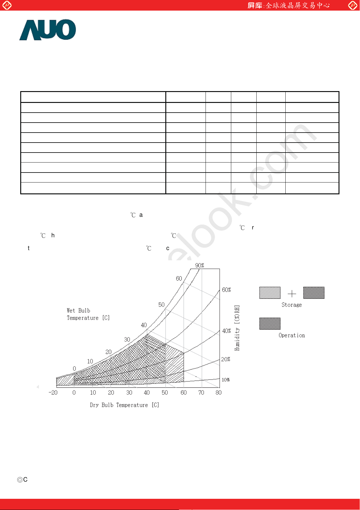
Operating Humidity
Storage Temperature
Storage Humidity
Panel Surface Temperature PST 65 [oC] Note 3
V
CC
-0.3 3.6 [Volt] Note 1
V
in
VDDB -0.3 27.0 [Volt] Note 1
VDIM -0.3 6.0 [Volt] Note 1
o
TOP 0 +50 [
C] Note 2
HOP 10 90 [%RH] Note 2
o
TST -20 +60 [
C] Note 2
HST 10 90 [%RH] Note 2
Note 1: Duration = 1 sec
к
Note 2: Maximum Wet-Bulb should be 39
The relative humidity must not exceed 90% non-condensing at temperatures of 40
than 40
Note 3: Surface temperature is measured at 50
к
, the wet bulb temperature must not exceed 39к.
and No condensation.
к
Dry condition
к
or less. At temperatures greater
Ϩ
Copyright AU Optronics, Inc.
January, 2003 All Rights Reserved. T260XW02 VR - Spec. Ver1.0
5/27
No Reproduction and Redistribution Allowed
One step solution for LCD / PDP / OLED panel application: Datasheet, inventory and accessory!
www.panelook.com
Global LCD Panel Exchange Center
www.panelook.com
3. Electrical Specification
The T260XW02 VR requires two power inputs. One is employed to power the LCD electronics and
to drive the TFT array and liquid crystal. The second input power for the BLU is to power inverter.
3-1 Electrical Characteristics
Parameter Symbol
Min Typ Max
LCD:
Power Supply Input Voltage Vcc 10.8 12 13.2 Vdc 1
Power Supply Input Current Icc - 0.35 A 2
Power Consumption Pc - 4.2 Watt 2
Inrush Current I
- - 3.0 Apeak 3
RUSH
Values
Unit Notes
LVDS
Interface
CMOS
Interface
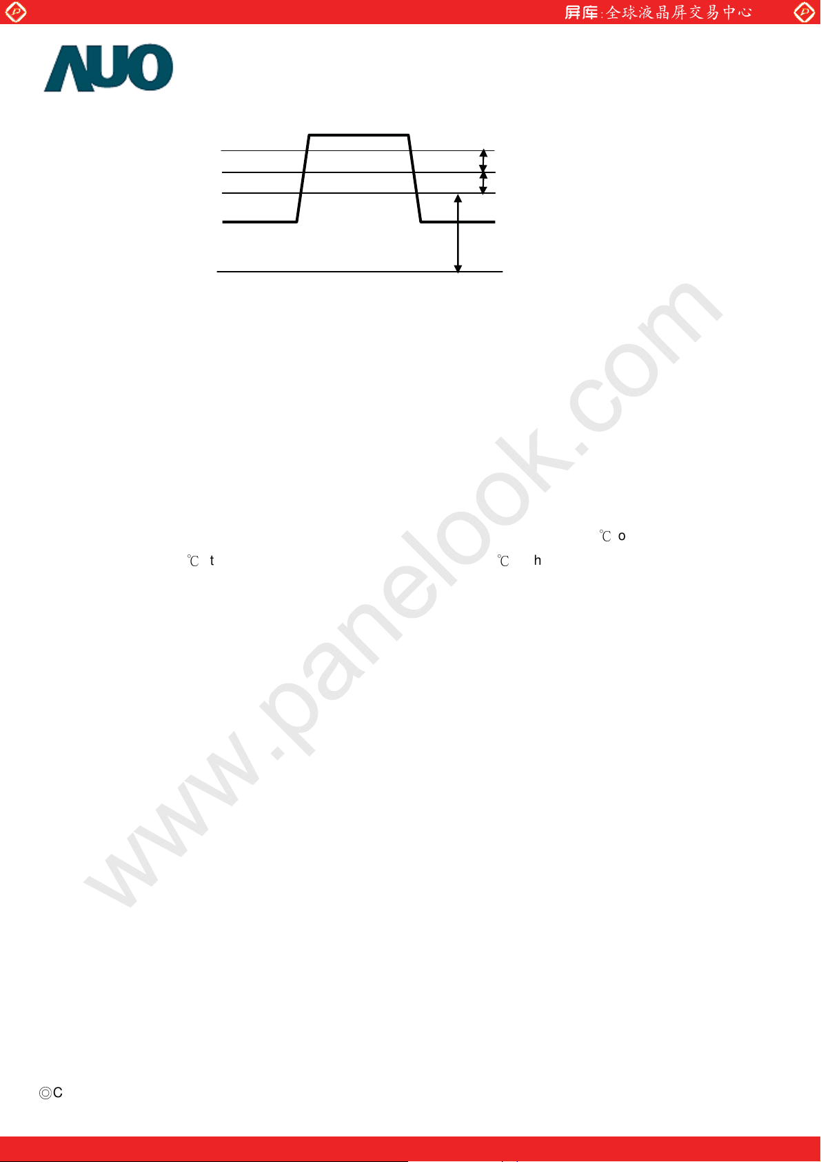
Differential Input High
Threshold Voltage
Differential Input Low
Threshold Voltage
Common Input
Voltage
Input High Threshold
Voltage
Input Low Threshold
Voltage
VTH +100 mV 4
VTL -100 mV 4
VCIM 1.10 1.25 1.40 V 4
VIH
(High)
VIL
(Low)
2.4 3.3 Vdc
0 0.7 Vdc
Backlight Power Consumption PDDB 40 Watt 8
Life Time 50,000 60,000 Hours 9
Note :
1. The ripple voltage should be controlled under 10% of V
=
f
2. Vcc=12.0V,
3. Measurement condition :
60Hz, fCLK=81.5Mhz , 25к, Test Pattern : White Pattern
v
CC
Ϩ
Copyright AU Optronics, Inc.
January, 2003 All Rights Reserved. T260XW02 VR - Spec. Ver1.0
6/27
No Reproduction and Redistribution Allowed
One step solution for LCD / PDP / OLED panel application: Datasheet, inventory and accessory!
www.panelook.com
Global LCD Panel Exchange Center
4. VCIM = 1.2V
www.panelook.com
VCIM
VTH
VIL
0V
5. The performance of the Lamp in LCM, for example life time or brightness, is extremely influenced by the
characteristics of the DC-AC Inverter. So all the parameters of an inverter should be carefully designed so as
not to produce too much leakage current from high-voltage output of the inverter. W hen you design or order
the inverter, please make sure unwanted lighting caused by the mismatch of the lamp and the inverter (no
lighting, flicker, etc) never occurs. When you confirm it, the LCD Assembly should be operated in the same
condition as installed in your instrument.
6. Do not attach a conducting tape to lamp connecting wire. If the lamp wire attach to conducting tape, TFT-LCD
Module have a low luminance and the inverter has abnormal action because leakage current occurs between
lamp wire and conducting tape.
7. The relative humidity must not exceed 80% non-condensing at temperatures of 40
greater than 40
к
, the wet bulb temperature must not exceed 39к. When operate at low temperatures, the
к
or less. At temperatures
brightness of CCFL will drop and the life time of CCFL will be reduced.
Ϩ
Copyright AU Optronics, Inc.
January, 2003 All Rights Reserved. T260XW02 VR - Spec. Ver1.0
7/27
No Reproduction and Redistribution Allowed
One step solution for LCD / PDP / OLED panel application: Datasheet, inventory and accessory!
www.panelook.com
Global LCD Panel Exchange Center
www.panelook.com
3-2 Interface Connections
LCD connector (CN1): Starconn 093G30-B0001A-1
Pin No Symbol Description Default
1 VCC +12V, DC, Regulated
2 VCC +12V, DC, Regulated
3 VCC +12V, DC, Regulated
4 VCC +12V, DC, Regulated
5 GND Ground and Signal Return
6 GND Ground and Signal Return
7 GND Ground and Signal Return
8 GND Ground and Signal Return
9 LVDS Option Low/Open for Normal (NS), High for JEIDA
10 Reserved Open or High
11 GND Ground and Signal Return for LVDS
12 RIN0- LVDS Channel 0 negative
13 RIN0+ LVDS Channel 0 positive
14 GND Ground and Signal Return for LVDS
15 RIN1- LVDS Channel 1 negative
16 RIN1+ LVDS Channel 1 positive
17 GND Ground and Signal Return for LVDS
18 RIN2- LVDS Channel 2 negative
19 RIN2+ LVDS Channel 2 positive
20 GND Ground and Signal Return for LVDS
21 RCLK- LVDS Clock negative
22 RCLK+ LVDS Clock positive
23 GND Ground and Signal Return for LVDS
24 RIN3- LVDS Channel 3 negative
25 RIN3+ LVDS Channel 3 positive
26 GND Ground and Signal Return for LVDS
27 Reserved Open or High
28 Reserved Open or High
29 GND Ground and Signal Return
30 GND Ground and Signal Return
NS Mode
AUO internal test
AUO internal test
AUO internal test
Note:
1. All GND (ground) pins should be connected together and should also be connected to the LCD’s metal frame.
2. All Vcc (power input) pins should be connected together.
Ϩ
Copyright AU Optronics, Inc.
January, 2003 All Rights Reserved. T260XW02 VR - Spec. Ver1.0
8/27
No Reproduction and Redistribution Allowed
One step solution for LCD / PDP / OLED panel application: Datasheet, inventory and accessory!
www.panelook.com
 Loading...