

AUO T260XW02 V2 Specification

Global LCD Panel Exchange Center
www.panelook.com
Document Version: 2.3
Date: 2005/10/13
Product Specifications
26.0” WXGA Color TFT-LCD Module
Model Name: T260XW02
(*) Preliminary Specifications
( ) Final Specifications
Copyright AU Optronics, Inc.
January, 2003 All Rights Reserved. T260XW02 V2-Spec. Ver2.3 1/26
PDF created with FinePrint pdfFactory Pro trial version http://www.fineprint.com
One step solution for LCD / PDP / OLED panel application: Datasheet, inventory and accessory!
www.panelook.com
Global LCD Panel Exchange Center
No ITEM
COVER
CONTENTS
RECORD OF REVISIONS
www.panelook.com
Contents
1
2
3
4
5
6
7
8
9
3-1
3-2
3-3
3-4
3-5
3-6
7-1
7-2
GENERAL DESCRIPTION
ABSOLUTION MAXIMUM RATINGS
ELECTRICAL SPECIFICATIONS
ELECTRICAL CHARACTERISTICS
INTERFACE CONNECTIONS
SIGNAL TIMING SPECIFICATIONS
SIGNAL TIMING WAVEFORMS
COLOR INPUT DATA REFERENCE
POWER SEQUENCE
OPTICAL SPECIFICATIONS
MECHANICAL CHARACTERISTICS
RELIABILITY
INTERNATIONAL STANDARDS
SAFETY
EMC
PACKING
PRECAUTIONS
Copyright AU Optronics, Inc.
January, 2003 All Rights Reserved. T260XW02 V2-Spec. Ver2.3 2/26
PDF created with FinePrint pdfFactory Pro trial version http://www.fineprint.com
One step solution for LCD / PDP / OLED panel application: Datasheet, inventory and accessory!
www.panelook.com
Global LCD Panel Exchange Center
Version Date No Old Description New Description Remark
0 6/14 ‘05
2.1 7/13 ‘05
2.2 8/17 ‘05
2.3 10/13 ‘05
Original version
Optical Specification:
Response timeRise time: T
=12ms
T
rD
Mechanical Characteristics:
Bezel AreaHorizontal=580.0mm
2. Absolute Maximum Ratings
Symbol: VDD
Note1: Duration = 50msec
Symbol Min Max Unit
V
Vin -0.3 (3.6) [Volt]
VDDB -0.3 27. 0 [Volt]
BLON -0.3 7.0 [Volt]
TOP 0 +50 [oC]
HOP 10 90 [%RH]
TST -20 +60 [oC]
HST 10 90 [%RH]
** LVDS Option :
H (3.3V) or N.C. NS (Normal)
L (GND) JETDA
** Rotate Option : H (3.3V) U/D,
R/L rotate
L (GND) Normal
Input Current
=3.95A(max.)
I
DDB
Input Power
=85W(max.)
P
DDB
Signal Item Symbol Min. Typ. Max. Unit
Period Tv 789 806 822 Th
Vertical
Active Tdisp 768 Th
Section
Blanking Tblk (v) 21 38 54 Th
Period Th 1414 1560 1722 Tcl k
Horizontal
Active Tdisp 1366 Tclk
Section
Blanking Tblk( h) 48 194 356 Tclk
Clock Frequency Fclk 65 76 88 MHz
Vertical
Frequency Fv 58 60 62 Hz
Frequency
Horizontal
Frequency Freq 47.32 --- 49.32 kHz
Frequency
Record of Revision
Decay time:
Vertical=328.0mm
-0.3 (7.0) [Volt ]
CC
www.panelook.com
=12ms
rR
Optical Specification:
Response timeRise time: T
Mechanical Characteristics:
Bezel AreaHorizontal=580.8mm
2. Absolute Maximum Ratings
Symbol: VDDB
Note 1 : Duration = 1 sec
Symbol Min Max Unit
V
VDDB -0.3 27.0 [Volt]
BLON -0.3 7.0 [Volt]
VDIM -0.3 6.0 [Volt]
V
EV
** LVDS Option :
H (3.3V) or N.C. NS (Normal)
L (GND) JETDA
Input Current (Turn on Condition)
I
=3.65A(typ.)
DDB
=3.95A(max.)
I
DDB
Input Power (Turn on Condition)
=87.6W(typ.)
P
DDB
=94.8W(max.)
P
DDB
Input Current (Stable Condition)
=3.5A(typ.)
I
DDB
=3.6A(max.)
I
DDB
Input Power (Stable Condition)
=84W(typ.)
P
DDB
=87W(max.)
P
DDB
Signal Item Symbol Min. Typ. Max. Unit
Vertical
Section
Horizontal
Section
Clock Frequency Fclk 80 84 88 MHz
Vertical
Frequency
Horizontal
Frequency
=8ms
rR
Decay time: T
rD
=8ms
Vertical=328.8mm
V
-0.3 (6.0) [Volt]
CC
-0.3 (3.6) [Volt]
LVDSOPT
-0.3 6.0 [Volt]
BLON
-0.3 6.0 [Volt]
PWM
TOP 0 +50 [oC]
HOP 10 90 [%RH]
TST -20 +60 [oC]
HST 10 90 [%RH]
Period Tv 950 975 1000 Th
Active Tdi sp 768
Blanking Tblk (v) 182 207 232 Th
Period Th 1414 1435 1543 Tclk
Active Tdi sp 1366
Blanking Tblk (h) 48 69 177 Tclk
Frequency Fv -- 60 -- Hz
Frequency Freq 57 --- 60 kHz
Page 15
Page 18
Page 5
Page7,8
Page 9
Page 11
Copyright AU Optronics, Inc.
January, 2003 All Rights Reserved. T260XW02 V2-Spec. Ver2.3 3/26
PDF created with FinePrint pdfFactory Pro trial version http://www.fineprint.com
One step solution for LCD / PDP / OLED panel application: Datasheet, inventory and accessory!
www.panelook.com
Global LCD Panel Exchange Center
www.panelook.com
1. General Description
This specification applies to the 26.0 inch Color TFT-LCD Module T260XW02. This LCD module has a TFT
active matrix type liquid crystal panel 1366x768 pixels, and diagonal size of 26.0 inch. This module supports
1366x768 XGA-WIDE mode (Non-interlace).
Each pixel is divided into Red, Green and Blue sub-pixels or dots which are arranged in vertical stripes. Gray
scale or the brightness of the sub-pixel color is determined with a 8-bit gray scale signal for each dot.
The T260XW02 has been designed to apply the 8-bit 1 channel LVDS interface method. It is intended to
support displays where high brightness, wide viewing angle, high color saturation, and high color depth are
very important.
* General Information
Items Specification Unit Note
Active Screen Size
Display Area
Pixel Pitch
Outline Dimension
Driver Element
Display Colors
Number of Pixels
Pixel Arrangement
Display Mode
BL Structure
Surface Treatment
26.0
575.769 (H) x 323.712(V)
0.4215 mm
626.0 (H) x 373.0 (V) x 47.5(D)
a-Si TFT active matrix
16.7M
1366 x 768
RGB vertical stripe
Normally Black
8 U-Lamps
AG, 3H
inches
mm
mm With inverter
Colors
Pixel
Copyright AU Optronics, Inc.
January, 2003 All Rights Reserved. T260XW02 V2-Spec. Ver2.3 4/26
PDF created with FinePrint pdfFactory Pro trial version http://www.fineprint.com
One step solution for LCD / PDP / OLED panel application: Datasheet, inventory and accessory!
www.panelook.com
Global LCD Panel Exchange Center
www.panelook.com
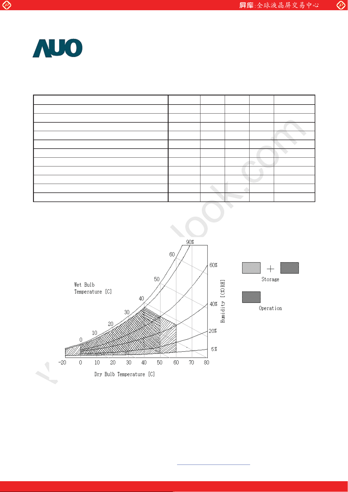
2. Absolute Maximum Ratings
The following are maximum values which, if exceeded, may cause faulty operation or damage to the unit.
Item Symbol Min Max Unit Conditions
Logic/LCD Drive Voltage
LVDS Option Control Voltage
BLU Input Voltage
BLU Brightness Control Voltage
External Analog Dimming Control Voltage
On/Off Control Voltage
External PWM Dimming Control Voltage
Operating Temperature
Operating Humidity
Storage Temperature
Storage Humidity
V
CC
V
LVDSOPT
VDDB -0.3 27.0 [Volt] Note 1
BLON -0.3 7.0 [Volt] Note 1
VDIM -0.3 6.0 [Volt] Note 1
V
BLON
EV
PWM
TOP 0 +50 [oC] Note 2
HOP 10 90 [%RH] Note 2
TST -20 +60 [oC] Note 2
HST 10 90 [%RH] Note 2
-0.3 (6.0) [Volt] Note 1
-0.3 (3.6) [Volt] Note 1
-0.3 6.0 [Volt] Note 1
-0.3 6.0 [Volt] Note 1
Note 1 : Duration = 1sec
Note 2 : Maximum Wet-Bulb should be 39 and No condensation.
Copyright AU Optronics, Inc.
January, 2003 All Rights Reserved. T260XW02 V2-Spec. Ver2.3 5/26
PDF created with FinePrint pdfFactory Pro trial version http://www.fineprint.com
One step solution for LCD / PDP / OLED panel application: Datasheet, inventory and accessory!
www.panelook.com
Global LCD Panel Exchange Center
s
μ
www.panelook.com
3. Electrical Specification
The T260XW02 requires two power inputs. One is employed to power the LCD electronics and to drive the
TFT array and liquid crystal. The second input power for the BLU, is to power inverter..
3-1 Electrical Characteristics
Parameter
Symbol
Min. Typ. Max.
Values
Unit Notes
LCD:
Power Supply Input Voltage
Power Supply Input Current
Power Consumption
Inrush Current
V
cc
Icc - 1.40 1.78 A 1
Pc - 7.0 9.0 Watt 1
I
RUSH
Backlight Power Consumption
Life Time
Note :
1.
Vcc=5.0V, Fv=60Hz, Fclk= 85.0 MHz , 25.
2.
Vcc rising time = 470
3.
The performance of the Lamp in LCM, for example: lifetime or brightness, is extremely influenced by the characteristics
of the DC-AC Inverter. So all the parameters of an inverter should be carefully designed so as not to produce too much
leakage current from high-voltage output of the inverter. When you design or order the inverter, please make sure
unwanted lighting caused by the mismatch of the lamp and the inverter (no lighting, flicker, etc) never occurs. When you
confirm it, the LCD Assembly should be operated in the same condition as installed in your instrument.
4.
Do not attach a conducting tape to lamp connecting wire. If the lamp wire attach to conducting tape, TFT-LCD Module
have a low luminance and the inverter has abnormal action because leakage current occurs between lamp wire and
conducting tape.
5.
The relative humidity must not exceed 80% non-condensing at temperatures of 40or less. At temperatures greater than
40, the wet bulb temperature must not exceed 39. When operate at low temperatures, the brightness of CCFL will
drop and the lifetime of CCFL will be reduced.
, Vcc=5.0V
4.5 5.0 5.5 V
- - 3.0 A 2
- - 94.8 Watt 3
50,000 60,000 Hours 4
Copyright AU Optronics, Inc.
January, 2003 All Rights Reserved. T260XW02 V2-Spec. Ver2.3 6/26
PDF created with FinePrint pdfFactory Pro trial version http://www.fineprint.com
One step solution for LCD / PDP / OLED panel application: Datasheet, inventory and accessory!
www.panelook.com
Global LCD Panel Exchange Center
3-2 Interface Connections
LCD connector (CN1): JAE FI-E30S or equivalent
-
- Mating Connector:
- LVDS Transmitter: SN75LVDS83(Texas Instruments) or equivalent
Note:
1.
All GND (ground) pins should be connected together and should also be connected to the LCD’s metal frame. All Vcc
(power input) pins should be connected together.
Pin No Symbol Description Default
1 N.C. No Connection ( Auo internal Test Pin)
2 N.C. No Connection ( Auo internal Test Pin)
3 N.C. No Connection ( Auo internal Test Pin)
4 GND Power Ground
5 Rx0- Negative LVDS differential data input
6 Rx0+ Positive LVDS differential data input
7 GND Power Ground
8 Rx1- Negative LVDS differential data input
9 Rx1+ Positive LVDS differential data input
10 GND Power Ground
11 Rx2- Negative LVDS differential data input
12 Rx2+ Positive LVDS differential data input
13 GND Power Ground
14 RxCLK- Negative LVDS differential clock input
15 RxCLK+ Positive LVDS differential clock input
16 GND Power Ground
17 Rx3- Negative LVDS differential data input
18 Rx3+ Positive LVDS differential data input
19 GND Power Ground
20 N.C. No Connection ( Auo internal Test Pin)
21 LVDS Option Pull Low : JETDA LVDS format; Pull High or N.C.: NS LVDS format
22 N.C. No Connection ( Auo internal Test Pin)
23 GND Power Ground
24 GND Power Ground
25 GND Power Ground
26 V
27 V
28 V
29 V
30 V
** LVDS Option : H (3.3V) or N.C.
CC
CC
CC
CC
CC
L (GND)
JETDA
+5V Power Input
+5V Power Input
+5V Power Input
+5V Power Input
+5V Power Input
NS
www.panelook.com
Copyright AU Optronics, Inc.
January, 2003 All Rights Reserved. T260XW02 V2-Spec. Ver2.3 7/26
PDF created with FinePrint pdfFactory Pro trial version http://www.fineprint.com
One step solution for LCD / PDP / OLED panel application: Datasheet, inventory and accessory!
www.panelook.com
Global LCD Panel Exchange Center
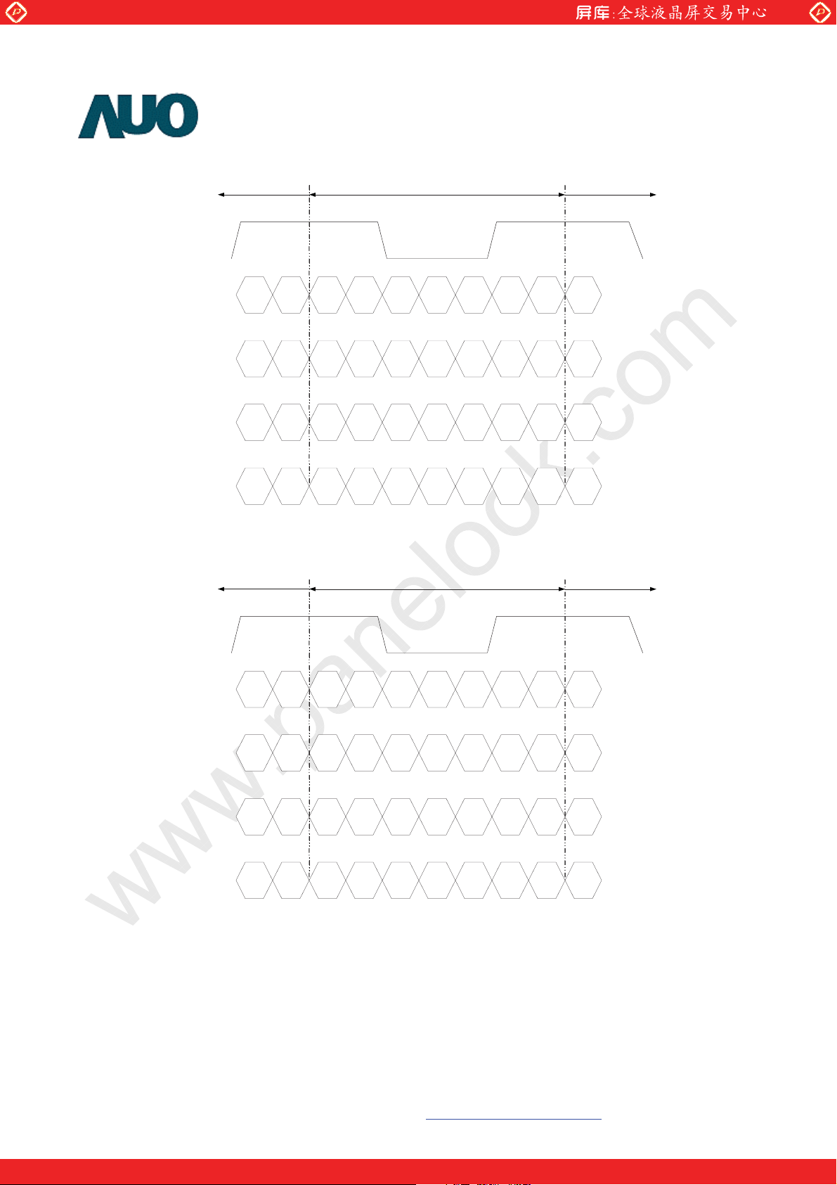
LVDS Option = L (GND)JETDA Format
Previous Cycle Current Cycle Next Cycle
Clock
www.panelook.com
RIN0+
RIN0-
RIN1+
RIN1-
RIN2+
RIN2-
RIN3+
RIN3-
LVDS Option = H (3.3V) or N.C.NS Format
Previous Cycle Current Cycle Next Cycle
Clock
RIN0+
RIN0-
R2R7 G2G2R2R3 R4R5R6 R3
G3B2 B3B3G3G4 G5G6G6 G4
B4NA DEDEB4B5 B6B7NA B5
R0B1 NANAR0R1 G0G1B0 R1
R0R5 G0G0R0R1 R2R3R4 R1
RIN1+
RIN1-
RIN2+
RIN2-
RIN3+
RIN3-
G1B0 B1B1G1G2 G3G4G5 G2
B2NA DEDEB2B3 B4B5NA B4
R6B7 NANAR6R7 G6G7B6 R7
Copyright AU Optronics, Inc.
January, 2003 All Rights Reserved. T260XW02 V2-Spec. Ver2.3 8/26
PDF created with FinePrint pdfFactory Pro trial version http://www.fineprint.com
One step solution for LCD / PDP / OLED panel application: Datasheet, inventory and accessory!
www.panelook.com
 Loading...