

AUO T260HW01 V0 Specification
T260HW01 V0 SKD Product Specification
_____________________________________
Rev 1.0
Model Name: T260HW01 V0 SKD
Issue Date : 2013/6/14
( )Preliminary Specifications
(****)Final Specifications
Customer Signature Date AUO Date
Approved By
_________________________________
Note
Approval By PM Director
____________________________________
Reviewed By RD Director
____________________________________
Reviewed By Project Leader
Prepared By PM
© Copyright AU Optronics Corp. 2013 All Rights Reserved. Page 1 / 25
____________________________________
CONTENTS
T260HW01 V0 SKD Product Specification
Rev 1.0
1. GENERAL DESCRIPTION ............................................................................................................................................4
2. ABSOLUTE MAXIMUM RATINGS .............................................................................................................................5
3. ELECTRICAL SPECIFICATION..................................................................................................................................6
3.1
E
LECTRICAL CHARACTERISTICS
3.1.1 DC Characteristics .............................................................................................................................................6
3.1.2 AC Characteristics .............................................................................................................................................7
3.1.3 DRIVER CHARACTERISTICS ......................................................................................................................7
3.2
I
NTERFACE CONNECTIONS
3.2.1 T-Con Board Pin Map...................................................................................................................................... 11
3.2.2 LVDS Option.....................................................................................................................................................12
3.3
S
IGNAL TIMING SPECIFICATION
3.4
S
IGNAL TIMING WAVEFORMS
3.5
C
OLOR INPUT DATA REFERENCE
3.6
P
OWER SEQUENCE FOR
4. OPTICAL SPECIFICATION........................................................................................................................................17
LCD.................................................................................................................................16
.............................................................................................................................6
.....................................................................................................................................11
............................................................................................................................13
.................................................................................................................................14
...........................................................................................................................15
5. MECHANICAL CHARACTERISTICS.......................................................................................................................21
6. PACKING........................................................................................................................................................................22
7. PRECAUTIONS .............................................................................................................................................................24
7.1
M
7.2
7.3
7.4
7.5
7.6
OUNTING PRECAUTIONS
O
PERATING PRECAUTIONS
E
LECTROSTATIC DISCHARGE CONTROL
P
RECAUTIONS FOR STRONG LIGHT EXPOSURE
S
TORAGE
H
ANDLING PRECAUTIONS FOR PROTECTION FILM OF POLARIZER
.................................................................................................................................................................25
.....................................................................................................................................24
.....................................................................................................................................24
...............................................................................................................24
.....................................................................................................25
.....................................................................25
© Copyright AU Optronics Corp. 2013 All Rights Reserved. Page 2 / 25
RECORD OF REVISION
T260HW01 V0 SKD Product Specification
Rev 1.0
Version
1.0 2013/6/14 First release
Date Page Description
© Copyright AU Optronics Corp. 2013 All Rights Reserved. Page 3 / 25

T260HW01 V0 SKD Product Specification
Rev 1.0
1. General Description
This specification applies to the 26.0 inch Color TFT-LCD SKD model T260HW01 V0. This Open Cell Unit has a
TFT active matrix type liquid crystal panel 1920x1080 pixels, and diagonal size of 26.0 inch. This Open Cell Unit
supports 1920x1080 mode. Each pixel is divided into Red, Green and Blue sub-pixels or dots which are arranged
in vertical stripes. Gray scale or the brightness of the sub-pixel color is determined with a 8-bit gray scale signal for
each dot.
* General Information
Items Specification Unit Note
Active Screen Size 26.02 inch
Display Area 576.0 (H) x 324.0 (V) mm
Outline Dimension 599.32 (H) X363.56 (V) x 1.82 (D) mm D: cell thickness
Driver Element a-Si TFT active matrix
Display Colors 8 bit, 16.7M Colors
Number of Pixels 1,920x1,080 Pixel
Pixel Pitch 0.3 (H) x 0.3 (W) mm
Pixel Arrangement RGB Horizontal stripe
Display Operation Mode Normally Black
Surface Treatment Anti-Glare, 3H Haze=11%
Weight 0.7kg g
Rotate Function Unachievable Note 1
Display Orientation Signal input with “ABC” Note 2
Note 1: Rotate Function refers to LCD display could be able to rotate.
Note 2: LCD display as below illustrated when signal input with “ABC”.
© Copyright AU Optronics Corp. 2013 All Rights Reserved. Page 4 / 25
T260HW01 V0 SKD Product Specification
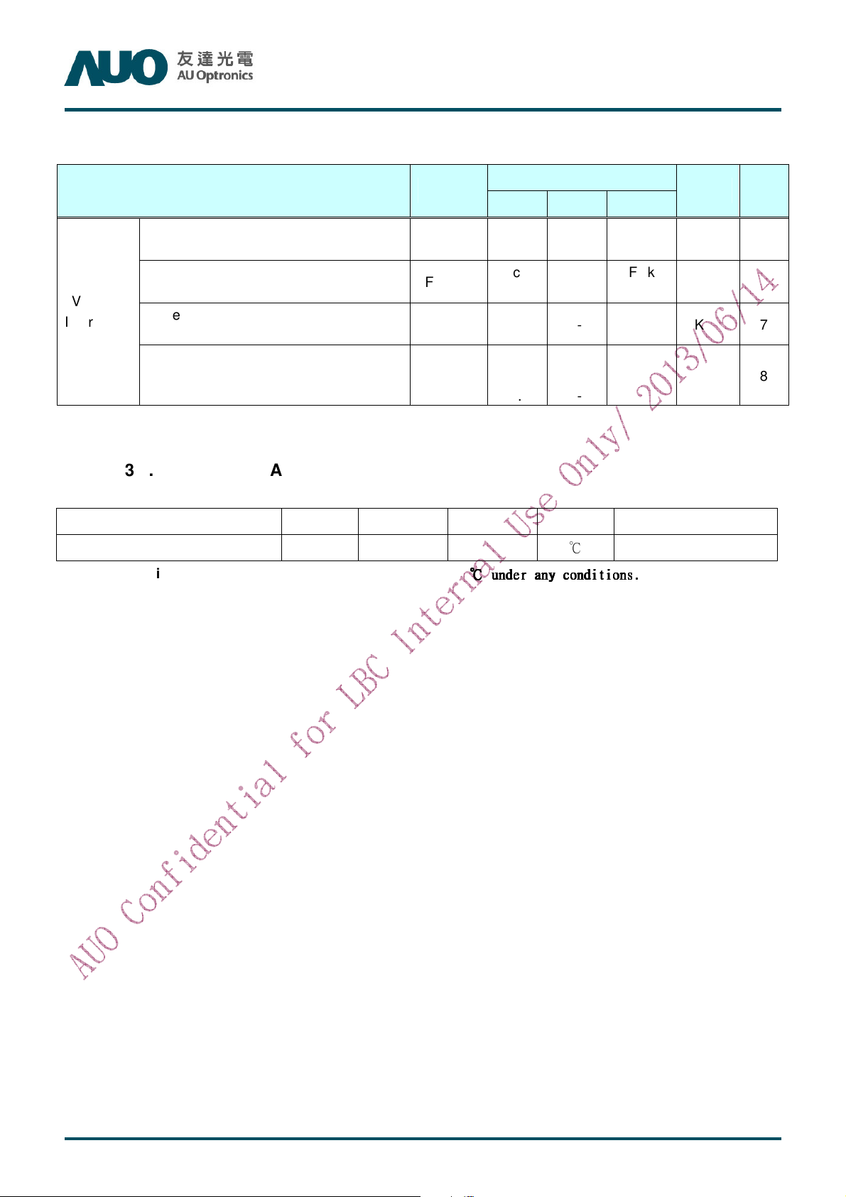
2. Absolute Maximum Ratings
The followings are maximum values which, if exceeded, may cause faulty operation or damage to the unit
Item Symbol Min Max Unit Conditions
Rev 1.0
Logic/LCD Drive Voltage VDD -0.3 14 [Volt]
Input Voltage of Signal Vin -0.3 4 [Volt]DC Note 1
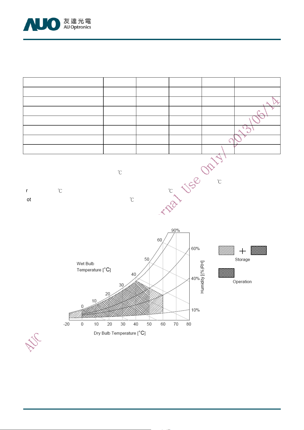
Operating Temperature TOP 0 +50 [oC] Note 2
Operating Humidity HOP 10 90 [%RH] Note 2
Storage Temperature TST -20 +60 [oC] Note 2
Storage Humidity HST 10 90 [%RH] Note 2
Panel Surface Temperature PST 65 [oC] Note 3
Note 1: Duration: 50 sec.
Note 2 : Maximum Wet-Bulb should be 39 and No condensation.℃
The relative humidity must not exceed 90% non-condensing at temperatures of 40 or less. At temperatures
greater than 40 , the wet bulb temperature must not exceed 39 .
Note 3: Surface temperature is measured at 50℃ Dry condition
℃ ℃
Note 1
DC
℃
© Copyright AU Optronics Corp. 2013 All Rights Reserved. Page 5 / 25
T260HW01 V0 SKD Product Specification
Rev 1.0
3. Electrical Specification
The T260HW01 V0 Open Cell Unit requires power input which is employed to power the LCD electronics and to
drive the TFT array and liquid crystal.
3.1 Electrical Characteristics
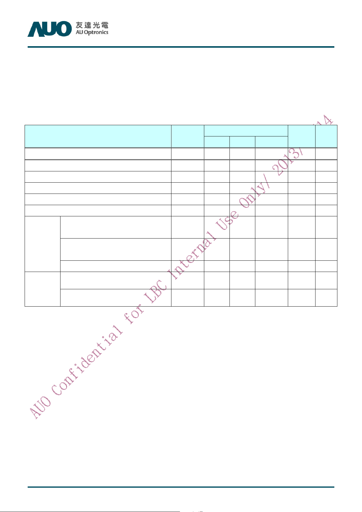
3.1.1 DC Characteristics
Parameter Symbol
LCD
Power Supply Input Voltage VDD 10.8 12 13.2 VDC
Power Supply Input Current IDD -- 0.52 0.57 A 1
Power Consumption PC -- 6.24 6.84 Watt 1
Inrush Current I
Permissible Ripple of Power Supply Input Voltage
Differential Input High Threshold
LVDS
Interface
CMOS
Interface
Voltage
Differential Input Low Threshold
Voltage
Input Common Mode Voltage V
Input High Threshold Voltage
Input Low Threshold Voltage
RUSH
VRP -- -- VDD * 5% mV
VTH -- -- +100 mVDC 4
VTL -100 -- -- mVDC 4
ICM
VIH
(High)
VIL
(Low)
Min. Typ. Max
-- -- 4 A 2
1.1 1.25 1.4 VDC 4
2.7 -- 3.3 VDC 5
0 -- 0.6 VDC 5
Value
Unit Note
pk-pk
3
© Copyright AU Optronics Corp. 2013 All Rights Reserved. Page 6 / 25
T260HW01 V0 SKD Product Specification
Rev 1.0
3.1.2 AC Characteristics
Parameter Symbol
LVDS
Interface
Input Channel Pair Skew Margin
(only for TCON: 12403U1, 12405)
Receiver Clock : Spread Spectrum
Modulation range
Receiver Clock : Spread Spectrum
Modulation frequency
Receiver Data Input Margin
Fclk = 85 MHz
Fclk = 65 MHz
t
SKEW (CP)
Fclk_ss
Fss
tRMG
3.1.3 DRIVER CHARACTERISTICS
Item Symbol Min Max Unit condition
Driver Surface Temperature DST 100
Note : Any point on the driver surface must be less than 100
Value
Min. Typ. Max
-500 -- +500 ps 6
Fclk
-3%
30
-0.4
-0.5
℃℃℃℃ under any conditions.
under any conditions.
under any conditions. under any conditions.
--
--
--
--
[℃]
Fclk
+3%
200
0.4
0.5
Note
Unit Note
MHz
7
KHz
7
ns
8
© Copyright AU Optronics Corp. 2013 All Rights Reserved. Page 7 / 25
Note :
s
µ
1. Test Condition:
(1) V
= 12.0V
DD
(2) Fv =60Hz
(3) Fclk= Max freq.
(4) Temperature = 25 ℃
(5) Typ. Input current : White Pattern
2. Measurement condition : Rising time = 400us
T260HW01 V0 SKD Product Specification
VVVV
DD
DD
90%
DDDD
Rev 1.0
GND
GND
GNDGND
10%
3. Test Condition:
(1) The measure point of V
is in LCM side after connecting the System Board and LCM.
RP
(2) Under Max. Input current spec. condition.
4. V
= 1.25V
ICM
L VD S -
V
IC M
L VD S +
G ND
0 V
400
400
400400
|VID|
V
T H
|VID|
V
T L
|VID|
5. The measure points of V
© Copyright AU Optronics Corp. 2013 All Rights Reserved. Page 8 / 25
and V
IH
are in LCM side after connecting the System Board and LCM.
IL
 Loading...