

Page 1

Contents
Revision History . . . . . . . . . . . . . . . . . . . . . . . . . . . . . . . . . . . . . . . . . . . . . . . . . . . . . . . . . . . . . . . 3
Preface . . . . . . . . . . . . . . . . . . . . . . . . . . . . . . . . . . . . . . . . . . . . . . . . . . . . . . . . . . . . . . . . . . . . . . . . 5
The Manual . . . . . . . . . . . . . . . . . . . . . . . . . . . . . . . . . . . . . . . . . . . . . . . . . . . . . . . . 5
Name Conventions . . . . . . . . . . . . . . . . . . . . . . . . . . . . . . . . . . . . . . . . . . . . . . . . . 5
Problem? . . . . . . . . . . . . . . . . . . . . . . . . . . . . . . . . . . . . . . . . . . . . . . . . . . . . . . . . . . 5
Contents - Packing List . . . . . . . . . . . . . . . . . . . . . . . . . . . . . . . . . . . . . . . . . . . . . . 5
Utility Disks . . . . . . . . . . . . . . . . . . . . . . . . . . . . . . . . . . . . . . . . . . . . . . . . . . . . . . . 6
Anti-Static Handling . . . . . . . . . . . . . . . . . . . . . . . . . . . . . . . . . . . . . . . . . . . . . . . . 6
Electromagnetic Compatibility (EMC) . . . . . . . . . . . . . . . . . . . . . . . . . . . . . . . . . . 6
Packaging . . . . . . . . . . . . . . . . . . . . . . . . . . . . . . . . . . . . . . . . . . . . . . . . . . . . . . . . . 6
Section 1. Introduction . . . . . . . . . . . . . . . . . . . . . . . . . . . . . . . . . . . . . . . . . . . . . . . . . . . . . . . . . . 7
Section 2. Getting Started . . . . . . . . . . . . . . . . . . . . . . . . . . . . . . . . . . . . . . . . . . . . . . . . . . . . . . . . 9
Equipment required . . . . . . . . . . . . . . . . . . . . . . . . . . . . . . . . . . . . . . . . . . . . . . . . . 9
Installation & Monitor Startup . . . . . . . . . . . . . . . . . . . . . . . . . . . . . . . . . . . . . . . . 9
Section 3. Links and Options . . . . . . . . . . . . . . . . . . . . . . . . . . . . . . . . . . . . . . . . . . . . . . . . . . . . . 11
Default Link Positions . . . . . . . . . . . . . . . . . . . . . . . . . . . . . . . . . . . . . . . . . . . . . . . 11
User Configuration Record . . . . . . . . . . . . . . . . . . . . . . . . . . . . . . . . . . . . . . . . . . . 15
Section 4. Using the TARGET386EX . . . . . . . . . . . . . . . . . . . . . . . . . . . . . . . . . . . . . . . . . . . . . . . 17
Programmable Memory and I/O Map . . . . . . . . . . . . . . . . . . . . . . . . . . . . . . . . . 17
Memory Map After Power-up/Reset . . . . . . . . . . . . . . . . . . . . . . . . . . . . . . . . . . . 19
I/O Map After Power-up/Reset . . . . . . . . . . . . . . . . . . . . . . . . . . . . . . . . . . . . . . . 20
On-Board Control Registers . . . . . . . . . . . . . . . . . . . . . . . . . . . . . . . . . . . . . . . . . . 21
User Links and LEDs . . . . . . . . . . . . . . . . . . . . . . . . . . . . . . . . . . . . . . . . . . . . . . . . 22
Interrupt Assignments . . . . . . . . . . . . . . . . . . . . . . . . . . . . . . . . . . . . . . . . . . . . . . . 23
2192-08270-000-000
J539 TARGET386EX
Page 1
TARGET386EX
User Manual
Page 2

Interrupt Control Unit . . . . . . . . . . . . . . . . . . . . . . . . . . . . . . . . . . . . . . . . . . . . . . . 24
STEbus Support [NOT SBC VARIANTS] . . . . . . . . . . . . . . . . . . . . . . . . . . . . . . . 25
PC/104 Support . . . . . . . . . . . . . . . . . . . . . . . . . . . . . . . . . . . . . . . . . . . . . . . . . . . . 25
Battery Back-up . . . . . . . . . . . . . . . . . . . . . . . . . . . . . . . . . . . . . . . . . . . . . . . . . . . . 25
Utility Disks . . . . . . . . . . . . . . . . . . . . . . . . . . . . . . . . . . . . . . . . . . . . . . . . . . . . . . . 25
The Next Step . . . . . . . . . . . . . . . . . . . . . . . . . . . . . . . . . . . . . . . . . . . . . . . . . . . . . . 25
Section 5. Troubleshooting . . . . . . . . . . . . . . . . . . . . . . . . . . . . . . . . . . . . . . . . . . . . . . . . . . . . . . . 27
Appendix A. Specification . . . . . . . . . . . . . . . . . . . . . . . . . . . . . . . . . . . . . . . . . . . . . . . . . . . . . . . 29
Appendix B. Connections . . . . . . . . . . . . . . . . . . . . . . . . . . . . . . . . . . . . . . . . . . . . . . . . . . . . . . . . 31
Appendix C. Reference . . . . . . . . . . . . . . . . . . . . . . . . . . . . . . . . . . . . . . . . . . . . . . . . . . . . . . . . . . 35
The STEbus and the TARGET386EX . . . . . . . . . . . . . . . . . . . . . . . . . . . . . . . . . . . 35
The PC/104 and the TARGET386EX . . . . . . . . . . . . . . . . . . . . . . . . . . . . . . . . . . . 36
STEbus and PC/104 interaction on the TARGET386EX . . . . . . . . . . . . . . . . . . . . 36
Appendix D. Bibliography . . . . . . . . . . . . . . . . . . . . . . . . . . . . . . . . . . . . . . . . . . . . . . . . . . . . . . . 39
Appendix E. Product Issue Changes . . . . . . . . . . . . . . . . . . . . . . . . . . . . . . . . . . . . . . . . . . . . . . . 41
Appendix F. Circuit Diagrams . . . . . . . . . . . . . . . . . . . . . . . . . . . . . . . . . . . . . . . . . . . . . . . . . . . 43
J539 TARGET386EX
2192-08270-000-000
Page 2
Page 3

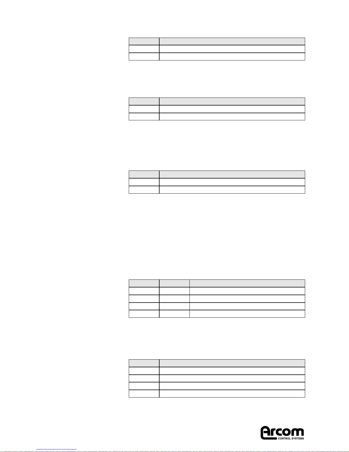
Revision History
2192-08270-000-000Revision History
J539 TARGET386EX
Page 3
PCB
V 1 Iss 2
V1 Iss 2
A
B
961107 First release.
961213 Minor edits throughout the manual.
Manual
Issue
Comments
© Copyright Arcom Control Systems Ltd. 1996
The choice of boards and systems is the responsibility of the buyer, and the use to which they are put cannot
be the liability of Arcom Control Systems Ltd. However, Arcom’s sales team is always available to assist you
in making your decision.
Page 4

J539 TARGET386EX
2192-08270-000-000 Revision History
Page 4
Page 5

Preface
The Manual
This manual details the operation and features of Arcoms
TARGET386EX boards. It has been designed as both a guide to
getting started with the TARGET386EX Development Kit and a
reference for the hardware features of the board.
Name Conventions
Throughout this document an asterisk * suffix to a signal name
denotes that a signal is active low (e.g. DATACK*).
All numbers are in decimal unless otherwise indicated. Where a
number is suffixed by h the value is in hexadecimal format.
Problem?
If you have any problems finding information about this board, or
the board fails to work, or something is missing, please contact
Arcom Customer Support at our offices in Cambridge, UK.
If the engineers are busy please leave a message, or alternatively,
send a facsimile message. Please state:
Your name, telephone and facsimile numbers
The time and date
The product name
The problem
Arcom Customer Support: Tel: 01223 412428
Fax: 01223 410457
For US callers: Tel: (816) 941 7025
For US callers: Fax: (816) 941 0343
Internet: support@arcom.co.uk
sales@arcom.co.uk
Arcom Main Switchboard: Tel: 01223 411200
Fax: 01224 403400
Contents - Packing List
In your TARGET386EX Development Kit package you should have:
A TARGET386EX in a sealed anti-static bag.
A document titled TARGET386EX User Manual (this document)
An SVIF1 Development Interface Module
A CAB-SVIF1 Development Interface Cable
A high density 3 1/2 floppy disk titled TARGET386EX Monitor
Utility Disk
A document titled TARGET386EX Monitor Manual
2192-08270-000-000Preface
J539 TARGET386EX
Page 5
Page 6

A high density 3 1/2 floppy disk titled TARGET386EX Board
Software Library
A document titled TARGET386EX Board Software Library
Shortform
A high density 3 1/2 floppy disk titled TARGET386EX
SourceVIEW
A document titled TARGET386EX SourceVIEW
Intel ApBUILDER software pack
Utility Disks
Three utility disks are provided with the TARGET386EX. One
contains source and assembled code for the monitor software preinstalled on the board together with a utility to convert assembled
code into Intel Hex format to allow code download to the board via
the monitor. The second disk contains C library routines for setting
up and controlling the board, for use in applications code together
with a disk based TARGET386EX Board Software Library Manual.
The third disk contains Arcoms SourceVIEW development and
debugging environment for use with the TARGET386EX.
Anti-Static Handling
This board contains CMOS devices which could be damaged in the
event of static electricity being discharged through them. At all
times, please observe anti-static precautions when handling the
board and always unpack and install it in an anti-static working
area.
Electromagnetic Compatibility (EMC)
The TARGET386EX is classified as a component with regard to the
European Community EMC regulations and it is the users
responsibility to ensure that systems using the board are compliant
with the appropriate EMC standards.
The STEbus variants of the TARGET386EX, when used in an Arcom
CRATE3CE enclosure, are CE approved under Arcoms STEbus
Technical Construction File.
Packaging
Please ensure that should a board need to be returned to Arcom, it
is adequately packed. Use an anti-static bag for the board and use a
box not bag to physically protect the board. Retain the original
packing if possible.
J539 TARGET386EX
2192-08270-000-000 Preface
Page 6
Page 7

Section 1. Introduction
TARGET386EX is a Eurocard sized target CPU board developed
specifically for embedded applications offering the following
features:
Intel 386EX microprocessor running at 33MHz
STEbus 8-bit expansion interface
PC/104 16-bit expansion interface
256KB SRAM as standard, 512KB option available (16-bit wide
access)
512KB Flash ROM on-board as standard (16-bit wide) with
resident monitor software
16/32KB Dual Port RAM (DPR) between 386EX and STEbus (slave
mode only)
Programmable memory and I/O maps
Two 120KBaud (max.) RS232 serial communications ports
(National Semiconductor 16450 UART compatible)
Programmable watchdog timer
Flexible hardware interrupt support including STEbus interrupt
out facility
Software development/download port (SVIF1 port)
Two user links
Two user LEDs and +5V power LED
JTAG port supporting Flash ROM programming
The TARGET386EX is available as four variants:
This manual covers all four variants and indicates where a feature
does not apply to the Single Board Computer (SBC) variants.
The TARGET386EX is shipped with a software monitor blown into
the on-board Flash ROM to allow simple exercising of the board and
downloading of application code. The remote target portion of
Arcoms SourceVIEW development software is also blown into the
Flash ROM. By using the board with the TARGET386EX
Development Kit the user can develop and debug application
software very quickly.
2192-08270-000-000Section 1. Introduction
J539 TARGET386EX
Page 7
Variant Name
TARGET386EX
TARGET386EX-H
TARGET386EX-SBC
TARGET386EX-SBC-H
STEbus Master/Slave and PC/104 Master
256k SRAM
STEbus Master/Slave and PC/104 Master
512k SRAM
STEbus Master Single Board Computer
256k SRAM
STEbus Master Single Board Computer
512k SRAM
Specification
Page 8

J539 TARGET386EX
2192-08270-000-000 Section 1. Introduction
Page 8
Page 9

Section 2. Getting Started
This section is designed to familiarise the user with the features of
the TARGET386EX and demonstrate the use of the monitor
software.
Equipment required
For STEbus board variants (PL1 fitted)
TARGET386EX SBC Development Kit
STEbus rack and backplane with power supply
IBM PC/AT compatible computer running terminal emulation
software
For SBC board variants (PL1 not fitted)
TARGET386EX SBC Development Kit
Power supply (+5V at 1A minimum) connected up to PL2 (see
Appendix B. Connections)
IBM PC/AT compatible computer running terminal emulation
software
Installation & Monitor Startup
Refer to Target386EX Quickstart Manual for more comprehensive
instructions with drawings.
1.
Ensure that the links on the TARGET386EX board are in their
default configurations (see Section 3. Links and Options).
2.
From the TARGET386EX Development Kit take the CAB-SVIF1
cable and plug the 10 pin ribbon cable connector into the SVIF1 PL2
header.
3.
Plug PL1 of the SVIF1 into PL3 (software development/download
port) on the TARGET386EX. The body of the SVIF1 should lie over
the TARGET386EX.
4.
Ensure that Link 19 is fitted so monitor EPROM is activated
5.
For STEbus variants slide the TARGET386EX into the STEbus rack
until it mates with one of the backplane connectors.
OR
For SBC variants wire the +5V power supply cable to pin 2 of the
PL2 screw terminal block and the 0V cable to either pin 5 or pin 6 of
the terminal block.
6.
Plug the 9 pin D-type connector marked channel B on the CABSVIF1 cable into one of the COM ports on the PC/AT computer.
7.
Configure the terminal emulation software on the PC/AT for
communications via the same COM port as used in No. 6 above at 19200
Baud with 8 data bits, no parity and 1 stop bit. Set the protocol to 'none'.
2192-08270-000-000Section 2. Getting Started
J539 TARGET386EX
Page 9
Page 10

8.
Turn on the STEbus rack or SBC power supply - the surface mount
power indicator LED on the TARGET386EX will illuminate.
9.
The terminal emulator will display the following (software version
may vary):
--==<< TARGMON TARGET MINI-MONITOR >>==-Version 1.03
Copyright (C) Arcom Control Systems 1996
0100>
The monitor software is now running and can be used to exercise
many areas of the board. The monitor also supports code download
from a terminal emulator and Flash ROM programming. Press the
H key to display a command list. A full manual for operating the
monitor is shipped with the TARGET386EX. Section 4. Using the
TARGET386EX describes the operation of the board in more detail
and describes the tools available to develop applications code to run
on the board.
J539 TARGET386EX
2192-08270-000-000 Section 2. Getting Started
Page 10
Page 11

Section 3. Links and Options
IMPORTANT NOTE:
STEbus variants of the TARGET386EX board are shipped in, and
power-up in, STEbus slave mode. This means that it cannot yet
access other STEbus peripheral boards. To access STEbus peripheral
boards via the monitor, links LK2 and LK3 should be fitted to drive
STEbus SYSRST* and SYSCLK* signals and General Control Register
1 (default I/O location FC06h) should be written with 07h. This sets
the board up as a default STEbus master with any memory or I/O
accesses not allocated to on-board memory or peripherals being
routed to the STEbus. See following sections and appendices for
more details of board set-up.
Default Link Positions
Note: A + next to a link position indicates the default shipping position.
LK1. STEbus timeout to TFRERR* [STEbus VARIANTS ONLY]
If an STEbus transfer initiated by the TARGET386EX is not
completed within a set time (see LK8) then a bus timeout will occur
to terminate the cycle. This may be used to generate an interrupt
(see LK15) and LK1 allows a timeout to assert the STEbus TFRERR*
signal to notify other boards in the system that there has been a
transfer problem. DO NOT FIT THIS LINK if there is an Arcom
SCIMX or SCIM386SXplus board in the system as these boards have
TFRERR* linked directly to their processor NMI line.
2192-08270-000-000Section 3. Links and Options
J539 TARGET386EX
Page 11
A B
LK18
LK16
LK12
LK13
LK11
LK7
LK19
LK17
LK15
LK14
LK10
A
B
C
D
E
F
LK5
LK6
LK4
A
B
C
D
LK1
A
LK2
B
LK3
LK8
A
B
Page 12
2192-08270-000-000
LK2. STEbus SYSRST* [NOT SBC VARIANTS]
Note: Only one board in an STEbus system should drive SYSRST*
LK3. STEbus SYSCLK [NOT SBC VARIANTS]
Note: Only one board in an STEbus system should drive SYSCLK to the
STEbus backplane. This does not have to be the STEbus default master
board.
LK4 and LK5. STEbus Dual Port RAM (DPR) size links [NOT SBC
VARIANTS]
Note: DPR can only be accessed from the STEbus when the
TARGET386EX is in STEbus slave mode (see General Control Register 1).
These links define the size of the DPR for both on-board accesses and
STEbus accesses. In STEbus default or potential master mode, when the
DPR is not accessible from the STEbus, these links must still be set to define
the size of the DPR device for on-board accesses. See LK7 for DPR STEbus
base address selection
LK6. STEbus interrupt-out [NOT SBC VARIANTS]
See General Control Register 0 and Interrupt Assignments for
details.
J539 TARGET386EX
Section 3. Links and Options
Page 12
LK4 LK5 Function
Not valid configuration
32KB DPR
16KB DPR
Not valid configuration
Omit Omit
+Omit
Fit
Fit Fit
Omit
+Fit
LK6 Function
Interrupt-out asserts STEbus ATNRQ0*
Interrupt-out asserts STEbus ATNRQ1*
Interrupt-out asserts STEbus ATNRQ2*
Interrupt-out asserts STEbus ATNRQ3*
A
B
C
D
LK1 Function
Bus timeout does not assert TFRERR*
Bus timeout asserts TFRERR*
+Omit
Fit
LK2 Function
Board receives SYSRST* from backplane
Board drives SYSRST* to backplane
+A
B
LK3 Function
Board does not drive SYSCLK to STEbus backplane
Board drives SYSCLK to STEbus backplane
+Omit
Fit
Page 13
LK7. STEbus DPR base address [NOT SBC VARIANTS]
Each position of LK7 corresponds to an STEbus address line. Fitting
a link will decode the address line logic low and omitting a link will
decode it logic high. LK7 has no effect if the board is in STEbus
default or potential master mode. See LK4 and LK5 for DPR size
selection. Default base address is D0000h with 32KB size selected.
LK8. STEbus timeout [NOT SBC VARIANTS]
LK9. Does not exist
LK10. INT0 interrupt source selection
LK11. INT1 interrupt source selection
LK12. INT2 interrupt source selection
LK13. INT3 interrupt source selection
2192-08270-000-000Section 3. Links and Options
J539 TARGET386EX
Page 13
LK7 Function
Decode STEbus A19
Decode STEbus A18
Decode STEbus A17
Decode STEbus A16
Decode STEbus A15
Decode STEbus A14 (for 32KB DPR size OMIT THIS LINK)
F
E
+D
C
+B
A
LK8 Function
4us bus timeout
8us bus timeout
A
+B
LK10 Function
STEbus ATNRQ0* [NOT SBC VARIANTS]
PC/104 IRQ10
A
+B
LK11 Function
STEbus ATNRQ1* [NOT SBC VARIANTS]
PC/104 IRQ11
A
+B
LK12 Function
STEbus ATNRQ2* [NOT SBC VARIANTS]
PC/104 IRQ12
A
+B
LK13 Function
STEbus ATNRQ3* [NOT SBC VARIANTS]
PC/104 IRQ14
A
+B
Page 14
LK14. INT6 interrupt source selection
LK15. INT7 interrupt source selection
LK16. Watchdog reset enable
LK17. User link - CPU port P1 bit 6
LK18. User link - CPU port P1 bit 7
LK19. Run mode select
Selects whether the processor runs the monitor software or the users
application code after a power-on or reset. Application code must be
set to start running at 80000H (lowest Flash ROM memory address).
Once running, code may dynamically change the mapped size of the
Flash ROM (by re-programming 386EX chip select UCS) to free more
memory space for expansion bus memory mapped peripherals.
LK20. Battery back-up from PL2
FACTORY FIT LINK - default position depends on board variant
J539 TARGET386EX
2192-08270-000-000 Section 3. Links and Options
Page 14
LK18 Function
CPU port P1 bit 6 reads as 1
CPU port P1 bit 6 reads as 0
Omit
+Fit
LK19 Function
Run application starting at memory address 80000H
Run monitor software
Omit
+Fit
LK20 Function
STEbus variant - VSTBY from PL1
SBC variant - VSTBY from PL2 pin 1
Omit
Fit
LK14 Function
DPR mailbox interrupt [NOT SBC VARIANTS]
PC/104 IRQ6
A
+B
LK16 Function
Watchdog reset disabled
Watchdog timeout generates CPU reset
A
+B
LK17 Function
CPU port P1 bit 7 reads as 1
CPU port P1 bit 7 reads as 0
Omit
+Fit
LK15 Function
STEbus TFRERR*/bus timeout interrupt [NOT SBC VARIANTS]
PC/104 IRQ15
A
+B
Page 15

LK21. ISP daisy-chain link
FACTORY FIT LINK - default position depends on board variant
This link is fitted on the SBC variant where IC10 is not fitted to allow
in-system programming of IC11 during factory test.
LK22. Processor speed
FACTORY FIT LINK
LK23 and LK24. IC21 Intel Flash compatibility
FACTORY FIT LINKS
LK23 and LK24 should be fitted if an Intel 28F400 Flash device is
fitted to the board. The default device is a Fujitsu 29F400TA.
2192-08270-000-000Section 3. Links and Options
J539 TARGET386EX
Page 15
LK21 Function
STEbus variant
SBC variant
Omit
+Fit
LK22 Function
CPU runs at 33MHz
CPU runs at 25MHz
+Omit
Fit
LK23 LK24 Function
Fujitsu device fitted
Intel device fitted
+Omit +Omit
Fit Fit
User Configuration Record
A B
LK18
LK16
LK12
LK13
LK11
LK7
LK19
LK17
LK15
LK14
LK10
A
B
C
D
E
F
LK5
LK6
LK4
A
B
C
D
LK1
A
LK2
B
LK3
LK8
A
B
Page 16

2192-08270-000-000
J539 TARGET386EX
Section 3. Links and Options
Page 16
Page 17

Section 4. Using the TARGET386EX
Programmable Memory and I/O Map
The TARGET386EX has a very flexible scheme for locating its onboard memory, peripherals and expansion busses in its memory and
I/O maps. The 386EX processor has eight outputs called
programmable chip selects, namely UCS and CS0 to CS6. These
outputs may be programmed so that they become active over a
range of memory or I/O addresses and can be used to activate
devices connected to the 386EX. The table below shows how the chip
selects are used on the TARGET386EX with the default address
ranges programmed by the monitor after initialisation.
Chip selects CS0, CS1, CS2 and UCS are activated for the address
ranges indicated in the table to control CPU accesses to the on-board
memory and peripherals.
Any CPU access to an address that is not covered by one of CS0,
CS1, CS2 or UCS is automatically directed to the default expansion
bus. On power-up or reset the default expansion bus is the PC/104
interface. STEbus board variants can access peripheral boards on
both PC/104 and STEbus. On power-up or reset the STEbus is the
non-default expansion bus. As shown in the table above, 386EX chip
selects CS3, CS4, CS5 and CS6 can be used to direct CPU accesses
that would normally go to the default expansion bus to access the
non-default expansion bus instead.
This example illustrates the use of CS3 to CS6. The monitor software
sets the TARGET386EX up so that the memory area from 48000h to
7FFFFh is directed to the PC/104 bus by default. The user has an
STEbus memory board that exists in the memory address range
60000h to 6FFFFh. Any one of CS3 to CS6 may be programmed to
cover 60000h to 6FFFFh and CPU accesses to any address in this
range will then be diverted to the STEbus instead of the PC/104.
2192-08270-000-000Section 4. Using the TARGET386EX
J539 TARGET386EX
Page 17
386EX
Chip Select
UCS
CS6
CS5
CS4
CS3
CS2
CS1
CS0
CS0
TARGET386EX Chip Select Use
Flash ROM
Accesses non-default expansion bus
Accesses non-default expansion bus
Accesses non-default expansion bus
Accesses non-default expansion bus
SVIF1 port, STEbus interrupt control
Register, General Control Registers 0
and 1
Dual port RAM (32KB)
NOT FITTED ON SBC VARIANTS
Main RAM (256KB)
Main RAM (512K)
Default Address Range
not programmed or enabled
not programmed or enabled
not programmed or enabled
not programmed or enabled
not programmed or enabled
FC00h-FFFFh, I/O
40000h - 47FFFh, MEMORY
not enabled if 512K main RAM
0 - 3FFFFh, MEMORY
0 - 7FFFF, MEMORY
Page 18

2192-08270-000-000
Note: If 512K of RAM is enabled, then there can be no access to the
PC/104 or SETbus, as there is no room for this in the memory map,
as follows.
CS3, CS4, CS5 and CS6 can be programmed very flexibly to create
multiple holes in the default bus memory or I/O space that are
directed to the non-default bus.
The default expansion bus can be changed by writing to bit 2 of
General Control Register 1. If this bit is set to 1 then the STEbus
becomes the default expansion bus. CPU accesses not covered by
CS0, CS1, CS2 or UCS will then be automatically diverted to STEbus.
CPU accesses can then be diverted to the PC/104 bus by
programming CS3 to CS6 for the appropriate address ranges.
The Board Software Library supplied with the Development Kit
fully supports programming all the 386EX chip selects.
Note: On SBC board variants PC/104 is the only available expansion bus.
Programming the chip selects that control accesses to on-board Flash
ROM, memory and I/O can also be used to move these on-board
peripherals around in the address map, see Appendix B. Reference
for more details.
Memory Map
J539 TARGET386EX
Section 4. Using the TARGET386EX
Page 18
16KB Monitor after reset
(UCS)
Top of PC/104 memory space
16KB Monitor (UCS) after initialisation
PC/104 (default)
STEbus (CS3-6)
32KB Dual Port SRAM (CS1)
256KB SRAM (CS0)
Max. Flash ROM (UCS)
3FFFFFFh
3FFC00h
1000000h
100000h
FFFFFh
FC000h
FBFFFh
80000h
7FFFFh
48000h
40000h
3FFFFh
00000h
ROM
RAM
or 512K
RAM
1M
512K
0
The address range if the ROM or RAM can
be changed to make a hole in the memory
map for access to the external busses.
Page 19

Memory Map After Power-up/Reset
After reset the upper chip select UCS is enabled with the entire
64MB memory address space as its address block. This allows the
boot monitor program to run from the top of memory. By default
the monitor program will run in real mode, the UCS register is then
programmed by the monitor software to assert the Flash ROM chip
select at addresses from 80000h to FFFFFh (512KB).
The state of LK19 tells the monitor whether to run itself or the users
application code. Application code must always start running from
address 80000h (bottom of Flash ROM). Having the Flash ROM
occupy this much of the memory map may obscure areas of the
memory map required by PC/104 or STEbus peripheral boards. If
this is the case then the application code can be written to reprogram the start address of UCS, while it is running to effectively
limit the size of the Flash ROM. Code should be written to jump into
the reduced Flash ROM area and then to re-program UCS for the
new size.
Memory space between the bottom of ROM and the top of main
RAM (location selected by CS0) will be automatically mapped to the
default expansion bus (STEbus or PC/104 depending on bit 2 of
General Control Register 1). CS3-6 can be programmed to direct
accesses to the non-default bus. CS1 decodes the on-board address
of the 16/32KB Dual Port RAM, this is fully re-locatable.
Note: when running the monitor software on 512KB RAM variants
of board the extra 256KB of RAM is not accessible until chip select
CS0 is re-programmed because in order to gain access to STEbus or
PC/104 bus or the on-board DPR located by CS1, either the bottom
of the Flash ROM area must be moved up the memory map by
programming UCS or the top of the on-board main RAM must be
moved down by programming CS0.
2192-08270-000-000Section 4. Using the TARGET386EX
J539 TARGET386EX
Page 19
Page 20

I/O Map
I/O Map After Power-up/Reset
The 386EX I/O has 64KB of I/O space. This is routed to the default
bus (STEbus or PC/104) except for the following locations. I/O
locations 22h and 23h are reserved for the I/O map configuration
register REMAPCFG. This register can change the way the I/O
space is set up for the 386EX. The monitor program sets the 386EX
up into Expanded Mode by default. This allows all the on-chip
peripherals to be mapped to address between F000h and F8FFh.
Programmable chip select line CS2 is used to select on-board
peripherals (STEbus interrupt control, interrupt out and bus timeout
interrupt clear, SVIF1 port). As CS2 can be programmed to be
anywhere in the I/O space (or, indeed, the memory space) the
location of this on-board peripheral control register block may be
relocated to any convenient location. In order to allow the maximum
space for I/O expansion on STEbus or PC/104 the monitor program
sets this register block location up to start at FC00h.
PC/104 is the only expansion bus available on SBC variants.
J539 TARGET386EX
2192-08270-000-000 Section 4. Using the TARGET386EX
Page 20
PC/104 (default)
STEbus (CS3-6)
SVIF1 Port
General Control Register 1 (repeat)
General Control Register 1
General Control Register 0 (repeat)
General Control Register 0
STEbus Control Register (repeat)
STEbus Control Register
PC/104 (default)
STEbus (CS3-6)
On-chip peripherals (Interrupt controllers, timers, UARTS)
PC/104 (default)
STEbus (CS3-6)
386EX 16bit REMAPCFG
register (not movable)
STEbus or PC/104
FFFFh
FC0Fh
FC0Ch
FC07h
FC06h
FC05h
FC04h
FC01h
FC00h
F8FFh
F000h
EFFFh
0023h
0022h
0000h
Page 21

On-Board Control Registers
SVIF1 Port Registers
The SVIF1 port takes up 4 bytes of I/O space.
The default base address of the SVIF1 port under the monitor
software is I/O FC0Ch.
STEbus Interrupt Control Register [NOT SBC VARIANTS]
This register controls the NOR gates that pass the STEbus ATNRQx*
signals to 386EX INT0-3 inputs.
The default address of this register under the monitor software is
I/O FC00h. It is repeated at FC01h.
Signal description:
General Control Register 0 [NOT SBC VARIANTS]
This register is used to generate interrupts out onto the STEbus with
the board in STEbus slave mode and clear the STEbus DPR mailbox
interrupt.
The default address of this register under the monitor is I/O FC04h.
It is repeated at FC05h.
Signal description:
2192-08270-000-000Section 4. Using the TARGET386EX
J539 TARGET386EX
Page 21
A1
1 1
0
1
0
Channel A Data
Channel B Data
Channel A Control
Channel B Control
1
0
0
A0 Function
Bit 7
Unused bits
6 5 4 3
S_INT32S_INT21S_INT10S_INT0
Bit 7
Unused bits
6 5 4 3
Unused2INTOUT1BTOCLR0MBXCLR
Signal
S_INT3
S_INT2
S_INT1
S_INT0
Reset State
0
0
0
0
R/W
R/W
R/W
R/W
R/W
Description
Enables (0) and disables (1) ATNRQ3* (see
interrupts through to INT3. Set/reset by interrupt
service routine.
Enables (0) and disables (1) ATNRQ2*. See S_INT3
Enables (0) and disables (1) ATNRQ1*. See S_INT3
Enables (0) and disables (1) ATNRQ0*. See S_INT3
Signal
INTOUT
BTOCLR
S_INT1
Reset State
0
0
0
R/W
W
W
W
Description
Writing 1 to this bit generates an interrupt out
onto the STEbus in slave mode. This bit is reset by
an STEbus access to the DPR mailbox area.
Writing 1 clears the STEbus bus timeout/TFRERR interrupt
Writing 1 to this bit clears the STEbus DPR mailbox interrupt
Page 22

General Control Register 1 [NOT SBC VARIANTS]
This register is used to define the default expansion bus (STEbus or
PC/104), the function of the STEbus arbiter and whether the board
is STEbus default master, potential master or slave.
The default address of this register under the monitor software is
I/O FC06h. It is repeated at FC07h.
Signal Description
The SARB1 and SARB0 signals have the following function:
User Links and LEDS
The TARGET386EX has two user links and two user LEDs and a link
that determines whether the monitor software or application code is
run on power-up or reset. These links and LEDs are connected
directly to the 386EX processors integral parallel port pins as
follows:
Links
J539 TARGET386EX
2192-08270-000-000 Section 4. Using the TARGET386EX
Page 22
Reference
LK17
LK18
LK19
386EX Parallel Port Connection
Port P1 bit 6
Port P1 bit 7
Port P3 bit 6
(this link is used for run mode selection by the monitor)
Bit 7
Unused bits
6 5 4 3
INTCO
M2DEFSTE1SARB10SARB0
Signal
INTCOM
DEFSTE
SARB1
SARB0
Reset State
0
0
0
0
R/W
R/W
R/W
R/W
R/W
Description
Interrupt compatibility . If set /EN3-0 (see
interrupt Assignments) are permanently low.
Off-board cycles routed to PC/104 (0) or STEbus (1)
STEbus arbiter and bus requester control.
STEbus arbiter and bus requester control.
SARB1 SARB0 Function
0
0
1
1
0
1
0
1
STEbus slave. STEbus arbiter disabled, DPR,
mailbox and interrupt out enabled.
STEbus potential master on BUSRQ0*. STEbus
arbiter disabled , DPR and mailbox disabled and
interrupt out enabled.
STEbus potential master on BUSRQ1*. STEbus
arbiter disabled , DPR and mailbox disabled and
interrupt out enabled.
STEbus default master. STEbus arbiter enabled. DPR
and mailbox disabled and interrupt out enabled.
Page 23

LEDs
The C library routines supplied with the TARGET386EX fully
support the configuration of and access to these peripherals. Intels
ApBUILDER software, also supplied with the board, allow the user
to set up and access the ports at a lower software level.
Interrupt Assignments
Interrupts from STEbus, PC/104 and on-board peripherals are
routed to the 386EX INT7-0 lines via links for ease of configuration.
The link arrangement is shown below.
STEbus interrupts are level triggered, 386EX on-board peripherals
use edge triggered interrupts. The NOR gates shown in the
interrupt connection diagram shown above allow true level
triggered interrupts to be used on the STEbus. This is best illustrated
with an example. An STEbus board asserts ATNRQ2* low which
generates a low-high transition on interrupt to the CPU on INT2.
The software interrupt handler must know which ATNRQ* line was
asserted. On entering the interrupt handler the software writes a 1 to
bit 2 of the STEbus Control Register to disable the NOR gate
associated with ATNRQ2*. This causes the INT line to go low. The
interrupt handler then acts to clear the source of ATNRQ2*. At the
end of the interrupt handler the software writes a 0 to bit 2 of the
STEbus Control Register 0 and re-enables the NOR gate. If there was
only one source of ATNRQ2* then the INT2 line stays low and no
further interrupt is generated. If there are multiple sources of
ATNRQ2* and the line remains low after one source has been
2192-08270-000-000Section 4. Using the TARGET386EX
J539 TARGET386EX
Page 23
Reference
D2 (RED)
D£ (GREEN)
386EX Parallel Port Connection
Port P3 bit 1
Port P3 bit 0
ATNRQ0*
ATNRQ1*
ATNRQ2*
ATNRQ3*
/EN0
/EN1
/EN2
/EN3
PC_IRQ10
PC_IRQ11
PC_IRQ12
PC_IRQ14
INT0
INT1
INT2
INT3
INT4
INT6
INT7
INT5
PC_IRQ5
PC_IRQ7
PC_IRQ6
PC_IRQ15
MAILBOX_INT
TFRERR_IN/BTO
INT_OUT
ATNRQ3*
ATNRQ2*
ATNRQ1*
ATNRQ0*
A
B
A
B
A
B
A
B
A
B
A
B
A
D
LK10
LK11
LK12
LK13
LK14
LK15
LK6
Page 24

cleared then re-enabling the NOR gate causes another low-high
transition on the INT2 line and another interrupt is generated. The
interrupt handler is then called again and the process is repeated
until there are no further interrupts on ATNRQ2*. Thus multiple
interrupt sources can share an ATNRQ* level.
The STEbus variant of the board is capable of generating an
interrupt out onto the STEbus in all its STEbus operating modes by
writing 1 to General Control Register 0 bit 2. The ATNRQ* level that
is asserted is set up on link LK6. If the board is in STEbus slave mode
then this interrupt out is cleared by a write access to the mailbox
area of DPR from an STEbus master.
Note that the STEbus board variants can only drive or receive
interrupts on STEbus ATNRQ0*, ATNRQ1*, ATNRQ2* or
ATNRQ3*. ATNRQ4-7* are not connected to the board.
The diagram over the page shows how the INTx pins of the 386EX
processor relate to the interrupt request (IR) numbers used by the
interrupt controller.
J539 TARGET386EX
2192-08270-000-000 Section 4. Using the TARGET386EX
Page 24
Interrupt Control Unit
Page 25

STEbus Support [NOT SBC VARIANTS]
The TARGET386EX is compliant with the STEbus IEEE1000
specification. General Control Register 1 bits 0 and 1 define whether
the board is an STEbus default master, potential master or slave. It
can perform memory and I/O reads and writes as a default master
or potential master requesting the bus on BUSRQ0* or BUSRQ1*. As
an STEbus slave the board appears as a 16KB or 32KB (see LK4 and
LK5) window in the STEbus 1MB memory space at a base address
set by LK7. The top 4KB block of the DPR window is designated as
a mailbox area. Any writes to this area will generate a mailbox
interrupt to the CPU on board (if enabled by LK14 position A). Write
accesses to the mailbox area also clear the interrupt out from the
board if it is asserted. The on-board base address of the DPR area as
seen by the CPU is defined by chip select CS1 (see Memory Map).
PC/104 Support
The TARGET386EX is compliant with version 2.3 of the PC/104
specification. It supports memory and I/O reads and writes to as a
sole master to 8 and 16 bit PC/104 peripheral boards. It does not
support DMA or other PC/104 masters in the same module stack.
Battery Back-up
The TARGET386EX supports battery backup of its main system
SRAM via the +VSTBY line on the STEbus or via pin 1 of the power
connector PL2 on the SBC variant.
On STEbus variants a +5V source should be connected between
+VSTBY (+ve terminal) and GND (-ve terminal) on the STEbus
backplane.
On SBC variants a +5V source should be connected between pin 1
(+ve terminal) and pin 6 (-ve terminal) of PL2.
Battery backup current is approximately 140uA.
Utility Files
The TARGET386EX Utility consists of three files:
The source and assembled code for the monitor software and a
utility called BIN2HEX which converts the binary files to Intel Hex
format to enable them to be downloaded using the on-board
monitor. The operating manual for the monitor software is shipped
with the board.
The Next Step
The monitor software installed allows the user to become familiar
with the boards basic features. Arcom supplies a number of options
to aid the user in developing application code to fully utilise the
TARGET386EXs facilities.
2192-08270-000-000Section 4. Using the TARGET386EX
J539 TARGET386EX
Page 25
Page 26

2192-08270-000-000
J539 TARGET386EX
Section 4. Using the TARGET386EX
Page 26
A board utility library written in C is supplied with the
Development Kit. This contains routines that allow application code
to easily set up and control on-board peripherals such as the
interrupt controller, CPU programmable chip selects, serial
communications channels, watchdog timer, counter/timers, user
links and LEDs and control register support. For users who wish to
develop their own routines, Appendix D. Bibliography lists the
datasheets for the on-board peripherals.
A copy of Intels ApBUILDER software is supplied with the
Development Kit. This allows the user to configure the 386EX onchip peripherals and generate code blocks in assembler or C to set
them up.
SourceVIEW, a solution to code development and debugging for
the TARGET386EX is shipped with the TARGET386EX
Development Kit. The board is shipped with the remote target
portion of the system blown in the Flash ROM at board address
80000H. This runs if LK19 jumper is removed before poweron/reset. With the host portion of the SourceVIEW system running
on a PC/AT compatible, a complete source level debugging
environment can quickly be constructed.
Arcom can supply a range of other tools for source level
development and debugging as well as real time operating systems
and development tools. Please contact Arcom for details.
For users who do not wish to download code to the board via the
SVIF port Arcom can supply a programming kit which allows the
Flash ROM to be programmed directly via PL7, the JTAG port.
Using the TAPFLASH utility and cable, which plugs into a PC/AT
parallel port, any area of the Flash ROM, including the monitor code
section, may be programmed with the users application code. Please
contact Arcom for more details of the TAPFLASH product.
Page 27

Section 5. Troubleshooting
2192-08270-000-000Section 5. Troubleshooting
J539 TARGET386EX
Page 27
Problem Suggestions
No monitor signon message on
terminal when
running with SVIF1
Cant access dual
port RAM from
STEbus
Cant access
STEbus peripheral
board
Cant access PC/104
peripheral board
Check connections to correct COM port
Check links in default positions especially LK19
(should be fitted)
Check baud rate, stop bits and parity of terminal
Check power on board - red surface mount LED
should be lit
Check base address and DPR size selection on
LK7, LK4 and LK5
Check board is in STEbus slave mode (General
control register 1)
Check no other boards in system use same
STEbus Memory window as DPR
Check TARGET386EX is not in reset state
Check board is in default or potential master
mode. If in potential master mode check that
there is an STEbus default master in the system
to do the bus arbitration
Check that SYSRST* is being driven on power-
up by one board only in the system
Check that SYSCLK* is being driven by only one
board in the system
Check that STEbus address range being accessed
is available off-board (is it covered by one of the
on-board memory or peripheral chip selects)
• Is the STEbus the default bus (see General
Control Register 1), if not check that at least one
of chip selects CS3-6 been set up to cover the
required address range
• Is the address range being accessed available to
the PC/104 bus - is it covered by one of the onboard peripheral chip selects
• Is PC/104 the default expansion bus (see General
Control Register 0), if not check that at least one
of the chip selects CS3-6 has been set up to cover
the required address range
Is the PC/104 board correctly plugged on to
the board
Page 28

2192-08270-000-000
J539 TARGET386EX
Section 5. Troubleshooting
Page 28
Page 29

Appendix A. Specification
Microprocessor
Intel 80386EX (C-step silicon)
Speed
33MHz
Memory
512KB Flash ROM (16 bits wide, two wait states) top 16KB occupied
by monitor software
256KB or 512KB main system SRAM (16 bits wide, one wait state)
32KB of SRAM dual ported with STEbus (8 bits wide)
Peripherals
2 x 16450 UART compatible RS232 serial communications ports
(120KBaud max.) with RX, TX, CTS, RTS, DSR, DTR, DCD and RI
Arcom SVIF debug/development port
Watchdog timer programmable from 0 to 130s in 30ns intervals can
generate interrupts and link selectable CPU reset
3 Intel 8254 compatible counter/timers max counter interval 1s.
Each counter can generate an interrupt
Two user LEDs
Two user links plus run monitor/run application link
Power monitor generates CPU reset if +5V supply drops below
4.62V +/- 0.12V.
Reset button connector
Expansion
STEbus IEEE1000 compatible default master and bus arbiter,
potential master and slave modes PC/104 version 2.3 compatible, 16
and 8 bit. DMA and MASTER* modes not supported
Temperature
Operating: 0 to 55
°C
Storage: 0 to 70°C
Humidity
10% to 80% RH (non-condensing)
Power
+5V @ 600mA typical
+12V and -12V routed to PL1, PL2 and PL6 but not used on board
Battery
External +5V @ 140uA
Dimensions
160mm x 100mm
Weight
145g (TARGET386EX)
MTBF
224200 hours
2192-08270-000-000Appendix A. Specification
J539 TARGET386EX
Page 29
Page 30

2192-08270-000-000
J539 TARGET386EX
Appendix A. Specification
Page 30
Page 31

Appendix B. Connections
PL1. STEbus Connector
Standard 64way a&c row DIN41612 right angle PCB mount plug.
Pin-out in accordance with IEEE1000 specification.
PL2. External Power Connector
Phoenix MCV series two part combicon screw terminal connector.
Pinout as:
PL3. SVIF1 Development Interface Module Connector
20 way header with pinout as:
PL4. ispLSI Programming Connector - DO NOT USE
2mm grid 10-way connector with pinout as:
2192-08270-000-000Appendix B. Connections
J539 TARGET386EX
Page 31
nc/VSTBY
+5V
+12V
-12V
GND
GND
1
2
3
4
5
6
GND
/RD
D0
D2
D4
D6
A0
/CS
nc
+5V
1 2
3 4
5 6
7 8
9 10
11 12
13 14
15 16
17 18
19 20
GND
/WR
D1
D3
D5
D7
A1
/SVINT
CLK
+5V
GND
/ISPEN
ISPSDI
nc
+5V
1 2
3 4
5 6
7 8
9 10
ISPSDO
ISPMODE
ISPSCK
nc
GND
PL1
Page 32

PL5 and PL6. PC/104 Connectors
One 40 way and one 64 way non-stackthrough 0.1 grid socket
connectors. Pinout and physical arrangement in accordance with
PC/104 specification version 2.3.
PL7. JTAG Port
6 pin Dubox header
J539 TARGET386EX
2192-08270-000-000 Appendix B. Connections
Page 32
GND
MEMCS16*
IOCS16*
IRQ10
IRQ11
IRQ12
IRQ15
IRQ14
pull-up
nc
pull-up
nc
pull-up
nc
pull-up
nc
+5V
nc
GND
GND
D1 C1
D2 C2
D3 C3
D4 C4
D5 C5
D6 C6
D7 C7
D8 C8
D9 C9
D10 C10
D11 C11
D12 C12
D13 C13
D14 C14
D15 C15
D16 C16
D17 C17
D18 C18
D19 C19
D20 C20
GND
SBHE*
A23
A22
A21
A20
A19
A18
A17
MEMRD*
MEMWR*
D8
D9
D10
D11
D12
D13
D14
D15
nc
nc
D7
D6
D5
D4
D3
D2
D1
D0
IOCHRDY
AEN (GND)
A19
A18
A17
A16
A15
A14
A13
A12
A11
A10
A9
A8
A7
A6
A5
A4
A3
A2
A1
A0
GND
A1 B1
A2 B2
A3 B3
A4 B4
A5 B5
A6 B6
A7 B7
A8 B8
A9 B9
A10 B10
A11 B11
A12 B12
A13 B13
A14 B14
A15 B15
A16 B16
A17 B17
A18 B18
A19 B19
A20 B20
A21 B21
A22 B22
A23 B23
A24 B24
A25 B25
A26 B26
A27 B27
A28 B28
A29 B29
A30 B30
A31 B31
A32 B32
GND
RESET
+5
nc
nc
nc
-12
ENDXFR*
+12
nc
SMEMW*
SMEMR*
IOW*
IOR*
pull-up
nc
pull-up
nc
pull-up
SYSCLK
IRQ7
IRQ6
IRQ5
nc
nc
pull-up
nc
BALE
+5
OSC
GND
GND
TDO
TDI
TMS
TCK
+5
GND
1
2
3
4
5
6
PL5 PL6
Page 33

PL8 and PL9. RS232 Serial Port connectors
Two 9-way D-type plugs. Pinout as:
PL10. Push-button Reset
2 pin Dubox header.
SVIF1 Development Interface Module , PL2
10 way IDC ribbon cable header for use with CAB-SVIF1 in
development system
2192-08270-000-000Appendix B. Connections
J539 TARGET386EX
Page 33
GND
RST_IN
1
2
Channel A TX
Channel A RTS
GND
Channel B CTS
Channel B RX
1 2
3 4
5 6
7 8
9 10
Channel A RX
Channel A CTS
GND
Channel B RTS
Channel B TX
5
4
3
2
1
9
8
7
6
DCD
RXD
TXD
DTR
GND
DSR
RTS
CTS
RI
Page 34

2192-08270-000-000
J539 TARGET386EX
Appendix B. Connections
Page 34
Page 35

Appendix C. Reference
The STEbus and the TARGET386EX
STEbus is a high reliability 8 bit backplane system, ideal for
industrial I/O applications with powerful facilities for multiprocessing and interrupt handling.
STEbus boards are classified as either bus masters or slaves. A bus
master can initiate a bus transfer whereas a slave can only respond.
Generally bus masters are CPU boards which access memory and
I/O peripheral slave boards. Some slave boards do have on-board
microprocessors.
STEbus can support up to three bus masters in a system. One of
these is the default master, the other two are potential masters. The
default master contains a bus arbiter that controls which master
board has control on a transfer-by-transfer basis. Potential masters
request control of the bus from the bus master on BUSRQ0* or
BUSRQ1*. The arbiter grants bus control to one of the requesting
boards on a priority basis, BUSRQ0* has highest priority and
BUSRQ1* has lower priority, with BUSACK0* and BUSACK1*
signals respectively. Lowest priority is the default master which has
control of the bus when no other master requires it.
STEbus master and slave boards may be placed in any slot in the
STEbus backplane.
The TARGET386EX can act as either an STEbus master or slave. It
may also be used in multi-master systems. The STEbus mode is
controlled by on-board General Control Register 1. In default master
mode the board has an on-board bus arbiter enabled. Bus arbitration
is entirely transparent to any software running on any of the
masters. In bus requester mode the on-board arbiter is disabled and
another board must contain the arbiter. In slave mode the arbiter is
disabled and the TARGET386EX can make no STEbus accesses. Bus
masters may talk to the TARGET386EX in slave mode via the dual
port RAM which is only enabled in slave mode.
Only one board in an STEbus system should drive the 16MHz
SYSCLK signal.
STEbus slaves are accessed simply by memory and I/O read and
write commands from the master processor. These generate address
strobe (ADRSTB*), data strobe (DATSTB*), command modifier
(CM2 to CM0), address and data signals to the STEbus. Slave boards
that decode their address for a transfer respond with a DATACK*
signal when they have accepted or placed data on the STEbus. Slave
boards should be configured to fit in the STEbus memory or I/O
space available on the TARGET386EX. Note that if an STEbus slave
has a non-movable address then the memory and I/O maps on the
TARGET386EX are very flexible and may be re-configured using
2192-08270-000-000Appendix C. Reference
J539 TARGET386EX
Page 35
Page 36

registers within the 386EX processor (see memory and I/O maps in
Section 4. Using the TARGET386EX).
There are eight interrupt request lines on the STEbus, ATNRQ7* to
ATNRQ0*. These are usually driven by slave boards to request
action from a master. STEbus interrupt lines are level triggered and
slave boards may share interrupt lines. The TARGET386EX
monitors ATNRQ3*, ATNRQ2*, ATNRQ1* and ATNRQ0*. The
Target386EX may also generate an interrupt on any of these four
lines to the STEbus in either default master, potential master or slave
mode.
All transfers on the STEbus are monitored by bus timeout circuit
that terminates any cycles that are longer than 8us or 4us (link
selectable). This is required because if no slave board responds to an
STEbus cycle then the bus could stay in that bus cycle indefinitely,
the bus timeout monitor prevents this. Bus timeouts on the
TARGET386EX can optionally (link) generate an interrupt to the
386EX processor to indicate that a transfer problem took place.
PC/104 and the TARGET386EX
PC/104 is a small form factor version of the PC/AT ISA bus (IEEE
P996 draft standard) designed for embedded applications. The
TARGET386EX is a PC/104 16/8 bit master controller. It allows 16
and 8 bit cycles with dynamic bus sizing (16 bit transfers to 8 bit
boards are automatically split into two 8 bit transfers) for both
memory and I/O PC/104 peripherals. The TARGET386EX PC/104
interface allows PC/104 expansion boards to extend bus transfers
using the IOCHRDY signal and to shorten the default cycle length
using ENDXFR*.
The TARGET386EX PC/104 interface supports a subset of the
PC/AT interrupts. These are edge triggered.
The TARGET386EX PC/104 interface does not support PC/104
DMA or MASTER* cycles.
There is a PC/104 bus timeout monitor that terminates bus cycles
that have been extended to greater than 16us by IOCHRDY.
STEbus and PC/104 interaction on the TARGET386EX
The TARGET386EX can direct expansion bus accesses to either the
STEbus or the PC/104 bus. At power-up the PC/104 bus is defined
as the default bus and the board is reset to be an STEbus slave. All
accesses to addresses not covered by one of the 386EX chip select
ranges (see Section 4. Using the TARGET386EX) is directed out onto
the PC/104 bus. The DEFSTE bit in on-board General Control
Register 1 changes the default expansion bus to STEbus (note that
bits 0 and 1 of this register must also be changed to configure the
board as an STEbus master before STEbus accesses can occur). Four
of the 386EX chip select lines are left free for application software to
J539 TARGET386EX
2192-08270-000-000 Appendix C. Reference
Page 36
Page 37

program (CS6 to CS3). When one or more of these chip selects is
programmed to cover a memory (or I/O) address range then an
access to a memory (or I/O) address in that range is automatically
re-directed to the non-default bus ie. STEbus if the PC/104 is the
default bus or PC/104 if STEbus is the default. Using these chip
selects then gives the user the ability to mix PC/104 boards and
STEbus boards in the address map of the TARGET386EX
transparently to the application code.
By using registers within the 386EX processor the address ranges
used for the various on-board memory and I/O peripherals can be
changed. This means that if the default on-board area of any onboard device conflicts with a device on the STEbus or the PC/104
bus then the chip select that controls that device can be reprogrammed to move the Flash ROM in the memory map. For
example, the default size of the Flash ROM is 512KB. If a PC/104
peripheral needs to exist in the address range A0000H to C7FFFH
then the start address of the Flash ROM could be re-programmed to
C8000H with the end address kept to FFFFFH. This reduces the size
of the Flash ROM available but the PC/104 device has been easily
accommodated into the TARGET386EX memory map.
Programming the 386EX chip selects is fully supported in the C
board library supplied with the board.
2192-08270-000-000Appendix C. Reference
J539 TARGET386EX
Page 37
Page 38

2192-08270-000-000
J539 TARGET386EX
Appendix C. Reference
Page 38
Page 39

Appendix D. Bibliography
Intel386EX Embedded Microprocessor Data Sheet
Intel Order No.: 272420-005
Intel386EX Embedded Microprocessor Users Manual
Intel Order No.: 272485-002
These may be ordered from these Intel literature centres:
tel: 1-800-548-4725 U.S. and Canada
tel: 708-296-9333 U.S. (from overseas)
tel: 44(0)1793-431155 Europe (U.K)
tel: 44(0)1792-421333 Germany
tel: 44(0)1793-421777 France
tel: 81(0)120-47-88-32 Japan (fax only)
IEEE Standard for an 8-bit Backplane Interface: STEbus
ANSI/IEEE 1000-1987
The Institute of Electrical and Electronic Engineers Inc.
345 East 47th Street
New York NY 10017
USA
ISBN 1-55937-002-5
PC/104 Specification, Version 2.3
PC/104 Consortium
P.O. Box 4303
Mountain View
CA 94040
USA
tel: 415-903-8304
fax: 415-967-0995
IEEE P996 Draft Standard
IEEE Standards Office
445 Hoes Lane
Piscataway
NJ 08854
USA
2192-08270-000-000Appendix D. Bibliography
J539 TARGET386EX
Page 39
Page 40

2192-08270-000-000
J539 TARGET386EX
Appendix D. Bibliography
Page 40
Page 41

Appendix E. Product Issue Changes
2192-08270-000-000Appendix E. Product Issue Changes
J539 TARGET386EX
Page 41
Page 42

2192-08270-000-000
J539 TARGET386EX
Appendix E. Product Issue Changes
Page 42
Page 43

Appendix F. Circuit Diagrams
2192-08270-000-000Appendix F. Circuit Diagrams
J539 TARGET386EX
Page 43
Page 44

2192-08270-000-000
J539 TARGET386EX
Appendix F. Circuit Diagrams
Page 44
Page 45

2192-08270-000-000Appendix F. Circuit Diagrams
J539 TARGET386EX
Page 45
Page 46

2192-08270-000-000
J539 TARGET386EX
Appendix F. Circuit Diagrams
Page 46
Page 47

2192-08270-000-000Appendix F. Circuit Diagrams
J539 TARGET386EX
Page 47
Page 48

2192-08270-000-000
J539 TARGET386EX
Appendix F. Circuit Diagrams
Page 48
Page 49

2192-08270-000-000Appendix F. Circuit Diagrams
J539 TARGET386EX
Page 49
Page 50

2192-08270-000-000
J539 TARGET386EX
Appendix F. Circuit Diagrams
Page 50
Page 51

2192-08270-000-000Appendix F. Circuit Diagrams
J539 TARGET386EX
Page 51
Page 52

2192-08270-000-000
J539 TARGET386EX
Appendix F. Circuit Diagrams
Page 52
 Loading...