


ATMEL AT27BV400-15TC, AT27BV400-15RI, AT27BV400-12JC, AT27BV400-15RC, AT27BV400-15JC Datasheet
...
Features |
|
|
|
|
|
|
|
|
|
|
|
|
|
|
|
|
|
|
|
||
• Fast Read Access Time - 120 ns |
|
|
|
|
|
|
|
|
|
|
|
|
|
|
|
|
|
||||
• Word-wide or Byte-wide Configurable |
|
|
|
|
|
|
|
|
|
|
|
|
|
|
|
|
|
||||
• Dual Voltage Range Operation |
|
|
|
|
|
|
|
|
|
|
|
|
|
|
|
|
|
||||
|
– Unregulated Battery Power Supply Range, 2.7V to 3.6V |
|
|
|
|
|
|
|
|
|
|||||||||||
|
or Standard 5V ± 10% Supply Range |
|
|
|
|
|
|
|
|
|
|
|
|
|
|
|
|
|
|||
• 4-Megabit Flash and Mask ROM Compatable |
|
|
|
|
|
|
|
|
|
|
|
|
|
|
|
|
|||||
• |
Low Power CMOS Operation |
|
|
|
|
|
|
|
|
|
|
|
|
|
|
|
|
|
|||
|
– 20 μA Maximum Standby |
|
|
|
|
|
|
|
|
|
|
|
|
|
|
|
|
|
|||
• |
– 10 mA Max. Active at 5 MHz for V CC = 3.6V |
|
|
|
|
|
|
|
|
|
|
|
|
|
4-Megabit |
|
|||||
JEDEC Standard Packages |
|
|
|
|
|
|
|
|
|
|
|
|
|
|
|
|
|||||
|
|
|
|
|
|
|
|
|
|
|
|
|
|
|
|
|
|||||
|
– 44-Lead PLCC |
|
|
|
|
|
|
|
|
|
|
|
|
|
|
|
(256K x 16 or |
|
|||
|
– 44-Lead SOIC (SOP) |
|
|
|
|
|
|
|
|
|
|
|
|
|
|
|
|
||||
|
– 48-Lead TSOP (12 mm x 20 mm) |
|
|
|
|
|
|
|
|
|
|
|
|
|
|
|
|
||||
• High Reliability CMOS Technology |
|
|
|
|
|
|
|
|
|
|
|
|
|
|
|
512K x 8) |
|
||||
|
– 2,000 ESD Protection |
|
|
|
|
|
|
|
|
|
|
|
|
|
|
|
|
||||
|
– 200 mA Latchup Immunity |
|
|
|
|
|
|
|
|
|
|
|
|
|
|
|
Unregulated |
|
|||
• |
Rapid™ |
Programming Algorithm - 50 μs/word (typical) |
|
|
|
|
|
|
|
|
|
|
|
|
|||||||
• CMOS and TTL Compatible Inputs and Outputs |
|
|
|
|
|
|
|
|
|
|
|
|
|
Battery-Voltage |
™ |
||||||
|
– JEDEC Standard for LVTTL and LVBO |
|
|
|
|
|
|
|
|
|
|
|
|
|
|
|
|||||
|
|
|
|
|
|
|
|
|
|
|
|
|
|
|
|
|
|||||
|
|
|
|
|
|
|
|
|
|
|
|
|
|
|
|
|
|
||||
• Integrated Product Identification Code |
|
|
|
|
|
|
|
|
|
|
|
|
|
|
|
High Speed |
|
||||
• Commercial and Industrial Temperature Ranges |
|
|
|
|
|
|
|
|
|
|
|
|
|
|
|||||||
|
|
|
|
|
|
|
|
|
|
|
|
|
|
|
|||||||
Description |
|
|
|
|
|
|
|
|
|
|
|
|
|
|
|
|
OTP EPROM |
|
|||
The AT27BV400 is a high performance low-power, low-voltage 4,194,304-bit one time |
|
|
|||||||||||||||||||
programmable read only memory (OTP EPROM) organized as either 256K by 16 or |
AT27BV400 |
|
|||||||||||||||||||
512K by 8 bits. It requires only one supply in the range of 2.7 to 3.6V in normal read |
|
||||||||||||||||||||
|
|
|
|
|
|
|
|
|
|
|
|
|
|
|
|
|
|
|
(continued) |
|
|
Pin Configurations |
|
|
|
|
|
PLCC |
|
|
|
|
Preliminary |
|
|||||||||
|
|
|
|
|
|
|
|
|
|
|
|||||||||||
|
|
|
|
|
|
|
|
|
|
|
|
|
|
|
|
|
|||||
|
Pin Name |
Function |
|
|
A5 |
A6 |
A7 |
A17 |
NC |
GND |
NC |
A8 |
A9 |
A10 |
A11 |
|
|
|
|
||
|
|
|
|
|
|
|
|
|
|
|
|
|
|
|
|
|
|
||||
|
A0 - A17 |
|
Addresses |
|
|
6 |
5 |
4 |
3 |
2 |
1 |
44 |
43 |
42 |
41 |
40 |
|
|
|
|
|
|
|
|
A4 |
7 |
|
|
|
|
|
|
|
|
|
39 |
A12 |
|
|
|
|||
|
|
|
|
|
|
|
|
|
|
|
|
|
|
|
|
|
|
||||
|
|
|
|
|
|
A3 |
8 |
|
|
|
|
|
|
|
|
|
38 |
A13 |
|
|
|
|
O0 - O15 |
Outputs |
|
A2 |
9 |
|
|
|
|
|
|
|
|
|
37 |
A14 |
|
|
|
||
|
|
A1 |
10 |
|
|
|
|
|
|
|
|
|
36 |
A15 |
|
|
|
||||
|
O15/A-1 |
|
Output/Address |
|
A0 |
11 |
|
|
|
|
|
|
|
|
|
35 |
A16 |
|
|
|
|
|
|
|
CE |
12 |
|
|
|
|
|
|
|
|
|
34 |
BYTE/VPP |
|
|
||||
|
|
|
Byte Mode/ |
|
GND |
13 |
|
|
|
|
|
|
|
|
|
33 |
GND |
|
|
|
|
|
BYTE/VPP |
|
OE |
14 |
|
|
|
|
|
|
|
|
|
32 |
O15/A-1 |
|
|
|
|||
|
Program Supply |
|
O8 |
16 |
|
|
|
|
|
|
|
|
|
30 |
O14 |
|
|
|
|||
|
|
|
|
|
|
O0 |
15 |
|
|
|
|
|
|
|
|
|
31 |
07 |
|
|
|
|
|
|
|
|
|
O1 |
17 |
19 |
20 |
21 |
22 |
23 |
24 |
25 |
26 |
27 |
29 |
O6 |
|
|
|
|
CE |
|
Chip Enable |
|
|
18 |
28 |
|
|
|
|
||||||||||
|
|
|
|
|
|
|
|
|
|
|
|
|
|
|
|
|
|
|
|||
|
OE |
|
Output Enable |
|
|
O9 |
O2 |
O10 |
O3 |
O11 |
NC |
VCC |
O4 |
O12 |
O5 |
O13 |
|
|
|
|
|
|
|
|
|
|
|
|
|
|
|
|
|
|
|
|
|
|
|
|
|||
|
NC |
|
No Connect |
|
|
|
|
|
|
TSOP |
|
|
|
|
|
|
|
||||
|
|
|
|
|
|
|
|
|
|
Type 1 |
|
|
|
|
|
|
|
||||
|
SOIC (SOP) |
A15 |
1 |
|
|
|
|
|
|
|
|
|
|
|
48 |
A16 |
|
|
|||
|
|
|
|
|
A14 |
2 |
|
|
|
|
|
|
|
|
|
|
|
47 |
BYTE/VPP |
|
|
|
NC |
1 |
44 |
NC |
A13 |
3 |
|
|
|
|
|
|
|
|
|
|
|
46 |
GND |
|
|
|
A12 |
4 |
|
|
|
|
|
|
|
|
|
|
|
45 |
015/A-1 |
|
|
||||
|
NC |
2 |
43 |
NC |
|
|
|
|
|
|
|
|
|
|
|
|
|
||||
|
A11 |
5 |
|
|
|
|
|
|
|
|
|
|
|
44 |
O7 |
|
|
||||
|
A17 |
3 |
42 |
A8 |
|
|
|
|
|
|
|
|
|
|
|
|
|
||||
|
A10 |
6 |
|
|
|
|
|
|
|
|
|
|
|
43 |
O14 |
|
|
||||
|
A7 |
4 |
41 |
A9 |
|
|
|
|
|
|
|
|
|
|
|
|
|
||||
|
A9 |
7 |
|
|
|
|
|
|
|
|
|
|
|
42 |
O6 |
|
|
||||
|
A6 |
5 |
40 |
A10 |
|
|
|
|
|
|
|
|
|
|
|
|
|
||||
|
A8 |
8 |
|
|
|
|
|
|
|
|
|
|
|
41 |
O13 |
|
|
||||
|
A5 |
6 |
39 |
A11 |
|
|
|
|
|
|
|
|
|
|
|
|
|
||||
|
NC |
9 |
|
|
|
|
|
|
|
|
|
|
|
40 |
O5 |
|
|
||||
|
A4 |
7 |
38 |
A12 |
|
|
|
|
|
|
|
|
|
|
|
|
|
||||
|
NC |
10 |
|
|
|
|
|
|
|
|
|
|
|
39 |
O12 |
|
|
||||
|
A3 |
8 |
37 |
A13 |
NC |
11 |
|
|
|
|
|
|
|
|
|
|
|
38 |
O4 |
|
|
|
A2 |
9 |
36 |
A14 |
NC |
12 |
|
|
|
|
|
|
|
|
|
|
|
37 |
VCC |
|
|
|
A1 |
10 |
35 |
A15 |
NC |
13 |
|
|
|
|
|
|
|
|
|
|
|
36 |
O11 |
|
|
|
A0 |
11 |
34 |
A16 |
NC |
14 |
|
|
|
|
|
|
|
|
|
|
|
35 |
O3 |
|
|
|
CE |
12 |
33 |
BYTE/VPP |
NC |
15 |
|
|
|
|
|
|
|
|
|
|
|
34 |
O10 |
|
|
|
GND |
13 |
32 |
GND |
NC |
16 |
|
|
|
|
|
|
|
|
|
|
|
33 |
O2 |
|
|
|
OE |
14 |
31 |
015/A-1 |
A17 |
17 |
|
|
|
|
|
|
|
|
|
|
|
32 |
O9 |
|
|
|
O0 |
15 |
30 |
O7 |
A7 |
18 |
|
|
|
|
|
|
|
|
|
|
|
31 |
O1 |
|
|
|
O8 |
16 |
29 |
O14 |
A6 |
19 |
|
|
|
|
|
|
|
|
|
|
|
30 |
O8 |
|
|
|
O1 |
17 |
28 |
O6 |
A5 |
20 |
|
|
|
|
|
|
|
|
|
|
|
29 |
O0 |
|
|
|
O9 |
18 |
27 |
O13 |
A4 |
21 |
|
|
|
|
|
|
|
|
|
|
|
28 |
OE |
Rev. 0989A–03/98 |
|
|
O2 |
19 |
26 |
O5 |
A3 |
22 |
|
|
|
|
|
|
|
|
|
|
|
27 |
GND |
||
|
O10 |
20 |
25 |
O12 |
A2 |
23 |
|
|
|
|
|
|
|
|
|
|
|
26 |
CE |
|
|
|
O3 |
21 |
24 |
O4 |
A1 |
24 |
|
|
|
|
|
|
|
|
|
|
|
25 |
A0 |
|
|
|
O11 |
22 |
23 |
VCC |
|
|
|
|
|
|
|
|
|
|
|
|
|
|
|
|
|
|
|
|
|
|
|
|
|
|
|
|
|
|
|
|
|
|
|
|
|
|
1 |
mode operation. The by-16 organization makes this part ideal for portable and hand held 16and 32-bit microprocessor systems using either regulated or unregulated battery power.
Atmel’s innovative design techniques provide fast speeds that rival 5V parts while keeping the low power consumption of a 3V supply. At VCC = 2.7V, any word can be accessed in less than 120ns. With a typical power dissipation of only 10 mW at 5mHZ and VCC = 3V, the AT27BV400 consumes less than one fifth the power of a standard 5V EPROM.
Standby mode supply current is typically less than 1 mA at 3V. The AT27BV400 simplifies system design and stretches battery lifetime even further by eliminating the need for power supply regulation.
The AT27BV400 can be organized as either word-wide or byte-wide. The organization is selected via the BYTE/VPP
pin. When BYTE/VPP is asserted high (VIH), the word-wide organization is selected and the O15/A-1 pin is used for O15 data output. When BYTE/VPP is asserted low (VIL),the byte wide organization is selected and the O15/A-1 pin is used for the address pin A-1. When the AT27BV400 is logically regarded as x16 (word-wide), but read in the bytewide mode, then with A-1= VIL the lower 8 bits of the 16-bit word are selected with A-1 = VIH the upper 8 bits of the 16bit word are selected.
The AT27BV400 is available in industry standard JEDECapproved one-time programmable (OTP) PLCC, SOIC (SOP), and TSOP packages. The device features two-line control(CE,OE) to eliminate bus contention.
With high density 256K word or 512K byte storage capability, the AT27BV400 allows firmware to be to be stored reliably and to be accessed by the system without the delays of mass storage media.
The AT27BV400 operating with VCC at 3.0V produces TTL level outputs that are compatible with standard TTL logic
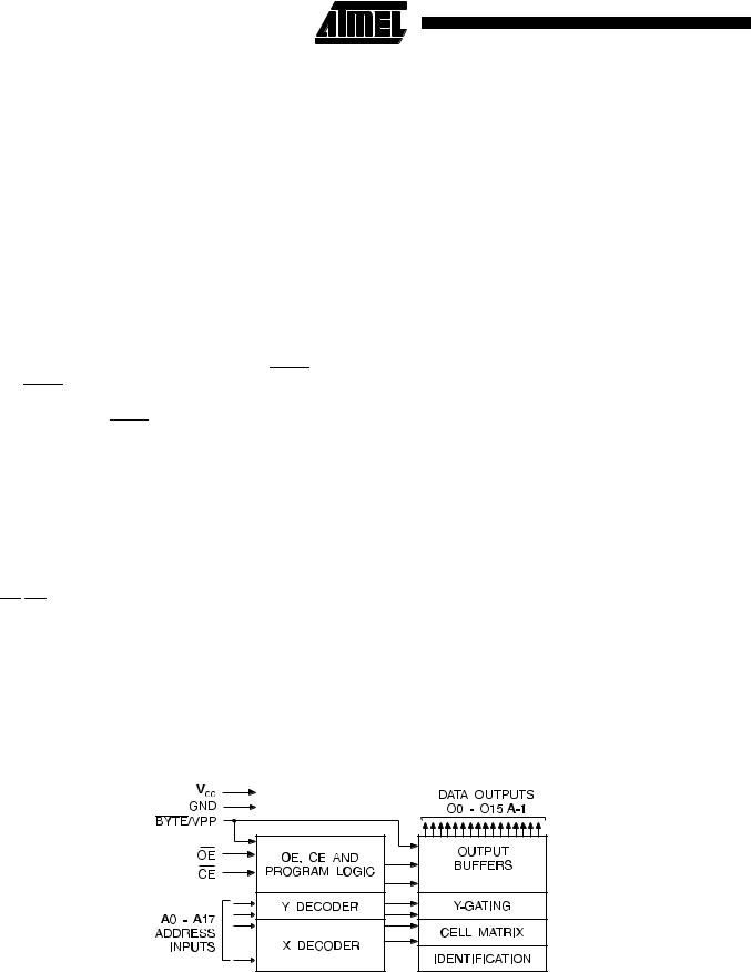
Block Diagram
devices operating at VCC = 5V. At VCC = 2.7V, the part is compatible with JEDEC approved low voltage battery operation (LVBO) interface specifications. The device is also capable of standard 5-volt operation making it ideally suited for dual supply range systems or card products that are pluggable in both 3-volt and 5-volt hosts.
Atmel’s AT27BV400 has additional features that ensure high quality and efficient production use. The RapidTM Programming Algorithm reduces the time required to program the part and guarantees reliable programming. Programming time is typically only 50μs/word. The Integrated Product Identification Code electronically identifies the device and manufacturer. This feature is used by industry standard programming equipment to select the proper programming equipment and voltages. The AT27BV400 programs exactly the same way as a standard 5V AT27C400 and uses the same programming equipment.
System Considerations
Switching between active and standby conditions via the Chip Enable pin may produce transient voltage excursions. Unless accommodated by the system design, these transients may exceed data sheet limits, resulting in device non-conformance. At a minimum, a 0.1 μF high frequency, low inherent inductance, ceramic capacitor should be utilized for each device. This capacitor should be connected between the VCC and Ground terminals of the device, as close to the device as possible. Additionally, to stabilize the supply voltage level on printed circuit boards with large EPROM arrays, a 4.7 μF bulk electrolytic capacitor should be utilized, again connected between the VCC and Ground terminals. This capacitor should be positioned as close as possible to the point where the power supply is connected to the array.
2 |
AT27BV400 |
|
|
||
|

Absolute Maximum Ratings*
Temperature Under Bias |
................................ -55°C to +125°C |
Storage Temperature ..................................... |
-65°C to +150°C |
Voltage on Any Pin with |
-2.0V to +7.0V(1) |
with Respect to Ground .................................. |
|
Voltage on A9 with |
-2.0V to +14.0V(1) |
Respect to Ground ...................................... |
|
VPP Supply Voltage with |
-2.0V to +14.0V(1) |
Respect to Ground ....................................... |
AT27BV400
*NOTICE: Stresses beyond those listed under “Absolute Maximum Ratings” may cause permanent damage to the device. This is a stress rating only and functional operation of the device at these or any other conditions beyond those indicated in the operational sections of this specification is not implied. Exposure to absolute maximum rating conditions for extended periods may affect device reliability.
Note: 1. Minimum voltage is -0.6V DC which undershoot to -2.0V for pulses of less than 20 ns. Maximum output pin voltage is Vcc + 0.75V DC which may overshoot to + 7.0V for pulses of less than 20 ns.
Operating Modes
|
|
|
|
|
|
|
|
|
|
|
|
|
|
|
|
|
|
|
|
Outputs |
|
|
|
|
|
|
|
|
|
|
|
|
|
|
|
|
|
||||||
Mode/Pin |
|
|
|
|
|
|
|
Ai |
|
|
|
|
|
|
|
|
O0-O7 |
O8-O14 |
O15/A-1 |
||
CE |
OE |
|
|
|
BYTE/VPP |
||||||||||||||||
Read Word-wide |
|
V |
|
V |
IL |
X(1) |
|
|
|
V |
IH |
D |
OUT |
D |
D |
||||||
|
|
IL |
|
|
|
|
|
|
|
|
|
|
OUT |
OUT |
|||||||
Read Byte-wide Upper |
|
V |
|
V |
IL |
X(1) |
|
|
|
V |
D |
OUT |
High Z |
V |
|||||||
|
|
IL |
|
|
|
|
|
|
|
|
|
IL |
|
|
IH |
||||||
Read Byte-wide Lower |
|
V |
|
V |
IL |
X(1) |
|
|
|
V |
D |
OUT |
High Z |
V |
|||||||
|
|
IL |
|
|
|
|
|
|
|
|
|
IL |
|
|
IL |
||||||
Output Disable |
X(1) |
|
VIH |
X(1) |
|
|
|
X |
|
|
High Z |
|
|||||||||
Standby |
|
V |
X(1) |
X(1) |
|
|
|
X(6) |
|
|
High Z |
|
|||||||||
|
|
IH |
|
|
|
|
|
|
|
|
|
|
|
|
|
|
|
|
|
|
|
Rapid Program(3) |
|
V |
|
V |
IH |
Ai |
|
|
|
V |
PP |
|
|
D |
|
||||||
|
|
IL |
|
|
|
|
|
|
|
|
|
|
IN |
|
|||||||
PGM Verify |
|
X |
|
VIL |
Ai |
|
|
|
VPP |
|
|
DOUT |
|
||||||||
PGM Inhibit |
|
V |
|
V |
IH |
X(1) |
|
|
|
V |
PP |
|
|
High Z |
|
||||||
|
|
IH |
|
|
|
|
|
|
|
|
|
|
|
|
|||||||
|
|
|
|
|
|
|
|
A9 = V |
(4) |
|
|
|
|
|
|
|
|
|
|
|
|
Product Identification(5) |
|
|
|
|
|
|
|
|
|
H |
|
|
|
|
|
|
|
|
|
|
|
|
V |
|
V |
IL |
A0 = V |
IH |
or V |
IL |
|
V |
IH |
|
Identification Code |
||||||||
|
|
IL |
|
|
|
|
|
|
|
|
|
|
|
||||||||
|
|
|
|
|
|
|
|
A1 - A17 = VIL |
|
|
|
|
|
|
|
|
|
|
|||
Notes: 1. X can be VIL or VIH.
2.Read, output disable, and standby modes require, 2.7V ≤ VCC ≤ 3.6V, or 4.5V ≤ VCC ≤ 5.5V.
3.Refer to the programming characteristics tables in this data sheet.
4.VH = 12.0 ± 0.5V.
5.Two identifier words may be selected. All Ai inputs are held low (VIL) except A9,which is set to VH, and A0, which is toggled low (VIL) to select the Manufacturer’s Identification word and high (VIH) to select the Device Code word.
6.Standby VCC current (ISB) is specified with VPP = VCC. VCC > VPP will cause a slight increase in ISB.
3

DC and AC Operating Conditions for Read Operation
|
|
|
AT27BV400 |
|
|
|
|
|
|
|
|
-12 |
|
-15 |
|
|
|
|
|
Operating Temperature (Case) |
Com. |
0°C - 70°C |
|
0°C - 70°C |
|
|
|
|
|
Ind. |
-40°C - 85°C |
|
-40°C - 85°C |
|
|
|
|||
|
|
|
|
|
VCC Power Supply |
2.7V to 3.6V |
|
2.7V to 3.6V |
|
|
|
|
||
5V ± 10% |
|
5V ± 10% |
||
|
|
|
||
|
|
|
|
|
DC and Operating Characteristics for Read Operation
Symbol |
Parameter |
Condition |
Min |
Max |
Units |
||||||||||||||
|
|
|
|
|
|
|
|
|
|
|
|
|
|
|
|
|
|||
VCC = 2.7V to 3.6V |
|
|
|
|
|
|
|
|
|
|
|
|
|
|
|
||||
ILI |
|
Input Load Current |
VIN = 0V to VCC |
|
±1 |
μA |
|||||||||||||
ILO |
|
Output Leakage Current |
VOUT = 0V to VCC |
|
±5 |
μA |
|||||||||||||
I |
(2) |
V |
(1) |
Read/Standby Current |
V |
PP |
= V |
CC |
|
10 |
μA |
||||||||
PP1 |
|
|
PP |
|
|
|
|
|
|
||||||||||
|
|
|
|
|
ISB1 (CMOS), |
|
|
= VCC ± 0.3V |
|
20 |
μA |
||||||||
I |
|
V |
(1) |
Standby Current |
CE |
|
|||||||||||||
|
|
|
|
|
|
|
|
|
|
|
|
|
|
|
|
||||
|
|
|
|
|
|
|
|
|
|
|
|
|
|
|
|
||||
SB |
|
|
CC |
|
ISB2 (TTL), CE = 2.0 to VCC + 0.5V |
|
100 |
μA |
|||||||||||
|
|
|
|
|
|
||||||||||||||
ICC |
|
VCC Active Current |
f = 5MHz, IOUT = 0 mA, |
|
|
|
= VIL, VCC = 3.6V |
|
10 |
mA |
|||||||||
|
CE |
|
|||||||||||||||||
VIL |
|
Input Low Voltage |
VCC = 3.0 to 3.6V |
-0.6 |
0.8 |
V |
|||||||||||||
|
|
|
|
|
|
|
|
|
|
|
|
|
|
|
|
||||
|
VCC = 2.7 to 3.6V |
-0.6 |
0.2 x VCC |
V |
|||||||||||||||
|
|
|
|
|
|||||||||||||||
|
|
|
|
|
|
|
|
|
|||||||||||
VIH |
|
Input High Voltage |
VCC = 3.0 to 3.6V |
2.0 |
VCC + 0.5 |
V |
|||||||||||||
|
|
|
|
|
|
|
|
|
|
|
|
|
|
|
|
||||
|
VCC = 2.7 to 3.6V |
0.7 x VCC |
VCC + 0.5 |
V |
|||||||||||||||
|
|
|
|
|
|
|
|
|
|||||||||||
|
|
|
|
|
IOL = 2.0 mA |
|
0.4 |
V |
|||||||||||
|
|
|
|
|
|
|
|||||||||||||
VOL |
|
Output Low Voltage |
IOL = 100 μA |
|
0.2 |
V |
|||||||||||||
|
|
|
|
|
IOL = 20 μA |
|
0.1 |
V |
|||||||||||
|
|
|
|
|
|
|
|
|
|||||||||||
|
|
|
|
|
IOH = -2.0 mA |
2.4 |
|
V |
|||||||||||
|
|
|
|
|
|
||||||||||||||
VOH |
Output High Voltage |
IOH = -100 μA |
VCC - 0.2 |
|
V |
||||||||||||||
|
|
|
|
|
IOH = -20 μA |
VCC - 0.1 |
|
V |
|||||||||||
|
|
|
|
|
|
|
|
|
|
|
|
|
|
|
|
|
|||
VCC = 4.5V to 5.5V |
|
|
|
|
|
|
|
|
|
|
|
|
|
|
|
||||
ILI |
|
Input Load Current |
VIN = 0V to VCC |
|
±1 |
μA |
|||||||||||||
ILO |
|
Output Leakage Current |
VOUT = 0V to VCC |
|
±5 |
μA |
|||||||||||||
I |
(2) |
V |
(1) |
Read/Standby Current |
V |
PP |
= V |
CC |
|
10 |
μA |
||||||||
PP1 |
|
|
PP |
|
|
|
|
|
|
||||||||||
|
|
|
|
|
ISB1 (CMOS), |
|
|
= VCC ± 0.3V |
|
100 |
μA |
||||||||
I |
|
V |
(1) |
Standby Current |
CE |
|
|||||||||||||
|
|
|
|
|
|
|
|
|
|
|
|
|
|
|
|
||||
SB |
|
|
CC |
|
ISB2 (TTL), CE = 2.0 to VCC + 0.5V |
|
1 |
mA |
|||||||||||
|
|
|
|
|
|
||||||||||||||
ICC |
|
VCC Active Current |
f = 5 MHz, IOUT = 0 mA, |
|
|
= VIL |
|
40 |
mA |
||||||||||
|
CE |
|
|||||||||||||||||
VIL |
|
Input Low Voltage |
|
|
|
|
|
|
|
|
|
|
|
|
-0.6 |
0.8 |
V |
||
VIH |
|
Input High Voltage |
|
|
|
|
|
|
|
|
|
|
|
|
2.0 |
VCC + 0.5 |
V |
||
VOL |
|
Output Low Voltage |
IOH = 2.1 mA |
|
0.4 |
V |
|||||||||||||
VOH |
Output High Voltage |
IOH = -400 μA |
2.4 |
|
V |
||||||||||||||
Notes: 1. VCC must be applied simultaneously or before VPP, and removed simultaneously or after VPP.
2. VPP may be connected directly to VCC except during programming. The supply current would then be the sum of ICC and IPP.
4 |
AT27BV400 |
|
|
||
|
 Loading...