

Atmel XMEGA B User Manual

8-bit Atmel XMEGA B Microcontroller
XMEGA B MANUAL
This document contains complete and detailed description of all modules included in the
®
AVR®XMEGA® B microcontroller family. The Atmel AVR XMEGA B is a family of low-
Atmel
power, high-performance, and peripheral-rich CMOS 8/16-bit microcontrollers based on the
AVR enhanced RISC architecture with integrated LCD controller. The available Atmel AVR
XMEGA B modules described in this manual are:
Atmel AVR CPU
Memories
DMAC - Direct memory access controller
Event system
System clock and clock options
Power management and sleep modes
System control and reset
WDT - Watchdog timer
Interrupts and programmable multilevel interrupt controller
PORT - I/O ports
TC - 16-bit timer/counters
AWeX - Advanced waveform extension
Hi-Res - High resolution extension
RTC - Real-time counter
USB - Universal serial bus interface
TWI - Two-wire serial interface
SPI - Serial peripheral interface
USART - Universal synchronous and asynchronous serial receiver and transmitter
IRCOM - Infrared communication module
AES and DES cryptographic engine
CRC - Cyclic redundancy check
LCD - Liquid Crystal Display controller
ADC - Analog-to-digital converter
AC - Analog comparator
IEEE 1149.1 JTAG interface
PDI - Program and debug interface
Memory programming
Peripheral address map
Register summary
Interrupt vector summary
Instruction set summary
8291B- AVR-01/2013
8291B–AVR–01/2013

1. About the Manual
This document contains in-depth documentation of all peripherals and modules available for the Atmel AVR XMEGA B
microcontroller family. All features are documented on a functional level and described in a general sense. All peripherals
and modules described in this manual may not be present in all Atmel AVR XMEGA B devices.
For all device-specific information such as characterization data, memory sizes, modules, peripherals available and their
absolute memory addresses, refer to the device datasheets. When several instances of a peripheral exists in one device,
each instance will have a unique name. For example each port module (PORT) have unique name, such as PORTA,
PORTB, etc. Register and bit names are unique within one module instance.
For more details on applied use and code examples for peripherals and modules, refer to the Atmel AVR XMEGA
specific application notes available from http://www.atmel.com/avr.
1.1 Reading the Manual
The main sections describe the various modules and peripherals. Each section contains a short feature list and overview
describing the module. The remaining section describes the features and functions in more detail.
The register description sections list all registers and describe each register, bit and flag with their function. This includes
details on how to set up and enable various features in the module. When multiple bits are needed for a configuration
setting, these are grouped together in a bit group. The possible bit group configurations are listed for all bit groups
together with their associated Group Configuration and a short description. The Group Configuration refers to the defined
configuration name used in the Atmel AVR XMEGA assembler header files and application note source code.
The register summary sections list the internal register map for each module type.
The interrupt vector summary sections list the interrupt vectors and offset address for each module type.
1.2 Resources
A comprehensive set of development tools, application notes, and datasheets are available for download from
http://www.atmel.com/avr.
1.3 Recommended Reading
Atmel AVR XMEGA B device datasheets
AVR XMEGA application notes
This manual contains general modules and peripheral descriptions. The AVR XMEGA B device datasheets contains the device-specific information. The XMEGA application notes and Atmel Software Framework contain example code and show applied use of the modules and peripherals.
For new users, it is recommended to read the AVR1000 - Getting Started Writing C Code for Atmel XMEGA.
XMEGA B [DATASHEET]
8291B–AVR–01/2013
2

2. Overview
The AVR XMEGA B microcontrollers is a family of low-power, high-performance, and peripheral-rich CMOS 8/16-bit
microcontrollers based on the AVR enhanced RISC architecture. By executing powerful instructions in a single clock
cycle, the Atmel AVR XMEGA B devices achieve throughputs approaching one million instructions per second (MIPS)
per megahertz, allowing the system designer to optimize power consumption versus processing speed.
The AVR CPU combines a rich instruction set with 32 general purpose working registers. All 32 registers are directly
connected to the arithmetic logic unit (ALU), allowing two independent registers to be accessed in a single instruction,
executed in one clock cycle. The resulting architecture is more code efficient while achieving throughputs many times
faster than conventional single-accumulator or CISC based microcontrollers.
The Atmel AVR XMEGA B devices provide the following features: in-system programmable flash with read-while-write
capabilities; internal EEPROM and SRAM; two-channel DMA controller; four-channel event system and programmable
multilevel interrupt controller; up to 53 general purpose I/O lines; 16-bit real-time counter (RTC); up to three flexible 16-bit
timer/counters with capture, compare and PWM modes; up to two USARTs; one I
serial interface (TWI); one full-speed USB 2.0 interface; one serial peripheral interface (SPI); one LCD controller
supporting display capacity up to 4 Common and up to 40 Segment terminals; CRC module; AES and DES cryptographic
engine; up to two 8-channel, 12-bit ADCs with programmable gain; up to four analog comparators with window mode;
programmable watchdog timer with separate internal oscillator; accurate internal oscillators with PLL and prescaler; and
programmable brown-out detection.
The program and debug interface (PDI), a fast, two-pin interface for programming and debugging, is available. Selected
devices also have an IEEE std. 1149.1 compliant JTAG interface, and this can also be used for on-chip debug and
programming.
The Atmel AVR XMEGA devices have five software selectable power saving modes. The idle mode stops the CPU while
allowing the SRAM, DMA controller, event system, interrupt controller, and all peripherals to continue functioning. The
power-down mode saves the SRAM and register contents, but stops the oscillators, disabling all other functions until the
next TWI, USB resume, or pin-change interrupt, or reset. In power-save mode, the asynchronous real-time counter
continues to run, allowing the application to maintain a timer base while the rest of the device is sleeping. In this mode,
the LCD controller is allowed to refresh data to the panel. In standby mode, the external crystal oscillator keeps running
while the rest of the device is sleeping. This allows very fast startup from the external crystal, combined with low power
consumption. In extended standby mode, both the main oscillator and the asynchronous timer continue to run. In this
mode, the LCD controller is allowed to refresh data to the panel. To further reduce power consumption, the peripheral
clock to each individual peripheral can optionally be stopped in active mode and idle sleep mode.
The devices are manufactured using Atmel high-density, nonvolatile memory technology. The program flash memory can
be reprogrammed in-system through the PDI or JTAG interfaces. A boot loader running in the device can use any
interface to download the application program to the flash memory. The boot loader software in the boot flash section will
continue to run while the application flash section is updated, providing true read-while-write operation. By combining an
8/16-bit RISC CPU with In-system, self-programmable flash, the Atmel AVR XMEGA is a powerful microcontroller family
that provides a highly flexible and cost effective solution for many embedded applications.
The Atmel AVR XMEGA B devices are supported with a full suite of program and system development tools, including C
compilers, macro assemblers, program debugger/simulators, programmers, and evaluation kits.
2
C and SMBUS compatible two-wire
XMEGA B [DATASHEET]
8291B–AVR–01/2013
3
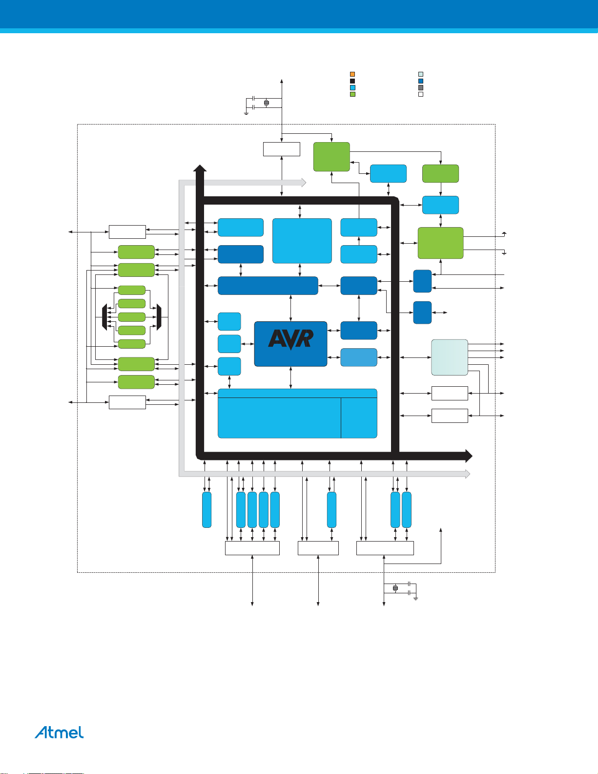
Figure 2-1. Atmel AVR XMEGA B block diagram.
XTAL1 /
TOSC1
XTAL2 /
TOSC2
PR[0..1]
Ground
Digital function
Analog function / Oscillators
LCDPower
Programming, debug, test
External clock / Crystal pins
General Purpose I/O
PA[0..7]
PB[0..7]/
JTAG
PORT A (8)
ACA
ADCA
AREFA
VCC/10
Int. Refs.
Tempref
AREFB
ADCB
ACB
PORT B (8)
PORT R (2)
EVENT ROUTING NETWORK
Event System
Controller
DMA
Controller
BUS Matrix
AES
DES
CRC
Oscillator
Circuits/
Clock
Generation
DATA BUS
Oscillator
Control
SRAM
Sleep
Controller
Prog/Debug
Controller
OCD
CPU
NVM Controller
Flash EEPROM
Interrupt
Controller
Real Time
Counter
Watchdog
Oscillator
Watchdog
Supervision
POR/BOD &
PDI
JTAG
Timer
Power
RESET
PORT B
LCD
PORT M (8)
PORT G (8)
VCC
GND
RESET /
PDI_CLK
PDI_DATA
LCD POWER[0..4]
COM[0..3]
SEG[0..23]
SEG[31..24] /
PM[0..7]
SEG[39..32] /
PG[0..7]
DATA BUS
EVENT ROUTING NETWORK
IRCOM
TCC0:1
USARTC0
PORT C (8)
PC[0..7]
SPIC
TWIC
PORT D (3)
USB
PORT E (8)
PD[0..2] PE[0..7]
TCE0
TOSC1
TOSC2
USARTE0
(Alternate)
To Clock
Generator
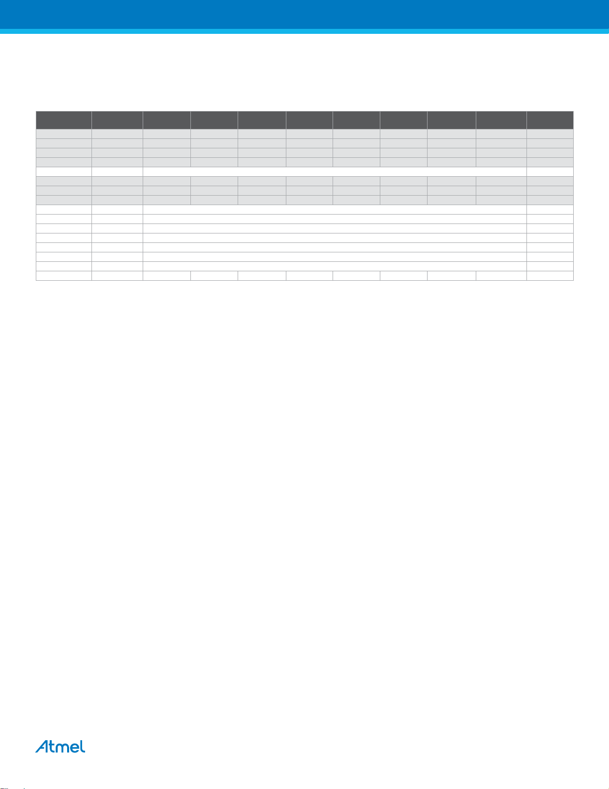
In Table 2-1 on page 5 a feature summary for the XMEGA B family is shown, split into one feature summary column for
each sub-family. Each sub-family has identical feature set, but different memory options, refer to their device datasheet
for ordering codes and memory options.
XMEGA B [DATASHEET]
8291B–AVR–01/2013
4

Table 2-1. XMEGA B feature summary overview.
Feature Details / sub-family B1 B3
Pins, I/O
Total 100 64
Programmable I/O pins 53 36
Program memory (KB) 64 - 128 64 - 128
Boot memory (KB) 4 - 8 4 - 8
Memory
SRAM (KB) 4 - 8 4 - 8
EEPROM 2 2 - 4
General purpose registers 16 16
TQFP 100A 64A
Package
QFN /VQFN – 64M2
BGA 100C1/100C2 –
QTouch Sense channels 56 56
DMA Controller Channels 2 2
Channels 4 4
Event System
QDEC 1 1
0.4 - 16MHz XOSC Yes Ye s
Crystal Oscillator
32.768 kHz TOSC Yes Yes
Internal Oscillator
Timer / Counter
Serial Communication
2MHz calibrated Yes Yes
32MHz calibrated Yes Yes
128MHz PLL Yes Yes
32.768kHz calibrated Yes Ye s
32kHz ULP Yes Yes
TC0 - 16-bit, 4 CC 2 1
TC1 - 16-bit, 2 CC 1 1
TC2 - 2x 8-bit 2 1
Hi-Res 1 1
AWeX 1 1
RTC 1 1
RTC32
USB full-speed device 1 1
USART 2 1
SPI 1 1
TWI 1 1
XMEGA B [DATASHEET]
8291B–AVR–01/2013
5

Feature Details / sub-family B1 B3
AES-128 Yes Yes
Crypto /CRC
DES Yes Yes
CRC-16 Ye s Yes
CRC-32 Ye s Yes
Liquid Crystal Display
Controller (LCD)
Segments 40 25
Common terminals 4 4
2 1
Resolution (bits) 12 12
Analog to Digital Converter
(ADC)
Sampling speed (kbps) 300 300
Input channels per ADC 16 8
Conversion channels 1 1
Analog Comparator (AC) 4 2
PDI Yes Yes
Program and Debug Interface
JTAG Ye s Ye s
Boundary scan Yes Yes
XMEGA B [DATASHEET]
8291B–AVR–01/2013
6
3. Atmel AVR CPU
3.1 Features
8/16-bit, high-performance Atmel AVR RISC CPU
142 instructions
Hardware multiplier
32x8-bit registers directly connected to the ALU
Stack in RAM
Stack pointer accessible in I/O memory space
Direct addressing of up to 16MB of program memory and 16MB of data memory
True 16/24-bit access to 16/24-bit I/O registers
Efficient support for 8-, 16-, and 32-bit arithmetic
Configuration change protection of system-critical features
3.2 Overview
All Atmel AVR XMEGA devices use the 8/16-bit AVR CPU. The main function of the CPU is to execute the code and
perform all calculations. The CPU is able to access memories, perform calculations, control peripherals, and execute the
program in the flash memory. Interrupt handling is described in a separate section, “Interrupts and Programmable
Multilevel Interrupt Controller” on page 118.
3.3 Architectural Overview
In order to maximize performance and parallelism, the AVR CPU uses a Harvard architecture with separate memories
and buses for program and data. Instructions in the program memory are executed with single-level pipelining. While one
instruction is being executed, the next instruction is pre-fetched from the program memory. This enables instructions to
be executed on every clock cycle. For a summary of all AVR instructions, refer to “Instruction Set Summary” on page
397. For details of all AVR instructions, refer to http://www.atmel.com/avr.
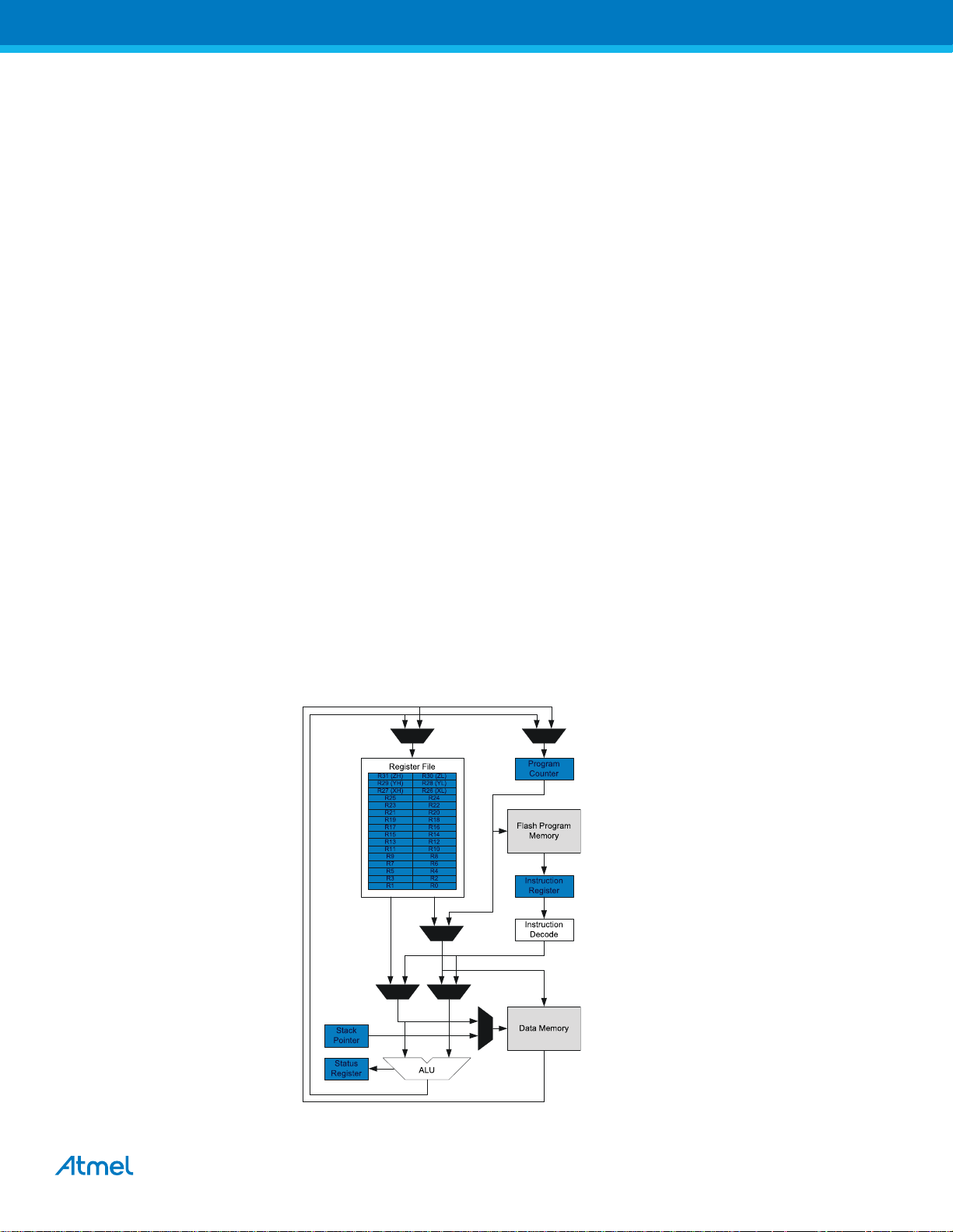
Figure 3-1. Block diagram of the AVR CPU architecture.
XMEGA B [DATASHEET]
8291B–AVR–01/2013
7

The arithmetic logic unit (ALU) supports arithmetic and logic operations between registers or between a constant and a
register. Single-register operations can also be executed in the ALU. After an arithmetic operation, the status register is
updated to reflect information about the result of the operation.
The ALU is directly connected to the fast-access register file. The 32 x 8-bit general purpose working registers all have
single clock cycle access time allowing single-cycle arithmetic logic unit operation between registers or between a
register and an immediate. Six of the 32 registers can be used as three 16-bit address pointers for program and data
space addressing, enabling efficient address calculations.
The memory spaces are linear. The data memory space and the program memory space are two different memory
spaces.
The data memory space is divided into I/O registers, SRAM, and external RAM. In addition, the EEPROM can be
memory mapped in the data memory.
All I/O status and control registers reside in the lowest 4KB addresses of the data memory. This is referred to as the I/O
memory space. The lowest 64 addresses can be accessed directly, or as the data space locations from 0x00 to 0x3F.
The rest is the extended I/O memory space, ranging from 0x0040 to 0x0FFF. I/O registers here must be accessed as
data space locations using load (LD/LDS/LDD) and store (ST/STS/STD) instructions.
The SRAM holds data. Code execution from SRAM is not supported. It can easily be accessed through the five different
addressing modes supported in the AVR architecture. The first SRAM address is 0x2000.
Data addresses 0x1000 to 0x1FFF are reserved for memory mapping of EEPROM.
The program memory is divided in two sections, the application program section and the boot program section. Both
sections have dedicated lock bits for write and read/write protection. The SPM instruction that is used for selfprogramming of the application flash memory must reside in the boot program section. The application section contains
an application table section with separate lock bits for write and read/write protection. The application table section can
be used for save storing of nonvolatile data in the program memory.
3.4 ALU - Arithmetic Logic Unit
The arithmetic logic unit supports arithmetic and logic operations between registers or between a constant and a register.
Single-register operations can also be executed. The ALU operates in direct connection with all 32 general purpose
registers. In a single clock cycle, arithmetic operations between general purpose registers or between a register and an
immediate are executed and the result is stored in the register file. After an arithmetic or logic operation, the status
register is updated to reflect information about the result of the operation.
ALU operations are divided into three main categories – arithmetic, logical, and bit functions. Both 8- and 16-bit
arithmetic is supported, and the instruction set allows for efficient implementation of 32-bit arithmetic. The hardware
multiplier supports signed and unsigned multiplication and fractional format.
3.4.1 Hardware Multiplier
The multiplier is capable of multiplying two 8-bit numbers into a 16-bit result. The hardware multiplier supports different
variations of signed and unsigned integer and fractional numbers:
Multiplication of unsigned integers
Multiplication of signed integers
Multiplication of a signed integer with an unsigned integer
Multiplication of unsigned fractional numbers
Multiplication of signed fractional numbers
Multiplication of a signed fractional number with an unsigned one
A multiplication takes two CPU clock cycles.
XMEGA B [DATASHEET]
8291B–AVR–01/2013
8
3.5 Program Flow
2
4th Instruction Fetch
T1 T2 T3 T4
After reset, the CPU starts to execute instructions from the lowest address in the flash program memory ‘0.’ The program
counter (PC) addresses the next instruction to be fetched.
Program flow is provided by conditional and unconditional jump and call instructions capable of addressing the whole
address space directly. Most AVR instructions use a 16-bit word format, while a limited number use a 32-bit format.
During interrupts and subroutine calls, the return address PC is stored on the stack. The stack is allocated in the general
data SRAM, and consequently the stack size is only limited by the total SRAM size and the usage of the SRAM. After
reset, the stack pointer (SP) points to the highest address in the internal SRAM. The SP is read/write accessible in the
I/O memory space, enabling easy implementation of multiple stacks or stack areas. The data SRAM can easily be
accessed through the five different addressing modes supported in the AVR CPU.
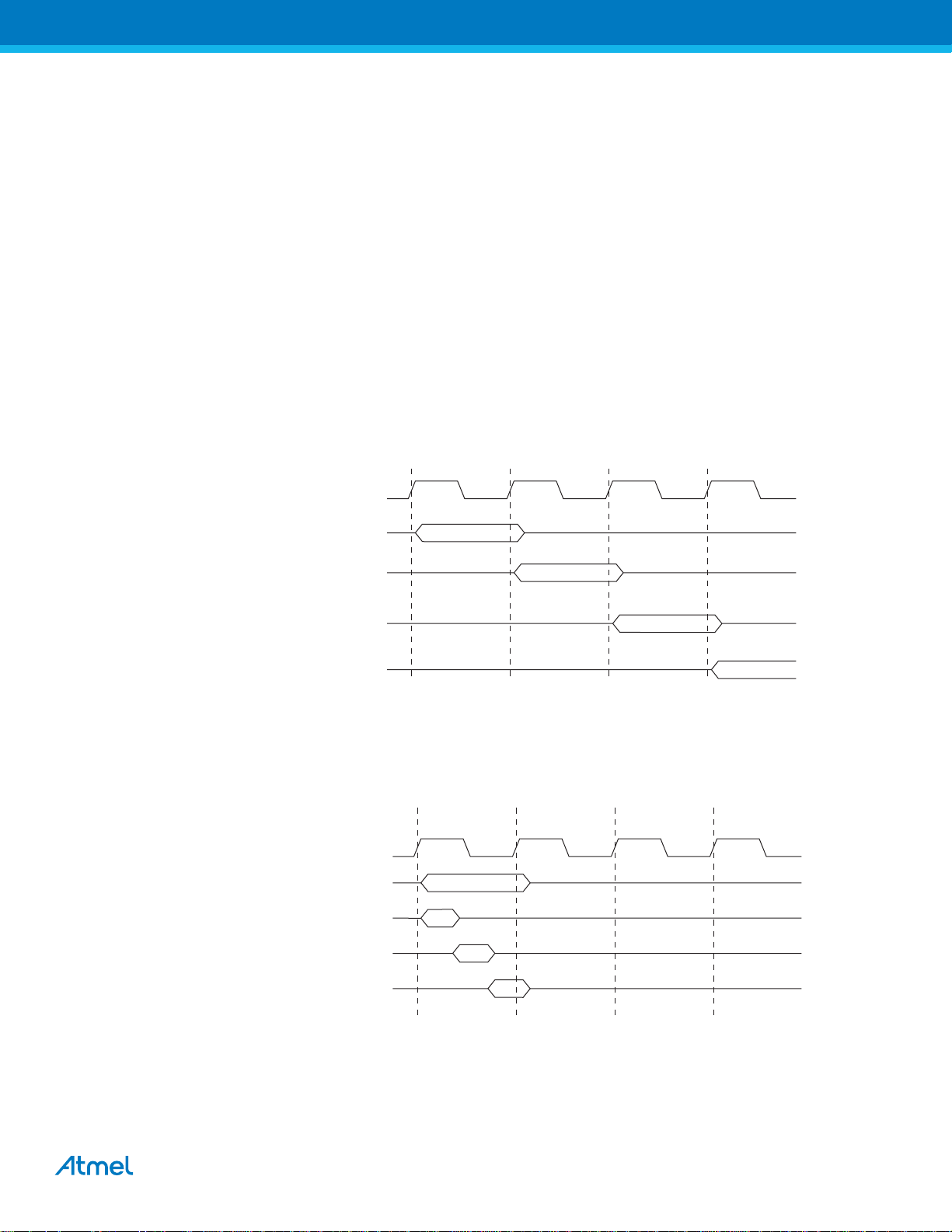
3.6 Instruction Execution Timing
The AVR CPU is clocked by the CPU clock, clk
. No internal clock division is used. Figure 3-2 on page 9 shows the
CPU
parallel instruction fetches and instruction executions enabled by the Harvard architecture and the fast-access register
file concept. This is the basic pipelining concept used to obtain up to 1MIPS/MHz performance with high power efficiency.
Figure 3-2. The parallel instruction fetches and instruction executions.
clk
CPU
1st Instruction Fetch
1st Instruction Execute
2nd Instruction Fetch
nd Instruction Execute
3rd Instruction Fetch
3rd Instruction Execute
Figure 3-3 on page 9 shows the internal timing concept for the register file. In a single clock cycle, an ALU operation
using two register operands is executed and the result is stored back to the destination register.
Figure 3-3. Single Cycle ALU Operation
T1 T2 T3 T4
clk
CPU
Total Execution Time
Register Operands Fetch
ALU Operation Execute
Result Write Back
XMEGA B [DATASHEET]
8291B–AVR–01/2013
9

3.7 Status Register
The status register (SREG) contains information about the result of the most recently executed arithmetic or logic
instruction. This information can be used for altering program flow in order to perform conditional operations. Note that
the status register is updated after all ALU operations, as specified in the instruction set reference. This will in many
cases remove the need for using the dedicated compare instructions, resulting in faster and more compact code.
The status register is not automatically stored when entering an interrupt routine nor restored when returning from an
interrupt. This must be handled by software.
The status register is accessible in the I/O memory space.
3.8 Stack and Stack Pointer
The stack is used for storing return addresses after interrupts and subroutine calls. It can also be used for storing
temporary data. The stack pointer (SP) register always points to the top of the stack. It is implemented as two 8-bit
registers that are accessible in the I/O memory space. Data are pushed and popped from the stack using the PUSH and
POP instructions. The stack grows from a higher memory location to a lower memory location. This implies that pushing
data onto the stack decreases the SP, and popping data off the stack increases the SP. The SP is automatically loaded
after reset, and the initial value is the highest address of the internal SRAM. If the SP is changed, it must be set to point
above address 0x2000, and it must be defined before any subroutine calls are executed or before interrupts are enabled.
During interrupts or subroutine calls, the return address is automatically pushed on the stack. The return address can be
two or three bytes, depending on program memory size of the device. For devices with 128KB or less of program
memory, the return address is two bytes, and hence the stack pointer is decremented/incremented by two. For devices
with more than 128KB of program memory, the return address is three bytes, and hence the SP is
decremented/incremented by three. The return address is popped off the stack when returning from interrupts using the
RETI instruction, and from subroutine calls using the RET instruction.
The SP is decremented by one when data are pushed on the stack with the PUSH instruction, and incremented by one
when data is popped off the stack using the POP instruction.
To prevent corruption when updating the stack pointer from software, a write to SPL will automatically disable interrupts
for up to four instructions or until the next I/O memory write.
3.9 Register File
The register file consists of 32 x 8-bit general purpose working registers with single clock cycle access time. The register
file supports the following input/output schemes:
One 8-bit output operand and one 8-bit result input
Two 8-bit output operands and one 8-bit result input
Two 8-bit output operands and one 16-bit result input
One 16-bit output operand and one 16-bit result input
Six of the 32 registers can be used as three 16-bit address register pointers for data space addressing, enabling efficient
address calculations. One of these address pointers can also be used as an address pointer for lookup tables in flash
program memory.
XMEGA B [DATASHEET]
8291B–AVR–01/2013
10
Figure 3-4. AVR CPU general purpose working registers.
7 0 Addr.
R0 0x00
R1 0x01
R2 0x02
…
R13 0x0D
General R14 0x0E
Purpose R15 0x0F
Working R16 0x10
Registers R17 0x11
…
R26 0x1A X-register Low Byte
R27 0x1B X-register High Byte
R28 0x1C Y-register Low Byte
R29 0x1D Y-register High Byte
R30 0x1E Z-register Low Byte
R31 0x1F Z-register High Byte
The register file is located in a separate address space, and so the registers are not accessible as data memory.
3.9.1 The X-, Y-, and Z- Registers
Registers R26..R31 have added functions besides their general-purpose usage.
These registers can form 16-bit address pointers for addressing data memory. These three address registers are called
the X-register, Y-register, and Z-register. The Z-register can also be used as an address pointer to read from and/or write
to the flash program memory, signature rows, fuses, and lock bits.
Figure 3-5. The X-, Y- and Z-registers.
Bit (individually) 7 R27 0 7 R26 0
X-register XH XL
Bit (X-register) 15 8 7 0
Bit (individually) 7 R29 0 7 R28 0
Y-register YH YL
Bit (Y-register) 15 8 7 0
Bit (individually) 7 R31 0 7 R30 0
Z-register ZH ZL
Bit (Z-register) 15 8 7 0
XMEGA B [DATASHEET]
8291B–AVR–01/2013
11

The lowest register address holds the least-significant byte (LSB), and the highest register address holds the mostsignificant byte (MSB). In the different addressing modes, these address registers function as fixed displacement,
automatic increment, and automatic decrement (see the instruction set reference for details).
3.10 RAMP and Extended Indirect Registers
In order to access program memory or data memory above 64KB, the address pointer must be larger than 16 bits. This is
done by concatenating one register to one of the X-, Y-, or Z-registers. This register then holds the most-significant byte
(MSB) in a 24-bit address or address pointer.
These registers are available only on devices with external bus interface and/or more than 64KB of program or data
memory space. For these devices, only the number of bits required to address the whole program and data memory
space in the device is implemented in the registers.
3.10.1 RAMPX, RAMPY and RAMPZ Registers
The RAMPX, RAMPY and RAMPZ registers are concatenated with the X-, Y-, and Z-registers, respectively, to enable
indirect addressing of the whole data memory space above 64KB and up to 16MB.
Figure 3-6. The combined RAMPX + X, RAMPY + Y and RAMPZ + Z registers.
Bit (Individually) 7 0 7 0 7 0
RAMPX XH XL
Bit (X-pointer) 23 16 15 8 7 0
Bit (Individually) 7 0 7 0 7 0
Bit (Y-pointer) 23 16 15 8 7 0
Bit (Individually) 7 0 7
Bit (Z-pointer) 23 16 15 8 7 0
When reading (ELPM) and writing (SPM) program memory locations above the first 128KB of the program memory,
RAMPZ is concatenated with the Z-register to form the 24-bit address. LPM is not affected by the RAMPZ setting.
3.10.2 RAMPD Register
This register is concatenated with the operand to enable direct addressing of the whole data memory space above 64KB.
Together, RAMPD and the operand will form a 24-bit address.
Figure 3-7. The combined RAMPD + K register.
Bit (Individually) 7 0 15 0
Bit (D-pointer) 23 16 15 0
RAMPY YH YL
70
0
RAMPZ ZH ZL
RAMPD K
XMEGA B [DATASHEET]
8291B–AVR–01/2013
12

3.10.3 EIND - Extended Indirect Register
EIND is concatenated with the Z-register to enable indirect jump and call to locations above the first 128KB (64K words)
of the program memory.
Figure 3-8. The combined EIND + Z register.
Bit (Individually) 7 0 7
EIND ZH ZL
Bit (D-pointer) 23 16 15 8 7 0
3.11 Accessing 16-bit Registers
The AVR data bus is 8 bits wide, and so accessing 16-bit registers requires atomic operations. These registers must be
byte-accessed using two read or write operations. 16-bit registers are connected to the 8-bit bus and a temporary register
using a 16-bit bus.
For a write operation, the low byte of the 16-bit register must be written before the high byte. The low byte is then written
into the temporary register. When the high byte of the 16-bit register is written, the temporary register is copied into the
low byte of the 16-bit register in the same clock cycle.
For a read operation, the low byte of the 16-bit register must be read before the high byte. When the low byte register is
read by the CPU, the high byte of the 16-bit register is copied into the temporary register in the same clock cycle as the
low byte is read. When the high byte is read, it is then read from the temporary register.
This ensures that the low and high bytes of 16-bit registers are always accessed simultaneously when reading or writing
the register.
Interrupts can corrupt the timed sequence if an interrupt is triggered and accesses the same 16-bit register during an
atomic 16-bit read/write operation. To prevent this, interrupts can be disabled when writing or reading 16-bit registers.
The temporary registers can also be read and written directly from user software.
3.11.1 Accessing 24- and 32-bit Registers
70
0
For 24- and 32-bit registers, the read and write access is done in the same way as described for 16-bit registers, except
there are two temporary registers for 24-bit registers and three for 32-bit registers. The least-significant byte must be
written first when doing a write, and read first when doing a read.
3.12 Configuration Change Protection
System critical I/O register settings are protected from accidental modification. The SPM instruction is protected from
accidental execution, and the LPM instruction is protected when reading the fuses and signature row. This is handled
globally by the configuration change protection (CCP) register. Changes to the protected I/O registers or bits, or
execution of protected instructions, are only possible after the CPU writes a signature to the CCP register. The different
signatures are described in the register description.
There are two modes of operation: one for protected I/O registers, and one for the protected instructions, SPM/LPM.
3.12.1 Sequence for write operation to protected I/O registers
1. The application code writes the signature that enable change of protected I/O registers to the CCP register.
2. Within four instruction cycles, the application code must write the appropriate data to the protected register. Most
protected registers also contain a write enable/change enable bit. This bit must be written to one in the same operation as the data are written. The protected change is immediately disabled if the CPU performs write operations to
the I/O register or data memory or if the SPM, LPM, or SLEEP instruction is executed.
XMEGA B [DATASHEET]
8291B–AVR–01/2013
13

3.12.2 Sequence for execution of protected SPM/LPM
1. The application code writes the signature for the execution of protected SPM/LPM to the CCP register.
2. Within four instruction cycles, the application code must execute the appropriate instruction. The protected change
is immediately disabled if the CPU performs write operations to the data memory or if the SLEEP instruction is
executed.
Once the correct signature is written by the CPU, interrupts will be ignored for the duration of the configuration change
enable period. Any interrupt request (including non-maskable interrupts) during the CCP period will set the
corresponding interrupt flag as normal, and the request is kept pending. After the CCP period is completed, any pending
interrupts are executed according to their level and priority. DMA requests are still handled, but do not influence the
protected configuration change enable period. A signature written by DMA is ignored.
3.13 Fuse Lock
For some system-critical features, it is possible to program a fuse to disable all changes to the associated I/O control
registers. If this is done, it will not be possible to change the registers from the user software, and the fuse can only be
reprogrammed using an external programmer. Details on this are described in the datasheet module where this feature is
available.
XMEGA B [DATASHEET]
8291B–AVR–01/2013
14
3.14 Register Descriptions
3.14.1 CCP – Configuration Change Protection register
Bit 76543210
+0x04 CCP[7:0]
Read/Write W W W W W W R/W R/W
Initial Value 0 0 0 0 0 0 0 0
Bit 7:0 – CCP[7:0]: Configuration Change Protection
The CCP register must be written with the correct signature to enable change of the protected I/O register or execution of
the protected instruction for a maximum period of four CPU instruction cycles. All interrupts are ignored during these
cycles. After these cycles, interrupts will automatically be handled again by the CPU, and any pending interrupts will be
executed according to their level and priority. When the protected I/O register signature is written, CCP[0] will read as
one as long as the protected feature is enabled. Similarly when the protected SPM/LPM signature is written, CCP[1] will
read as one as long as the protected feature is enabled. CCP[7:2] will always read as zero. Table 3-1 shows the
signature for the various modes.
Table 3-1. Modes of CPU change protection.
Signature Group Configuration Description
0x9D SPM Protected SPM/LPM
0xD8 IOREG Protected IO register
3.14.2 RAMPD – Extended Direct Addressing register
This register is concatenated with the operand for direct addressing (LDS/STS) of the whole data memory space on
devices with more than 64KB of data memory. This register is not available if the data memory, including external
memory, is less than 64KB.
Bit 76543210
+0x08 RAMPD[7:0]
Read/Write R/W R/W R/W R/W R/W R/W R/W R/W
Initial Value 0 0 0 0 0 0 0 0
Bit 7:0 – RAMPD[7:0]: Extended Direct Addressing bits
These bits hold the MSB of the 24-bit address created by RAMPD and the 16-bit operand. Only the number of bits
required to address the available data memory is implemented for each device. Unused bits will always read as zero.
XMEGA B [DATASHEET]
8291B–AVR–01/2013
15
3.14.3 RAMPX – Extended X-Pointer register
This register is concatenated with the X-register for indirect addressing (LD/LDD/ST/STD) of the whole data memory
space on devices with more than 64KB of data memory. This register is not available if the data memory, including
external memory, is less than 64KB.
Bit 76543210
+0x09 RAMPX[7:0]
Read/Write R/W R/W R/W R/W R/W R/W R/W R/W
Initial Value 0 0 0 0 0 0 0 0
Bit 7:0 – RAMPX[7:0]: Extended X-pointer Address bits
These bits hold the MSB of the 24-bit address created by RAMPX and the 16-bit X-register. Only the number of bits
required to address the available data memory is implemented for each device. Unused bits will always read as zero.
3.14.4 RAMPY – Extended Y-Pointer register
This register is concatenated with the Y-register for indirect addressing (LD/LDD/ST/STD) of the whole data memory
space on devices with more than 64KB of data memory. This register is not available if the data memory, including
external memory, is less than 64KB.
Bit 76543210
+0x0A RAMPY[7:0]
Read/Write R/W R/W R/W R/W R/W R/W R/W R/W
Initial Value 0 0 000000
Bit 7:0 – RAMPY[7:0]: Extended Y-pointer Address bits
These bits hold the MSB of the 24-bit address created by RAMPY and the 16-bit Y-register. Only the number of bits
required to address the available data memory is implemented for each device. Unused bits will always read as zero.
3.14.5 RAMPZ – Extended Z-Pointer register
This register is concatenated with the Z-register for indirect addressing (LD/LDD/ST/STD) of the whole data memory
space on devices with more than 64KB of data memory. RAMPZ is concatenated with the Z-register when reading
(ELPM) program memory locations above the first 64KB and writing (SPM) program memory locations above the first
128KB of the program memory.
This register is not available if the data memory, including external memory and program memory in the device, is less
than 64KB.
Bit 76543210
+0x0B RAMPZ[7:0]
Read/Write R/W R/W R/W R/W R/W R/W R/W R/W
Initial Value 00000000
Bit 7:0 – RAMPZ[7:0]: Extended Z-pointer Address bits
These bits hold the MSB of the 24-bit address created by RAMPZ and the 16-bit Z-register. Only the number of bits
required to address the available data and program memory is implemented for each device. Unused bits will always
read as zero.
XMEGA B [DATASHEET]
8291B–AVR–01/2013
16
3.14.6 EIND – Extended Indirect register
This register is concatenated with the Z-register for enabling extended indirect jump (EIJMP) and call (EICALL) to the
whole program memory space on devices with more than 128KB of program memory. The register should be used for
jumps to addresses below 128KB if ECALL/EIJMP are used, and it will not be used if CALL and IJMP commands are
used. For jump or call to addresses below 128KB, this register is not used. This register is not available if the program
memory in the device is less than 128KB.
Bit 76543210
+0x0C EIND[7:0]
Read/Write R/W R/W R/W R/W R/W R/W R/W R/W
Initial Value 0 0 0 0 0 0 0 0
Bit 7:0 – EIND[7:0]: Extended Indirect Address bits
These bits hold the MSB of the 24-bit address created by EIND and the 16-bit Z-register. Only the number of bits
required to access the available program memory is implemented for each device. Unused bits will always read as zero.
3.14.7 SPL – Stack Pointer Register Low
The SPH and SPL register pair represent the 16-bit SP value. The SP holds the stack pointer that points to the top of the
stack. After reset, the stack pointer points to the highest internal SRAM address. To prevent corruption when updating
the stack pointer from software, a write to SPL will automatically disable interrupts for the next four instructions or until
the next I/O memory write.
Only the number of bits required to address the available data memory, including external memory, up to 64KB is
implemented for each device. Unused bits will always read as zero.
Bit 76543210
+0x0D SP[7:0]
Read/Write R/W R/W R/W R/W R/W R/W R/W R/W
Initial Value
Note: 1. Refer to specific device datasheets for exact initial values.
Bit 7:0 – SP[7:0]: Stack Pointer Register Low
(1)
0/1 0/1 0/1 0/1 0/1 0/1 0/1 0/1
These bits hold the LSB of the 16-bit stack pointer (SP).
3.14.8 SPH – Stack Pointer Register High
Bit 76543210
+0x0E SP[15:8]
Read/Write R/W R/W R/W R/W R/W R/W R/W R/W
Initial Value
Note: 1. Refer to specific device datasheets for exact initial values.
Bit 7:0 – SP[15:8]: Stack Pointer Register High
(1)
0/1 0/1 0/1 0/1 0/1 0/1 0/1 0/1
These bits hold the MSB of the 16-bit stack pointer (SP).
XMEGA B [DATASHEET]
8291B–AVR–01/2013
17

3.14.9 SREG – Status Register
The status register (SREG) contains information about the result of the most recently executed arithmetic or logic
instruction.
Bit 76543210
+0x0F ITHSVNZC
Read/Write R/W R/W R/W R/W R/W R/W R/W R/W
Initial Value 0 0 0 0 0 0 0 0
Bit 7 – I: Global Interrupt Enable
The global interrupt enable bit must be set for interrupts to be enabled. If the global interrupt enable register is cleared,
none of the interrupts are enabled independent of the individual interrupt enable settings. This bit is not cleared by
hardware after an interrupt has occurred. This bit can be set and cleared by the application with the SEI and CLI
instructions, as described in “Instruction Set Description.” Changing the I flag through the I/O-register result in a onecycle wait state on the access.
Bit 6 – T: Bit Copy Storage
The bit copy instructions bit load (BLD) and bit store (BST) use the T bit as source or destination for the operated bit. A bit
from a register in the register file can be copied into this bit by the BST instruction, and this bit can be copied into a bit in
a register in the register file by the BLD instruction.
Bit 5 – H: Half Carry Flag
The half carry flag (H) indicates a half carry in some arithmetic operations. Half carry Is useful in BCD arithmetic. See
“Instruction Set Description” for detailed information.
Bit 4 – S: Sign Bit, S = N V
The sign bit is always an exclusive or between the negative flag, N, and the two’s complement overflow flag, V. See
“Instruction Set Description” for detailed information.
Bit 3 – V: Two’s Complement Overflow Flag
The two’s complement overflow flag (V) supports two’s complement arithmetic. See “Instruction Set Description” for
detailed information.
Bit 2 – N: Negative Flag
The negative flag (N) indicates a negative result in an arithmetic or logic operation. See “Instruction Set Description” for
detailed information.
Bit 1 – Z: Zero Flag
The zero flag (Z) indicates a zero result in an arithmetic or logic operation. See “Instruction Set Description” for detailed
information.
Bit 0 – C: Carry Flag
The carry flag (C) indicates a carry in an arithmetic or logic operation. See “Instruction Set Description” for detailed
information.
XMEGA B [DATASHEET]
8291B–AVR–01/2013
18
3.15 Register Summary
Address Name Bit 7 Bit 6 Bit 5 Bit 4 Bit 3 Bit 2 Bit 1 Bit 0 Page
+0x00 Reserved – – – – – – – –
+0x01 Reserved – – – – – – – –
+0x02 Reserved – – – – – – – –
+0x03 Reserved – – – – – – – –
+0x04 CCP CCP[7:0] 15
+0x05 Reserved – – – – – – – –
+0x06 Reserved – – – – – – – –
+0x07 Reserved – – – – – – – –
+0x08 RAMPD RAMPD[7:0] 15
+0x09 RAMPX RAMPX[7:0] 16
+0x0A RAMPY RAMPY[7:0] 16
+0x0B RAMPZ RAMPZ[7:0] 16
+0x0C EIND EIND[7:0] 17
+0x0D SPL SPL[7:0] 17
+0x0E SPH SPH[7:0] 17
+0x0F SREG I T H S V N Z C 18
XMEGA B [DATASHEET]
8291B–AVR–01/2013
19

4. Memories
4.1 Features
Flash program memory
One linear address space
In-system programmable
Self-programming and boot loader support
Application section for application code
Application table section for application code or data storage
Boot section for application code or bootloader code
Separate read/write protection lock bits for all sections
Built in fast CRC check of a selectable flash program memory section
Data memory
One linear address space
Single-cycle access from CPU
SRAM
EEPROM
Byte and page accessible
Optional memory mapping for direct load and store
I/O memory
Configuration and status registers for all peripherals and modules
16 bit-accessible general purpose registers for global variables or flags
Bus arbitration
Safe and deterministic handling of priority between CPU, DMA controller, and other bus masters
Separate buses for SRAM, EEPROM and I/O memory access
Simultaneous bus access for CPU and DMA controller
Production signature row memory for factory programmed data
ID for each microcontroller device type
Serial number for each device
Calibration bytes for factory calibrated peripherals
User signature row
One flash page in size
Can be read and written from software
Content is kept after chip erase
4.2 Overview
This section describes the different memory sections. The AVR architecture has two main memory spaces, the program
memory and the data memory. Executable code can reside only in the program memory, while data can be stored in the
program memory and the data memory. The data memory includes the internal SRAM, and as well as EEPROM for
nonvolatile data storage. All memory spaces are linear and require no memory bank switching. Nonvolatile memory
(NVM) spaces can be locked for further write and read/write operations. This prevents unrestricted access to the
application software.
A separate memory section contains the fuse bytes. These are used for configuring important system functions, and can
only be written by an external programmer.
4.3 Flash Program Memory
All XMEGA devices contain on-chip, in-system reprogrammable flash memory for program storage. The flash memory
can be accessed for read and write from an external programmer through the PDI or from application software running in
the device.
XMEGA B [DATASHEET]
8291B–AVR–01/2013
20
All AVR CPU instructions are 16 or 32 bits wide, and each flash location is 16 bits wide. The flash memory is organized
in two main sections, the application section and the boot loader section, as shown in Figure 4-1 on page 21. The sizes
of the different sections are fixed, but device-dependent. These two sections have separate lock bits, and can have
different levels of protection. The store program memory (SPM) instruction, which is used to write to the flash from the
application software, will only operate when executed from the boot loader section.
The application section contains an application table section with separate lock settings. This enables safe storage of
nonvolatile data in the program memory.
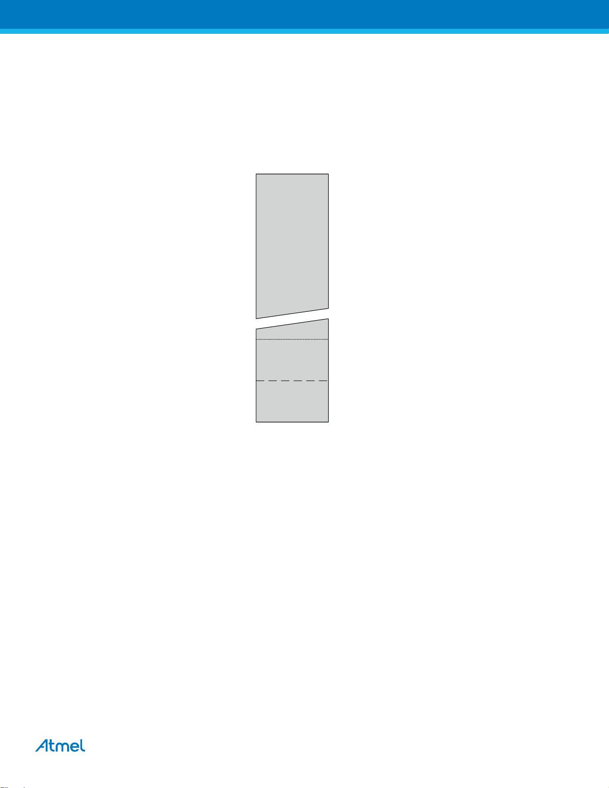
Figure 4-1. Flash memory sections.
0x000000
Application Flash
Section
4.3.1 Application Section
The Application section is the section of the flash that is used for storing the executable application code. The protection
level for the application section can be selected by the boot lock bits for this section. The application section can not store
any boot loader code since the SPM instruction cannot be executed from the application section.
4.3.2 Application Table Section
The application table section is a part of the application section of the flash memory that can be used for storing data.
The size is identical to the boot loader section. The protection level for the application table section can be selected by
the boot lock bits for this section. The possibilities for different protection levels on the application section and the
application table section enable safe parameter storage in the program memory. If this section is not used for data,
application code can reside here.
4.3.3 Boot Loader Section
While the application section is used for storing the application code, the boot loader software must be located in the boot
loader section because the SPM instruction can only initiate programming when executing from this section. The SPM
instruction can access the entire flash, including the boot loader section itself. The protection level for the boot loader
section can be selected by the boot loader lock bits. If this section is not used for boot loader software, application code
can be stored here.
Application Table
Flash Section
End Application
Start Boot Loader
Boot Loader Flash
Section
Flashend
XMEGA B [DATASHEET]
8291B–AVR–01/2013
21

4.3.4 Production Signature Row
The production signature row is a separate memory section for factory programmed data. It contains calibration data for
functions such as oscillators and analog modules. Some of the calibration values will be automatically loaded to the
corresponding module or peripheral unit during reset. Other values must be loaded from the signature row and written to
the corresponding peripheral registers from software. For details on calibration conditions such as temperature, voltage
references, etc., refer to the device datasheet.
The production signature row also contains an ID that identifies each microcontroller device type and a serial number for
each manufactured device. The serial number consists of the production lot number, wafer number, and wafer
coordinates for the device.
The production signature row cannot be written or erased, but it can be read from application software and external
programmers.
For accessing the production signature row, refer to “NVM Flash Commands” on page 382.
4.3.5 User Signature Row
The user signature row is a separate memory section that is fully accessible (read and write) from application software
and external programmers. It is one flash page in size, and is meant for static user parameter storage, such as calibration
data, custom serial number, identification numbers, random number seeds, etc. This section is not erased by chip erase
commands that erase the flash, and requires a dedicated erase command. This ensures parameter storage during
multiple program/erase operations and on-chip debug sessions.
4.4 Fuses and Lockbits
The fuses are used to configure important system functions, and can only be written from an external programmer. The
application software can read the fuses. The fuses are used to configure reset sources such as brownout detector and
watchdog, startup configuration, JTAG enable, and JTAG user ID.
The lock bits are used to set protection levels for the different flash sections (i.e., if read and/or write access should be
blocked). Lock bits can be written by external programmers and application software, but only to stricter protection levels.
Chip erase is the only way to erase the lock bits. To ensure that flash contents are protected even during chip erase, the
lock bits are erased after the rest of the flash memory has been erased.
An unprogrammed fuse or lock bit will have the value one, while a programmed fuse or lock bit will have the value zero.
Both fuses and lock bits are reprogrammable like the flash program memory.
4.5 Data Memory
The data memory contains the I/O memory, internal SRAM and optionally memory mapped EEPROM. The data memory
is organized as one continuous memory section, as shown in Figure 4-2 on page 23.
XMEGA B [DATASHEET]
8291B–AVR–01/2013
22
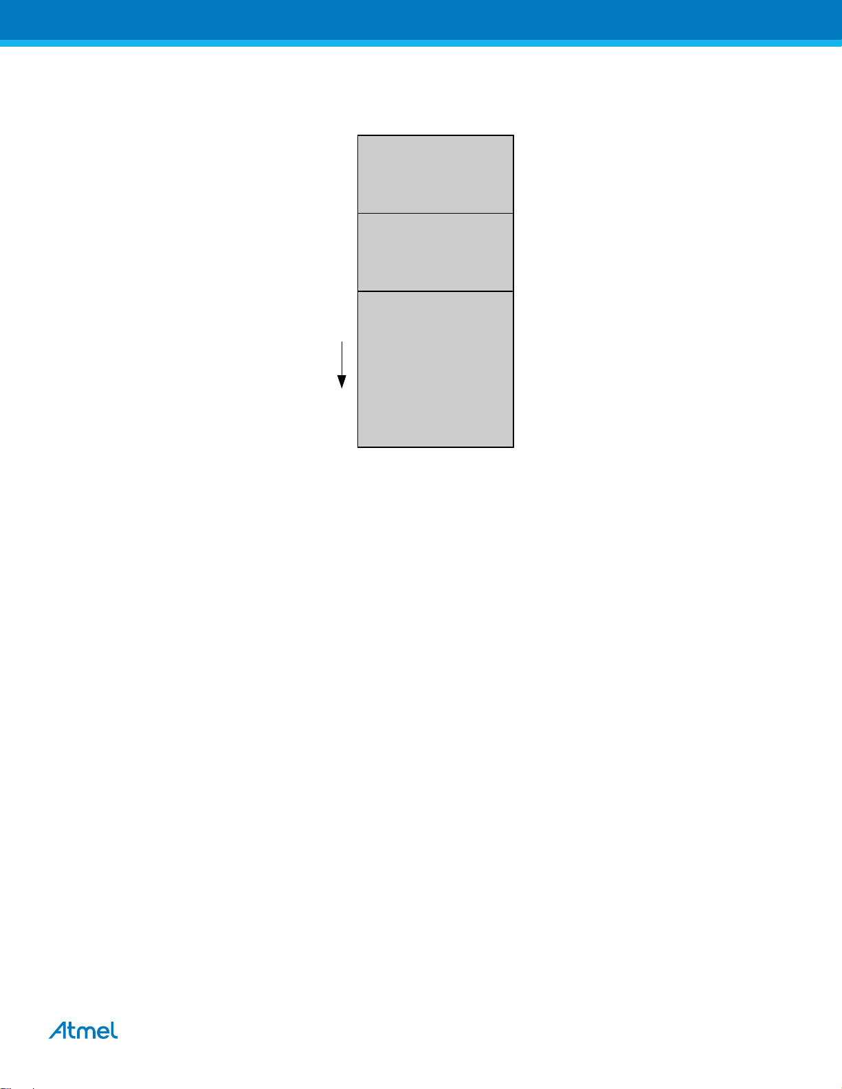
Figure 4-2. Data memory map.
Start/End Address Data Memory
0x0000
I/O Memory
(Up to 4 KB)
0x1000
EEPROM
(Up to 4 KB)
0x2000
Internal SRAM
(Up to 8 KB)
I/O memory, EEPROM, and SRAM will always have the same start addresses for all XMEGA devices.
4.6 Internal SRAM
The internal SRAM always starts at hexadecimal address 0x2000. SRAM is accessed by the CPU using the load
(LD/LDS/LDD) and store (ST/STS/STD) instructions.
4.7 EEPROM
XMEGA devices have EEPROM for nonvolatile data storage. It is either addressable in a separate data space (default)
or memory mapped and accessed in normal data space. The EEPROM supports both byte and page access. Memory
mapped EEPROM allows highly efficient EEPROM reading and EEPROM buffer loading. When doing this, EEPROM is
accessible using load and store instructions. Memory mapped EEPROM will always start at hexadecimal address
0x1000.
4.8 I/O Memory
The status and configuration registers for peripherals and modules, including the CPU, are addressable through I/O
memory locations. All I/O locations can be accessed by the load (LD/LDS/LDD) and store (ST/STS/STD) instructions,
which are used to transfer data between the 32 registers in the register file and the I/O memory. The IN and OUT
instructions can address I/O memory locations in the range of 0x00 to 0x3F directly. In the address range 0x00 - 0x1F,
single-cycle instructions for manipulation and checking of individual bits are available.
4.8.1 General Purpose I/O Registers
The lowest 4 I/O memory addresses are reserved as general purpose I/O registers. These registers can be used for
storing global variables and flags, as they are directly bit-accessible using the SBI, CBI, SBIS, and SBIC instructions.
4.9 Data Memory and Bus Arbitration
Since the data memory is organized as four separate sets of memories, the different bus masters (CPU, DMA controller
read and DMA controller write, etc.) can access different memories at the same time. As Figure 4-3 on page 24 shows,
XMEGA B [DATASHEET]
8291B–AVR–01/2013
23
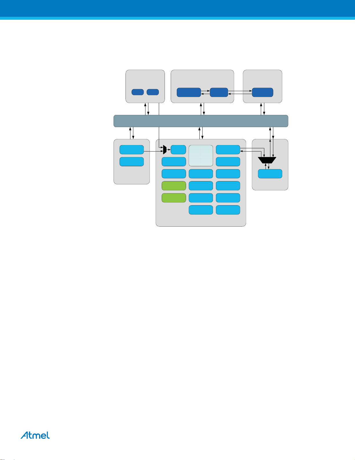
the CPU can access the EEPROM memory while the DMA controller is transferring data from internal SRAM to I/O
memory. The USB module acts as a bus master, and is connected directly to internal SRAM through a pseudo-dual-port
(PDP) interface.
Figure 4-3. Bus access.
4.9.1 Bus Priority
DMA
CH0 CH1
Flash
EEPROM
Non-Volatile
Memory
CPU
AVR core
OCD
Bus matrix
CRC
Crypto
Modules
Power
Management
AC
ADC
LCD
Event
System
USART
SPI
TWI
USB
Interrupt
Controller
Oscillator
Control
Timer /
Counter
Real Time
Counter
I/O
Peripherals and system modules
External
Programming
PDI
SRAM
RAM
When several masters request access to the same bus, the bus priority is in the following order (from higher to lower
priority):
1. Bus Master with ongoing access.
2. Bus Master with ongoing burst.
1. Alternating DMA controller read and DMA controller write when they access the same data memory section.
3. Bus Master requesting burst access.
1. CPU has priority.
4. Bus Master requesting bus access.
1. CPU has priority.
4.10 Memory Timing
Read and write access to the I/O memory takes one CPU clock cycle. A write to SRAM takes one cycle, and a read from
SRAM takes two cycles. For burst read (DMA), new data are available every cycle. EEPROM page load (write) takes one
cycle, and three cycles are required for read. For burst read, new data are available every second cycle. Refer to the
instruction summary for more details on instructions and instruction timing.
4.11 Device ID and Revision
Each device has a three-byte device ID. This ID identifies Atmel as the manufacturer of the device and the device type. A
separate register contains the revision number of the device.
XMEGA B [DATASHEET]
8291B–AVR–01/2013
24

4.12 JTAG Disable
It is possible to disable the JTAG interface from the application software. This will prevent all external JTAG access to the
device until the next device reset or until JTAG is enabled again from the application software. As long as JTAG is
disabled, the I/O pins required for JTAG can be used as normal I/O pins.
4.13 I/O Memory Protection
Some features in the device are regarded as critical for safety in some applications. Due to this, it is possible to lock the
I/O register related to the clock system, the event system, and the advanced waveform extensions. As long as the lock is
enabled, all related I/O registers are locked and they can not be written from the application software. The lock registers
themselves are protected by the configuration change protection mechanism. For details, refer to “Configuration Change
Protection” on page 14.
XMEGA B [DATASHEET]
8291B–AVR–01/2013
25

4.14 Register Description – NVM Controller
4.14.1 ADDR0 – Address register 0
The ADDR0, ADDR1, and ADDR2 registers represent the 24-bit value, ADDR. This is used for addressing all NVM
sections for read, write, and CRC operations.
Bit 76543210
+0x00 ADDR[7:0]
Read/Write R/W R/W R/W R/W R/W R/W R/W R/W
Initial Value 0 0 0 0 0 0 0 0
Bit 7:0 – ADDR[7:0]: Register Byte 0
This register gives the address low byte when accessing NVM locations.
4.14.2 ADDR1 – Address register 1
Bit 76543210
+0x01 ADDR[15:8]
Read/Write R/W R/W R/W R/W R/W R/W R/W R/W
Initial Value 0 0 0 0 0 0 0 0
Bit 7:0 – ADDR[15:8]: Address Register Byte 1
This register gives the address high byte when accessing NVM locations.
4.14.3 ADDR2 – Address register 2
Bit 76543210
+0x02 ADDR[23:16]
Read/Write R/W R/W R/W R/W R/W R/W R/W R/W
Initial Value 0 0 0 0 0 0 0 0
Bit 7:0 – ADDR[23:16]: Address Register Byte 2
This register gives the address extended byte when accessing NVM locations.
4.14.4 DATA0 – Data register 0
The DATA0, DATA1, and DATA registers represent the 24-bit value, DATA. This holds data during NVM read, write, and
CRC access.
Bit 76543210
+0x04 DATA[7:0]
Read/Write R/W R/W R/W R/W R/W R/W R/W R/W
Initial Value 0 0 0 0 0 0 0 0
Bit 7:0 – DATA[7:0]: Data Register Byte 0
This register gives the data value byte 0 when accessing NVM locations.
XMEGA B [DATASHEET]
8291B–AVR–01/2013
26
4.14.5 DATA1 – Data register 1
Bit 76543210
+0x05 DATA[15:8]
Read/Write R/W R/W R/W R/W R/W R/W R/W R/W
Initial Value 0 0 0 0 0 0 0 0
Bit 7:0 – DATA[15:8]: Data Register Byte 1
This register gives the data value byte 1 when accessing NVM locations.
4.14.6 DATA2 – Data register 2
Bit 76543210
+0x06 DATA[23:16]
Read/Write R/W R/W R/W R/W R/W R/W R/W R/W
Initial Value 0 0 0 0 0 0 0 0
Bit 7:0 – DATA[23:16]: Data Register Byte 2
This register gives the data value byte 2 when accessing NVM locations.
4.14.7 CMD – Command register
Bit 76543210
+0x0A
Read/Write R R/W R/W R/W R/W R/W R/W R/W
Initial Value 0 0 0 0 0 0 0 0
– CMD[6:0]
Bit 7 – Reserved
This bit is unused and reserved for future use. For compatibility with future devices, always write this bit to zero when this
register is written.
Bit 6:0 -CMD[6:0]: Command
These bits define the programming commands for the flash. Bit 6 is only set for external programming commands. See
“Memory Programming” on page 385” for programming commands.
4.14.8 CTRLA – Control register A
Bit 76543210
+0x0B
Read/Write RRRRRRRS
Initial Value 00000000
Bit 7:1 – Reserved
– – – – – – – CMDEX
These bits are unused and reserved for future use. For compatibility with future devices, always write these bits to zero
when this register is written.
Bit 0 – CMDEX: Command Execute
Setting this bit will execute the command in the CMD register. This bit is protected by the configuration change protection
(CCP) mechanism. Refer to “Configuration Change Protection” on page 14 for details on the CCP.
XMEGA B [DATASHEET]
8291B–AVR–01/2013
27

4.14.9 CTRLB – Control register B
Bit 7 6 5 4 3 2 1 0
+0x0C
Read/Write R R R R R/W R/W R/W R/W
Initial Value 0 0 0 0 0 0 0 0
Bit 7:4 – Reserved
– – – – EEMAPEN FPRM EPRM SPMLOCK
These bits are unused and reserved for future use. For compatibility with future devices, always write these bits to zero
when this register is written.
Bit 3 – EEMAPEN: EEPROM Data Memory Mapping Enable
Setting this bit enables data memory mapping of the EEPROM section. The EEPROM can then be accessed using load
and store instructions.
Bit 2 – FPRM: Flash Power Reduction Mode
Setting this bit enables power saving for the flash memory. If code is running from the application section, the boot loader
section will be turned off, and vice versa. If access to the section that is turned off is required, the CPU will be halted for
a time equal to the start-up time from the idle sleep mode.
Bit 1 – EPRM: EEPROM Power Reduction Mode
Setting this bit enables power saving for the EEPROM. The EEPROM will then be turned off in a manner equivalent to
entering sleep mode. If access is required, the bus master will be halted for a time equal to the start-up time from idle
sleep mode.
Bit 0 – SPMLOCK: SPM Locked
This bit can be written to prevent all further self-programming. The bit is cleared at reset, and cannot be cleared from
software. This bit is protected by the configuration change protection (CCP) mechanism.Refer to “Configuration Change
Protection” on page 14 for details on the CCP.
4.14.10 INTCTRL – Interrupt Control register
Bit 76543210
+0x0D
Read/Write R R R R R/W R/W R/W R/W
Initial Value 0 0 0 0 0 0 0 0
Bit 7:4 – Reserved
– – – – SPMLVL[1:0] EELVL[1:0]
These bits are unused and reserved for future use. For compatibility with future devices, always write these bits to zero
when this register is written.
Bit 3:2 – SPMLVL[1:0]: SPM Ready Interrupt Level
These bits enable the interrupt and select the interrupt level, as described in “Interrupts and Programmable Multilevel
Interrupt Controller” on page 121. This is a level interrupt that will be triggered only when the NVMBUSY flag in the
STATUS register is set to zero. Thus, the interrupt should not be enabled before triggering an NVM command, as the
NVMBUSY flag will not be set before the NVM command is triggered. The interrupt should be disabled in the interrupt
handler.
Bit 1:0 – EELVL[1:0]: EEPROM Ready Interrupt Level
These bits enable the EEPROM ready interrupt and select the interrupt level, as described in “Interrupts and
Programmable Multilevel Interrupt Controller” on page 121. This is a level interrupt that will be triggered only when the
NVMBUSY flag in the STATUS register is set to zerozero. Thus, the interrupt should not be enabled before triggering an
NVM command, as the NVMBUSY flag won’t be set before the NVM command is triggered. The interrupt should be
disabled in the interrupt handler.
XMEGA B [DATASHEET]
8291B–AVR–01/2013
28

4.14.11 STATUS – Status register
Bit 7 6 5432 1 0
+0x04 NVMBUSY FBUSY
Read/Write R R R R R R R R
Initial Value 0 0 0 0 0 0 0 0
Bit 7 – NVMBUSY: Nonvolatile Memory Busy
The NVMBUSY flag indicates if the NVM (Flash, EEPROM, lock bit) is being programmed. Once an operation is started,
this flag is set and remains set until the operation is completed. The NVMBUSY flag is automatically cleared when the
operation is finished.
Bit 7 - NVMBUSY: Nonvolatile Memory Busy
Bit 6 – FBUSY: Flash Busy
The FBUSY flag indicates if a flash programming operation is initiated. Once an operation is started, the FBUSY flag is
set and the application section cannot be accessed. The FBUSY flag is automatically cleared when the operation is
finished.
Bit 5:2 – Reserved
These bits are unused and reserved for future use. For compatibility with future devices, always write these bits to zero
when this register is written.
Bit 1 – EELOAD: EEPROM Page Buffer Active Loading
The EELOAD flag indicates that the temporary EEPROM page buffer has been loaded with one or more data bytes. It
remains set until an EEPROM page write or a page buffer flush operation is executed. For more details, see “Flash and
EEPROM Programming Sequences” on page 388.
Bit 0 – FLOAD: Flash Page Buffer Active Loading
The FLOAD flag indicates that the temporary flash page buffer has been loaded with one or more data bytes. It remains
set until an application, boot page write, or page buffer flush operation is executed. For more details, see “Flash and
EEPROM Programming Sequences” on page 388.
– – – – EELOAD FLOAD
XMEGA B [DATASHEET]
8291B–AVR–01/2013
29

4.14.12 LOCKBITS – Lock Bits register
Bit 76543210
+0x07 BLBB[1:0] BLBA[1:0] BLBAT[1:0] LB[1:0]
Read/Write R R R R R R R R
Initial Value 1 1 1 1 1 1 1 1
This register is a mapping of the NVM lock bits into the I/O memory space, which enables direct read access from the
application software. Refer to “LOCKBITS – Lock Bits register” on page 34 for a description.
4.15 Register Descriptions – Fuses and Lock Bits
4.15.1 FUSEBYTE0 – Fuse Byte 0
Bit 7 6543210
+0x00 JTAGUID[7:0]
Read/Write R/W R/W R/W R/W R/W R/W R/W R/W
Initial Value 0 0 0 0 0 0 0 0
Bit 7 – JTAGUID[7:0]: JTAG USER ID
These fuses can be used to set the default JTAG user ID for the device. During reset, the JTAGUID fuse bits will be
loaded into the MCU JTAG user ID register.
4.15.2 FUSEBYTE1 – Fuse Byte1
Bit 7 6543210
+0x01 WDWPER[3:0] WDPER[3:0]
Read/Write R/W R/W R/W R/W R/W R/W R/W R/W
Initial Value 0 0 0 0 0 0 0 0
Bit 7:4 – WDWPER[3:0]: Watchdog Window Timeout Period
These fuse bits are used to set initial value of the closed window for the Watchdog Timer in Window Mode. During reset
these fuse bits are automatically written to the WPER bits Watchdog Window Mode Control Register, refer to “WINCTRL
– Window Mode Control register” on page 118 for details.
Bit 3:0 – WDPER[3:0]: Watchdog Timeout Period
These fuse bits are used to set the initial value of the watchdog timeout period. During reset, these fuse bits are
automatically written to the PER bits in the watchdog control register. .RRefer to “CTRL – Control register” on page 117
for details.
XMEGA B [DATASHEET]
8291B–AVR–01/2013
30
 Loading...