

Page 1
Triple Driver with Thermal Monitoring
Description
The triple-driver IC includes three non-inverted and
current-limited output stages with an open collector.
Common thermal shutdown protects the outputs against
critical junction temperatures. Each output can sink a
Features
Three input comparators with Schmitt-trigger
characteristic
current of 20 mA, parallel output operation is possible.
The digital inputs have Schmitt-trigger function with
pull-up resistors to 5 V.
ESD protection acording to human body model:
2000 V (C = 100 pF, R = 1.5 k)
U6803B
Input clamping current capability of10 mA
Integrated protection cells (EMC, ESD, RF)
dedicated to all input stages
Common shutdown by junction-temperature monitor
Reset with hysteresis at low voltage
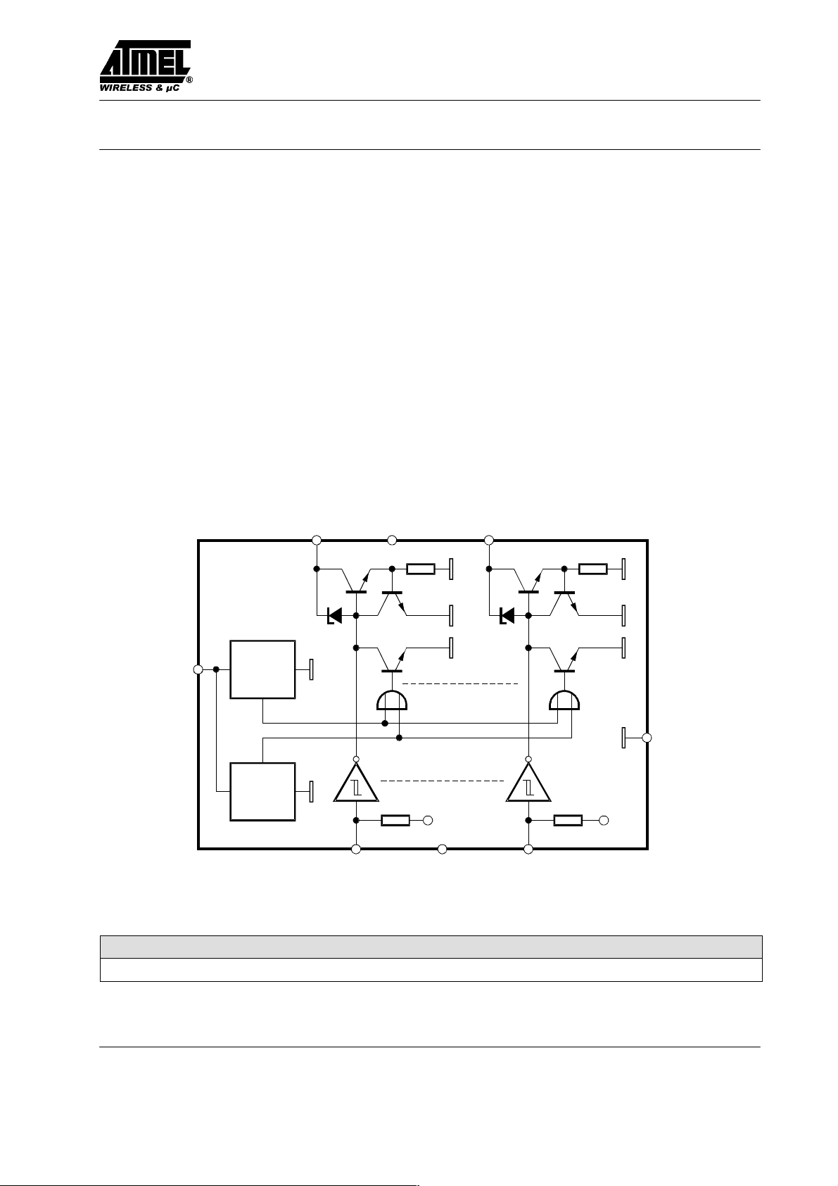
Block Diagram / Applications
V
O1
1 3
7
V
S
Thermal
shutdown
Under-
voltage
detection
V
O2
856
V
I1
Output stages:
– Short-circuit protected
– Load-dump protected @ 1 k
– No crosstalk on adjacent channels
– Jump start possible
V
O3
4
VS=5 V
V
I2
V
I3
V
S
13332
2
GND
Figure 1. Block diagram
Ordering Information
Extended Type Number Package Remarks
U6803B–FP SO8
Rev. A6, 28-Mar-01 1 (6)
Page 2

U6803B
Pin Description
V
O1
GND
V
V
O2
O3
1
2
3
4
13330
Figure 2. Pinning
V
8
I1
V
7
S
V
6
I2
V
5
I3
Basic Circuitry
The integrated circuit U6803B requires a stabilized
supply voltage (VS = 5 V5%) to comply with its
electrical characteristics. An external buffer capacitor of
C = 100 nF value is recommended. An integrated 14-V
Zener diode between VS and ground protects the supply
pin.
All input stages are provided with an integrated 250-k
pull-up resistor and can be directly connected to a
microcontroller.
All output stages are open collectors – each capable of
sinking 20 mA. Recommended external components:
Pin Symbol Function
1 V
O1
Output 1
2 GND Ground
3 V
4 V
5 V
6 V
7 V
8 V
O2
O3
I3
I2
I1
Output 2
Output 3
Input 3
Input 2
Supply voltage 5 V
S
Input 1
Current Limitation of the Output Stages
and Overtemperature Shut-down
A temperature-dependent current limitation in the range
of 25 to 100 mA protects the stages in case of a short.
Additionally, the chip temperature is monitored. For T
chip
> 148C, all outputs are disabled and automatically
enabled with a hysteresis of T
Chip
> 5C.
Transients and Load Dump
Pull-up resistor, R = 1 k
Capacitor to GND, C = 470 pF, see figure 3
Functional Description
General
ON state: Low level at the input stage activates the
corresponding output stage.
OFF state: The internal pull-up resistor provides high
level to the input comparator and deactivates the output
stage.
7-V Zener diodes between each input pin and GND are
capable of 10 mA clamping currents without crosstalk
on adjacent input stages.
A total clamping current of 30 mA should be observed
with respect to the power dissipation.
An integrated 28-V Zener diode protects each output
stage against transients and load-dump (Schaffner
pulses). With the help of external 1-k resistor, the output
transistor is capable to handle the corresponding current
which flows during each of these conditions. Apart from
that, the outputs are short circuit and overload protected.
Low-Voltage Detection
When the supply voltage is switched on, a power-on reset
pulse is generated internally which disables all output
stages until a defined supply-voltage level is reached. The
low-voltage detection is provided with a hysteresis of
V
= 0.5 V typically.
hyst
Rev. A6, 28-Mar-012 (6)
Page 3

U6803B
VS=5 V
100 nF
V
I1
V
Micro–
controller
I2
U6803B
V
I3
Figure 3. Application schematic
Absolute Maximum Ratings
Parameters Symbol Value Unit
Supply voltage V
Ambient temperature range T
Storage temperature range T
Maximum junction temperature T
V
Batt
Load
RRR
V
O1
V
O2
V
O3
C C C
S
amb
stg
j
Ω
3x 1k
3x 470 pF
13333
7.0 V
–40 to +125 C
–50 to +150 C
+150 C
Thermal Resistance
Parameters Symbol Value Unit
Junction ambient R
thJA
Rev. A6, 28-Mar-01 3 (6)
160 K/W
Page 4

U6803B
Electrical Characteristics
VS = 5 V5%, T
= 27C, reference point pin 2 (GND), unless otherwise specified, see figures 1 and 3.
amb
Parameters Test Conditions / Pins Symbol Min. Typ. Max. Unit
Supply Pin 7
Supply voltage V
Supply current Inputs open
Inputs closed to GND
Low-voltage detection
threshold:
ON
OFF
V
V
Low-voltage hysteresis V
Temperature shutdown T
Temperature shutdown
hysteresis
Input Pins 5, 6, 8
Zener-diode protection
I
= 10 mA V
I
voltage
Zener-diode clamping
current
Pull-up resistor R
Switching threshold OFF
ON
Hysteresis V
S
I
S
I
S
TH(ON)
TH(OFF)
hyst
Chip
T
hyst
I
I
I
I
V
I
V
I
hyst
4.75 5.25 V
0.8
7
3.7
3.0
3.2
13
4.6
3.8
mA
mA
0.55 1.05 V
140 149 C
5 C
6.7 8.5 V
10 mA
170 250 305 k
3.3
1.8
1.5 V
V
V
V
V
Output Pins 1, 3, 4
Zener-diode protection
I
= 10 mA V
O
O
26.5 V
voltage
Integrated capacitor 5 pF
Leakage current I
Saturation voltage (I
= 20 mA) V
O
Current limitation I
Propagation delay (470 pF, 1 k, 20 V) t
Leak
Sat
limit
d
25 100 mA
2.5 A
0.7 V
5 s
Rev. A6, 28-Mar-014 (6)
Page 5

Package Information
Package SO8
Dimensions in mm
0.4
5.00
4.85
1.4
0.25
0.10
1.27
3.81
85
14
5.2
4.8
3.7
3.8
6.15
5.85
technical drawings
according to DIN
specifications
U6803B
0.2
13034
Rev. A6, 28-Mar-01 5 (6)
Page 6

U6803B
Ozone Depleting Substances Policy Statement
It is the policy of Atmel Germany GmbH to
1. Meet all present and future national and international statutory requirements.
2. Regularly and continuously improve the performance of our products, processes, distribution and operating systems
with respect to their impact on the health and safety of our employees and the public, as well as their impact on
the environment.
It is particular concern to control or eliminate releases of those substances into the atmosphere which are known as
ozone depleting substances (ODSs).
The Montreal Protocol (1987) and its London Amendments (1990) intend to severely restrict the use of ODSs and forbid
their use within the next ten years. Various national and international initiatives are pressing for an earlier ban on these
substances.
Atmel Germany GmbH has been able to use its policy of continuous improvements to eliminate the use of ODSs listed
in the following documents.
1. Annex A, B and list of transitional substances of the Montreal Protocol and the London Amendments respectively
2. Class I and II ozone depleting substances in the Clean Air Act Amendments of 1990 by the Environmental
Protection Agency (EPA) in the USA
3. Council Decision 88/540/EEC and 91/690/EEC Annex A, B and C (transitional substances) respectively.
Atmel Germany GmbH can certify that our semiconductors are not manufactured with ozone depleting substances
and do not contain such substances.
We reserve the right to make changes to improve technical design and may do so without further notice.
Parameters can vary in different applications. All operating parameters must be validated for each customer
application by the customer. Should the buyer use Atmel Wireless & Microcontrollers products for any unintended
or unauthorized application, the buyer shall indemnify Atmel Wireless & Microcontrollers against all claims,
costs, damages, and expenses, arising out of, directly or indirectly, any claim of personal damage, injury or death
associated with such unintended or unauthorized use.
Data sheets can also be retrieved from the Internet: http://www.atmel–wm.com
Atmel Germany GmbH, P.O.B. 3535, D-74025 Heilbronn, Germany
Telephone: 49 (0)7131 67 2594, Fax number: 49 (0)7131 67 2423
Rev. A6, 28-Mar-016 (6)
 Loading...