


ATMEL U2510B-M Datasheet
All-Band AM/FM Receiver and Audio Amplifier
Description
The U2510B is an integrated bipolar one-chip AM/FM
radio circuit. It contains an FM front end with
preamplifier, FM IF and demodulator, a complete AM
Features
Superior FM strong signal behavior by using RF AGC
receiver, an AF amplifier and a mode switch for AM, FM
and tape. This circuit is designed for clock radios and
portable radio-cassette recorders.
DC mode control: AM, FM and tape
U2510B
Soft mute and HCC for decreasing interstation noise
in FM mode
Excellent AFC performance (level controlled, both
polarities available)
Level indicator (LED drive) for AM and FM
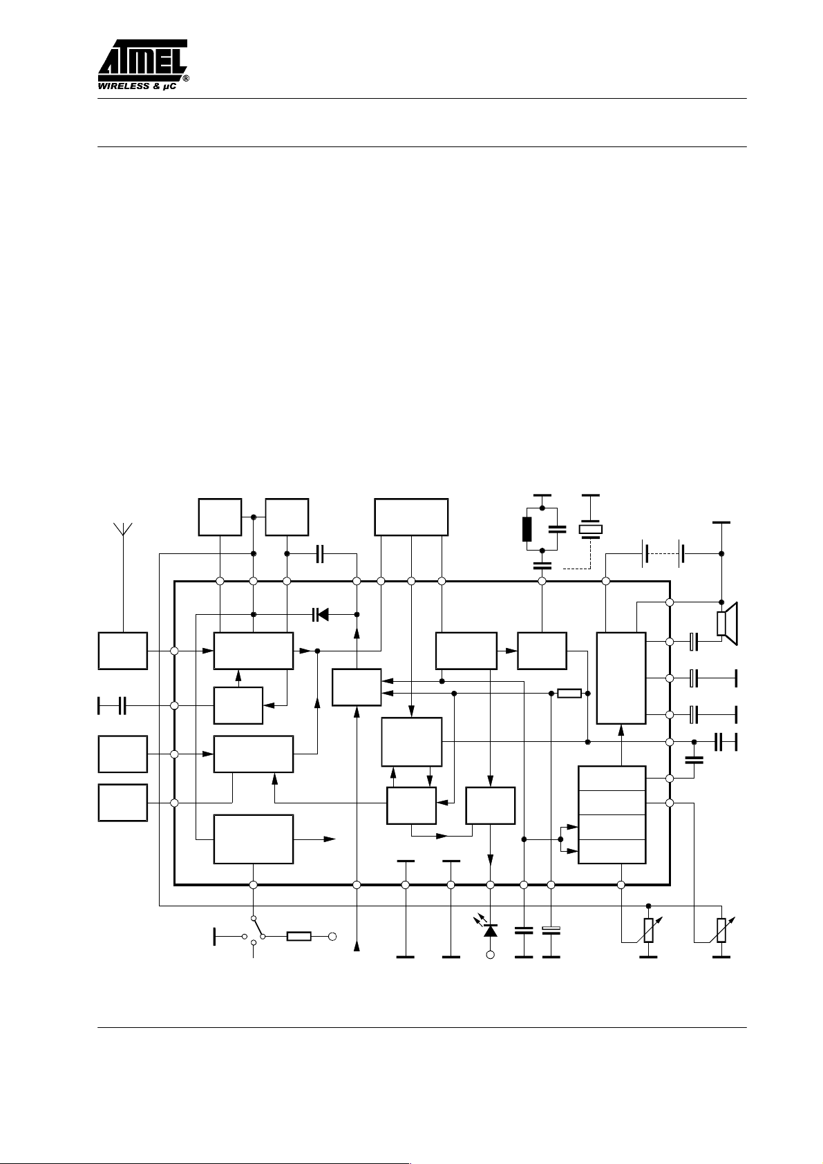
Block Diagram
FM osc.
tank
87 6
AFC
FM
front end
FM
AM
front end
RFAGC
AM/FM
and
15
IF BPE
14 16
AFC
control
AM IF
amp. and
detect.
IF
AGC
AGC
21 13 20 19 1
FM ant.
FM RF
BPE
AGC
AM
ant.
AM osc.
tank
12
11
10
5
V
Ref
FM RF
tank
9
AGC
Voltage stab.
mode control
Wide supply-voltage range and low quiescent current
High AF output power: 1 W
Electronic volume control
Electronic AF bandwidth control (treble and high cut)
Output stage for headphone and speaker drive
(Replaceable)
V
S
AM
IF
FM IF
amp.
Level
indic.
226
FM
discr.
22 18
Power
amp.
AF preamp.
Volume
Mute
HCC
28
27
3
25
23
24
4
S
AM
FM
2
Tape
V
S
AFC mode
Figure 1. Block diagram
LED
V
S
Treble Vol
13912
Rev. A3, 23-Feb-01 1 (15)

U2510B
Order Information
Extended Type Number Package Remarks
U2510B-M SDIP28
U2510B-M__T SDIP28 VS < 6 V supply voltage
Pin Description
Mute
FM-discr
Vol ctrl in
AMOsc
FM-AFC
FMOsc
V
FMtank
AMtank
FM-AGC
FMin
FE-GND
AM/FM
IFout
CF
Ref
1
2
3
4
5
6
7
8
9
10
11
12
13
14
14812
Figure 2. Pinning
Pin Symbol Function
1 Mute Mute voltage output, time constant (C23),
2 FM-discr FM discriminator filter connection, ceramic
3 CF Audio negative feedback input. Blocking
4 Vol ctrl in Input for volume control voltage
mute depth and threshold adjustable by load
resistance (R3)
resonator or equivalent LC-circuit
capacitor (C8) determines the audio amplifiers
low-end cut-off frequency
28
27
26
25
24
23
22
21
20
19
18
17
16
15
AF-GND
AFout
V
S
Ripple in
AFin
AM/FM detect
V
AGC/AFC
AFC switch
IF-GND
LED drive
V
Treble in
FM-IFin
AM-IFin
Mode ctrl
switch
Pin Symbol Function
5 AMOsc AM oscillator tank circuit input, recommended
6 FM–AFC AFC diode connection, coupling capacitor
7 FMOsc FM oscillator tank circuit input, recommended
8 V
9 FMtank FM RF tank circuit connection, recommended
10 AMtank AM RF tank circuit connection, recommended
11 FM-AGC FM AGC voltage output, time constant (C20).
12 FMin FM RF input (common-base preamplifier
13 FE-GND FM front-end ground
14 AM/FM
15 Mode ctrl
16 AM-IFin AM IF input, input impedance = 3.1 k
17 FM-IFin FM IF input, input impedance = 330
18 V
19 LED drive Level indicator output
20 IF-GND IF ground
21 AFC switch AFC function control input:
22 V
23 AM/FM
24 AFin Audio amplifier input, input resistance
25 Ripple in Ripple filter connection. Load capacitance
26 V
27 AFout Audio amplifier output
28 AF-GND Ground of the audio power stage
IFout
switch
Treble in
AGC/AFC
detect
load impedance approximately 2.5 k
(C19) determines the AFC characteristic
(holding range and slope)
load impedance approximately 3 k
Regulated voltage output (2.4 V)
Ref
load impedance approximately 3 k
load impedance approximately 20 k
Loading this pin by a resistor (to GND) will
increase the FM AGC threshold, grounding
this pin will switch off the FM AGC function
transistor), recommended (RF) source
impedance approximately 100
AM/FM IF output
(collector output of the IF preamplifier)
Mode control input:
Pin | Function
open | F M
Ground | AM
VS (R4 = 10 k) | Tape
Treble control voltage input
(open-collector output, LED drive)
Pin | Function
open | AFC off
Ground | f
V
S
AGC/AFC voltage, time constant adjust (C10),
input impedance approximately 42 k
AM/FM detector output, the load capacitor
(C11) in conjunction with the detector output
resistance (7.5 k) determines the (FM)
deemphasis as well as the (modulation)
frequency response of the AM detector
approximately 100 k coupling capacitor
(C9) determines the low frequency response
(C12) determines the frequency response of the
supply-voltage ripple rejection
Supply voltage input
S
| f
OSC
OSC
> f
in
< f
in
Rev. A3, 23-Feb-012 (15)

Terminal Voltages
Test circuit: Vin = 0
Pin Symbol
1 Mute voltage (R3 = 0) V
2 FM discriminator V
3 Negative feedback V
4 Volume control input (S4 = A) V
5 AM oscillator V
6 FM AFC V
7 FM oscillator V
8 V
Ref
9 FM RF tank V
10 AM input V
11 FM AGC V
12 FM input V
13 Front end ground V
14 AM/FM IF output V
15 Mode control switch V
16 AM IF input V
17 FM IF input V
18 Treble control input (S5 = A) V
19 LED V
20 IF ground V
21 AFC switch (S3 = off) V
22 AGC (AM)/AFC (FM) V
23 Detector output V
24 AF input V
25 Ripple filter V
26 Supply voltage V
27 AF output V
28 AF ground V
U2510B
Voltage/V
VS = 3 V VS = 6 V
AM FM TAPE AM FM TAPE
1
2
3
4
5
6
7
V
8
9
10
11
12
13
14
15
16
17
18
19
20
21
22
23
24
25
26
27
28
– 1.6 – – 1.6 –
– 1.0 – – 1.0 –
1.2 1.2 1.2 2.6 2.6 2.6
2.4 2.4 2.4 2.4 2.4 2.4
2.4 – – 2.4 – –
– 1.9 – – 1.9 –
– 2.4 – – 2.4 –
2.4 2.4 2.4 2.4 2.4 2.4
– 2.4 2.4 – 2.4 –
2.4 – – – 2.4 –
– 0 – – 0 –
1.4 – – 1.4 –
– – – – – –
2.9 2.7 – 5.9 5.7 –
0 – 2.9 0 – 5.7
0 – – 0 – –
– 0.7 – – 0.7 –
2.4 2.4 2.4 2.4 2.4 2.4
0 0 0 0 0 0
1.2 1.2 1.2 1.2 1.2 1.2
1.5 1.2 – 1.5 1.2 –
1.5 1.2 – 1.5 1.2 –
1.5 1.5 1.5 1.5 1.5 1.5
2.7 2.7 2.7 5.3 5.3 5.3
3.0 3.0 3.0 6.0 6.0 6.0
1.2 1.2 1.2 2.6 2.6 2.6
0 0 0 0 0 0
Rev. A3, 23-Feb-01 3 (15)

U2510B
Absolute Maximum Ratings
Parameters Symbol Value Unit
Supply voltage V
Power dissipation P
Ambient temperature range T
Electrical Characteristics
S
tot
amb
13 V
900 mW
–20 to +75 °C
VS = 6 V, T
= 25°C, test circuit (figure 16), unless otherwise specified
amb
Parameters Test Conditions / Pins Symbol Min. Typ. Max. Unit
Supply voltage range V
Oscillator stop voltage V
S
S
2.5 9 * V
2.2 V
Operating temperature range T –20 +75 °C
Supply quiescent current Vi1 = Vi2 = V4 = 0;
AM (S2 = AM)
FM (S2 = FM)
TAPE (S2 = Tape)
Regulated voltage Pin 8 V
I
I
I
Ref
S
S
S
4.0
6.5
2.2
2.4 V
Audio amplifier Vi3 (Pin 24), test point: Vo (Pin 27) f = 1 kHz
AF measuring range: 30 Hz to 20 kHz, S2 = Tape, S4 = A, S5 = A
Input resistance Pin 24 R
Closed loop voltage gain GV
= 20 log (Vo/Vi3)
af1
Vi3 = 10 mV GV
Output voltage Vi3 = 100 mV, S4 = B V
High–end cut-off frequency fc (–3 dB)
S5 = B
Supply-voltage rejection ratio SVRR = 20 log (V
V
= 200 mV,
hum
f
= 200 Hz, S4 = B SVRR 32 dB
hum
hum/Vo
)
Noise voltage S4 = B, Vi3 = 0 V
j
af1
o
f
c
f
c
n
100 k
40 dB
0.7 3 mV
13
0.8
kHz
kHz
300 1000 V
AF output power THD = 10 %, RL = 8
VS = 4.5 V
VS = 6.0 V
VS = 9.0 V
P
o
P
o
P
o
400
225
420
1000
mW
mW
mW
Distortion Po = 50 mW, RL = 8 d 0.6 %
FM section, Vi2 = 60 dBV, fi2 = 98 MHz, fm = 1 kHz, dev. = 22.5 kHz, f
= 10.7 MHz,
iIF
AF measuring range: 300 Hz to 20 kHz, S2 = FM, S1 = A, S6 = B, test point: VD (Pin 23)
FM front-end voltage gain GVFM = 20 log (V
S1 = B, Vi2 = 40 dbV GV
Recovered audio voltage Pin 23 VD
Detector output resistance Pin 23 R
iIF
/ Vi2)
Do
FM
30 dB
af
85 mV
7.5 k
Detector output distortion dev. = 75 kHz
Vi2 = 60 dBV
Vi2 = 105 dBV
THD
THD
0.5
0.8
* U2510B-M__T: max. 6 V
mA
mA
mA
%
%
Rev. A3, 23-Feb-014 (15)

Electrical Characteristics (continued)
U2510B
VS = 6 V, T
= 25°C, test circuit (figure 16), unless otherwise specified
amb
Parameters Test Conditions / Pins Symbol Min. Typ. Max. Unit
AM rejection ratio m = 30% AM
RF sensitivity (S+N)/N = 26 dB
(S+N)/N = 46 dB
Limiting threshold (-3 dB) V
RR
V
i2
V
i2
i2
Mute voltage Test point: Mute
Vi2 = 0
Vi2 = 60 dBV
V
V
mute
mute
Mute depth Referred to V0 at Vi2 = 0
S6 = A
S6 = C
AFC holding range f
> fin, S3 = A, S6 = A
OSC
V
10 dBV
i2
Vi2 = 20 dBV
Vi2 = 80 dBV
LED current I
Oscillator voltage eZ
= 2.5 k Pin 7 V
load
AM section Vi1 = 60 dBV, fi1 = 1.6 MHz, fm = 1 kHz, m = 30%, f
MD
MD
FHR
FHR
FHR
LED
OSC
= 455 kHz,
iIF
AF measuring range: 300 Hz to 20 kHz, (S2 = AM, S1 = B, test point: VD)
AM front end voltage gain GVAM = 20 log (V
iIF/Vi1
)
GV
AM
Vi1 = 20 dBV, S1 = A
Recovered audio voltage V
Detector output resistance Pin 23 R
Detector output distortion Vi1 = 60 dBV
Vi1 = 105 dBV
RF sensitivity (S+N)/N= 10 dB
(S+N)/N= 26 dB
(S+N)/N= 46 dB
AGC figure of merit referred
to V
D af
Vi1 = 105 dBV, voltage
drop (V
) = –10 dB FOM 100 dB
D af
IF input resistance Pin 16 Z
LED current I
Oscillator voltage Pin 5 V
D af1
Do
THD
THD
V
i1
V
i1
V
i1
i
LED
OSC
25 dB
9
22
3 dBV
1.8
0.4
26
20
no AFC
180
220
5.5 mA
180 mV
25 dB
70 mV
7.5 k
1
3
0
16
35
3.1 k
5.5 mA
160 mV
dBV
dBV
V
V
dB
dB
kHz
kHz
%
%
dBV
dBV
dBV
Rev. A3, 23-Feb-01 5 (15)