

Page 1
Features
•
Carrier Frequency f
•
Typical Data Rate up to 5 kbaud at 125 kHz
•
Suitable for Manchester and Bi-phase Modulation
•
Power Supply from the Car Battery or from 5-V Regulated Voltage
•
Optimized for Car Immobilizer Applications
•
Tuning Capability
•
Microcontroller-compatible Interface
•
Low Power Consumption in Standby Mode
•
Power-supply Output for Microcontroller
100 kHz to 150 kHz
osc
Read/Write
Base Station
Applications
•
Car Immobilizers
•
Animal Identification
•
Access Control
•
Process Control
1. Description
The U2270B is an IC for IDIC® read/write base stations in contactless identification
and immobilizer systems.
The IC incorporates the energy-transfer circuit to supply the transponder. It consists of
an on-chip power supply, an oscillator and a coil driver optimized for automotive-specific distances. It also includes all signal-processing circuits which are necessary to
transform the small input signal into a microcontroller-compatible signal.
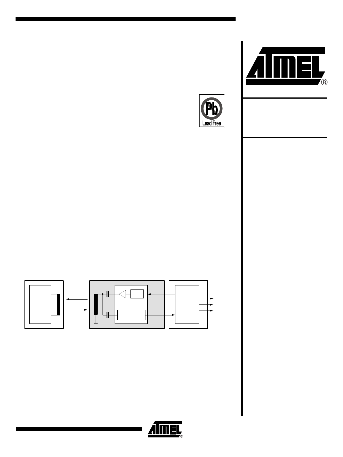
Figure 1-1. System Block Diagram
Transponder/TAG
Transponder
IC
RF field
typ. 125 kHz
Read/write base station
Osc
U2270B
NF read channel
Carrier
enable
Data
output
MCU
Unlock
System
U2270B
Rev. 4684B–RFID–09/05
Page 2
Figure 1-2. Block Diagram
COIL1
COIL2
DGND
Input
DV
Driver
Lowpass filter
V
S
EXT
= 1
Amplifier
Schmitt trigger
HIPASS OEGND
Power supply
&
V
S
V
Batt
Oscillator
Frequency
adjustment
Standby
MS
CFE
RF
Output
&
2
U2270B
4684B–RFID–09/05
Page 3

2. Pin Configuration
Figure 2-1. Pinning
Table 2-1. Pin Description
Pin Symbol Function
1 GND Ground
2 OUTPUT Data output
3 OE Data output enable
4 INPUT Data input
5 MS Mode select coil 1: common mode/differential mode
6 CFE Carrier frequency enable
7 DGND Driver ground
8 COIL2 Coil driver 2
9 COIL1 Coil driver 1
10 VEXT External power supply
11 DVS Driver supply voltage
12 VBatt Battery voltage
13 STANDBY Standby input
14 VS Internal power supply (5V)
15 RF Frequency adjustment
16 HIPASS DC decoupling
GND
OUTPUT
OE
INPUT
MS
CFE
DGND
COIL2
U2270B
1
16
HIPASS
2
15
RF
3
14
VS
4
13
STANDBY
5
12
VBATT
6
11
DVS
7
10
VEXT
8
9
COIL1
4684B–RFID–09/05
3
Page 4
3. Functional Description
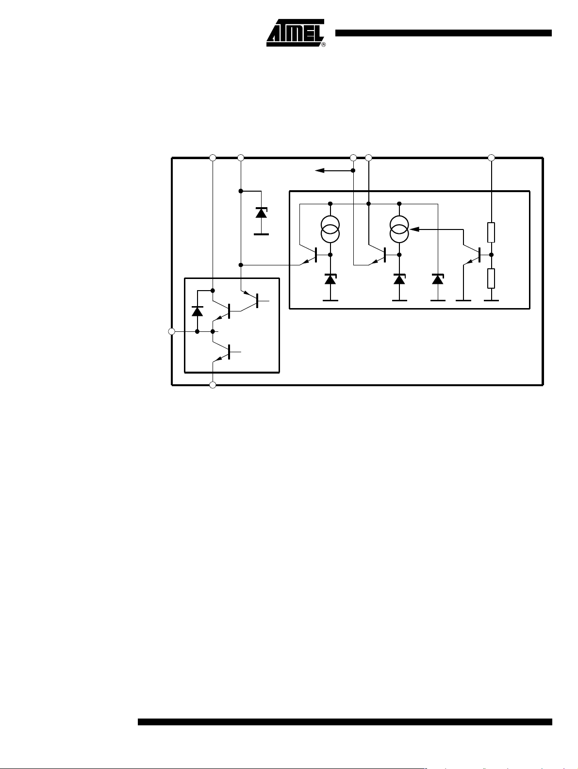
3.1 Power Supply (PS)
Figure 3-1. Equivalent Circuit of Power Supply and Antenna Driver
DV
S
V
EXT
internal supply
9 V
6 V 6 V 18 V
V
S
V
Batt
Standby
25 kΩ
12 kΩ
PS
COILx
DRV
DGND
The U2270B can be operated with one external supply voltage or with two externally-stabilized
supply voltages for an extended driver output voltage or from the 12-V battery voltage of a vehicle. The 12-V supply capability is achieved via the on-chip power supply (see Figure 3-1). The
power supply provides two different output voltages, V
V
is the internal power supply voltage except for the driver circuit. Pin VS is used to connect a
S
block capacitor. V
sumption is very low. V
can be switched off by Standby pin. In standby mode, the chip’s power con-
S
is the supply voltage of the antenna’s pre-driver. This voltage can
EXT
also be used to operate external circuits, like a microcontroller. In conjunction with an external
NPN transistor it also establishes the supply voltage of the antenna coil driver, DVS.
and V
S
EXT
.
4
U2270B
4684B–RFID–09/05
Page 5

3.2 Operation Modes to Power the U2270B
The following section explains the 3 different operation modes to power the U2270B.
3.2.1 One-rail Operation
All internal circuits are operated from one 5-V power rail (see Figure 3-2). In this case, V
and DVS serve as inputs. V
Figure 3-2. One Rail Operation Supply
is not used but should also be connected to that supply rail.
Batt
+5 V (stabilized)
U2270B
, V
S
EXT
3.2.2 Two-rail Operation
In this application, the driver voltage, D
higher voltage than the rest of the circuitry to obtain a higher driver-output swing and thus a
higher magnetic field (see Figure 3-3). V
ages can be as high as 8 V. This operation mode is intended to be used in situations where an
extended communication distance is required.
Figure 3-3. Two Rail Operation Supply
DVSV
DVSV
EXTVSVBatt
, and the pre-driver supply, V
VS
is connected to a 5-V supply, whereas the driver volt-
S
EXTVSVBatt
Standby
Standby
7 to 8 V (stabilized)
5 V (stabilized)
, are operated at a
EXT
3.2.3 Battery-voltage Operation
Using this operation mode, V
3-4). For this mode, an external voltage regulator is not needed. The IC can be switched off via
the Standby pin. V
a microcontroller (even in Standby mode).
Pin V
EXT
and V
4).The maximum current into the pins is determined by the maximum power dissipation and the
maximum junction temperature of the IC.
4684B–RFID–09/05
and V
S
supplies the base of an external NPN transistor and external circuits, like
EXT
are overvoltage protected via internal Zener diodes (see Figure 3-1 on page
Batt
are generated by the internal power supply (see Figure
EXT
5
Page 6

Figure 3-4. Battery Operation
7 to 16 V
DVSV
EXTVSVBatt
Standby
Table 3-1. Characteristics of the Various Operation Modes
Operation Mode External Components Required Supply-voltage Range
One-rail operation
Two-rail operation
1 Voltage regulator
1 Capacitor
2 Voltage regulators
2 Capacitors
5V ±10% ≈ 4V No
5V ±10%
7V to 8V
1 Transistor
2 Capacitors Optional for load
Battery-voltage operation
dump protection:
6V to 16V ≈ 4V Yes
1 Resistor
1 Capacitor
3.3 Oscillator (Osc)
The frequency of the on-chip oscillator is controlled by a current fed into the RF input. An integrated compensation circuit ensures a wide temperature range and a supply-voltageindependent frequency which is selected by a fixed resistor between R
For 125 kHz, a resistor value of 110 kΩ is defined. For other frequencies, use the following
formula:
14375
Ω[]
--------------------- 5–=
f0kHz
[]
Rtk
Driver Output
Standby Mode
Voltage Swing
6V to 7V No
(pin 15) and VS (pin 14).
F
Available
This input can be used to adjust the frequency close to the resonance of the antenna. For more
details refer to the section “Applications” on page 10” and to the application note ANT019.
Figure 3-5. Equivalent Circuit of Pin R
6
U2270B
F
2 kΩ
V
S
R
f
R
F
4684B–RFID–09/05
Page 7

3.4 Filter (LPF)
U2270B
The fully-integrated lowpass filter (4th-order butterworth) removes the remaining carrier signal
and high-frequency disturbances after demodulation. The upper cut-off frequency of the LPF
depends on the selected oscillator frequency. The typical value is f
rates up to f
/25 are possible if Bi-phase or Manchester encoding is used.
Osc
A highpass characteristic results from the capacitive coupling at the input pin 4 as shown in Fig-
ure 3-6. The input voltage swing is limited to 2 V
. For frequency response calculation, the
pp
impedances of the signal source and LPF input (typical 220 kΩ) have to be considered. The rec-
ommended values of the input capacitor for selected data rates are given in the section
“Applications”.
Note: After switching on the carrier, the DC voltage of the coupling capacitor changes rapidly. When the
antenna voltage is stable, the LPF needs approximately 2 ms to recover full sensitivity.
Figure 3-6. Equivalent Circuit of Pin Input
V
+ 0.4 V
Bias
/18. That means that data
Osc
3.5 Amplifier (AMP)
The differential amplifier has a fixed gain, typically 30. The HIPASS pin is used for dc decoupling. The lower cut-off frequency of the decoupling circuit can be calculated as follows:
f
The value of the internal resistor R
Recommended values of C
on page 10.
cut
--------------------------------------------=
2 π C
1
HPRi
R
S
Input
C
IN
V
10 kΩ
Bias
- 0.4 V
210 kΩ
V
Bias
×××
can be assumed to be 2.5 kΩ.
i
for selected data rates can be found in the section “Applications”
HP
4684B–RFID–09/05
7
Page 8

Figure 3-7. Equivalent Circuit of Pin HIPASS
R
R
LPF
V
Ref
+
Schmitt
trigger
3.6 Schmitt Trigger
R
HIPASS
R
i
R
C
HP
The signal is processed by a Schmitt trigger to suppress possible noise and to make the signal
microcontroller compatible. The hysteresis level is 100 mV symmetrically to the DC operation
point. The open-collector output is enabled by a low level at OE (pin 3).
Figure 3-8. Equivalent Circuit of Pin OE
7 µA
OE
8
U2270B
4684B–RFID–09/05
Page 9

3.7 Driver (DRV)
U2270B
The driver supplies the antenna coil with the appropriate energy. The circuit consists of two independent output stages. These output stages can be operated in two different modes. In common
mode, the outputs of the stages are in phase. In this mode, the outputs can be interconnected to
achieve a high-current output capability. Using the differential mode, the output voltages are in
anti-phase. Thus, the antenna coil is driven with a higher voltage. For a specific magnetic field,
the antenna coil impedance is higher for the differential mode. As a higher coil impedance
results in a better system sensitivity, the differential mode should be preferred.
The CFE input is intended to be used for writing data into a read/write or a crypto transponder.
This is achieved by interrupting the RF field with short gaps. The various functions are controlled
by the inputs MS and CFE (refer to the function table). The equivalent circuit of the driver is
shown in Figure 3-1 on page 4.
Figure 3-9. Equivalent Circuit of Pin MS
30 µA
MS
Figure 3-10. Equivalent Circuit of Pin CFE
CFE
30 µA
4684B–RFID–09/05
9
Page 10

3.8 Function Table
4. Applications
CFE MS COIL1 COIL2
Low Low High High
Low High Low High
High Low
High High
OE Output Standby U2270B
Low Enabled Low Standby mode
High Disabled High Active
To achieve the system performance, consider the power-supply environment and the magneticcoupling situation.
The selection of the appropriate power-supply operation mode depends on the quality of supply
voltage. If an unregulated supply voltage in the range of V = 7V to 16V is available, the internal
power supply of the U2270B can be used. In this case, standby mode can be used and an external low-current microcontroller can be supplied.
If a 5-V supply rail is available, it can be used to power the U2270B. In this case, please check
that the voltage is noise-free. An external power transistor is not necessary.
The application depends also on the magnetic-coupling situation. The coupling factor mainly
depends on the transmission distance and the antenna coils. The following table lists the appropriate application for a given coupling factor. The magnetic coupling factor can be determined
using Atmels test transponder coil.
Table 4-1. Magnetic Coupling
Magnetic Coupling Factor Appropriate Application
k > 3% Free-running oscillator
k > 1% Diode feedback
k > 0.5%
k > 0.3%
Diode feedback
plus frequency altering
Diode feedback
plus fine frequency tuning
The maximum transmission distance is also influenced by the accuracy of the antenna’s resonance. Therefore, the recommendations given above are proposals only. A good compromise
for the resonance accuracy of the antenna is a value in the range of f
= 125 kHz ±3%. Further
res
details concerning the adequate application and the antenna design is provided in the section
“Antenna Design Hints”.
10
U2270B
4684B–RFID–09/05
Page 11

U2270B
The application of the U2270B includes the two capacitors CIN and CHP whose values are linearly dependent on the transponder’s data rate. The following table gives the appropriate values
for the most common data rates. The values are valid for Manchester- and Bi-phase-code.
Table 4-2. Recommended Cap Values
Data Rate f = 125 kHz Input Capacitor (CIN) Decoupling Capacitor (CHP)
f/32 = 3.9 kbit/s 680 pF 100 nF
f/64 = 1.95 kbit/s 1.2 nF 220 nF
The following applications are typical examples. The values of C
transponder’s data rate only. The arrangement to fit the magnetic-coupling situation is also independent from other design issues except for one constellation. This constellation, consisting of
diode feedback plus fine frequency tuning together with the two-rail power supply, should be
used if the transmission distance of is d ≈ 10 cm.
4.1 Application 1
Application using few external components. This application is for intense magnetic coupling
only.
Figure 4-1. Application Circuit 1
5 V
47 nF
470 kΩ
1.5 nF
47 µF
1N4148
R
C
IN
1.35 mH
V
Batt
DV
S
INPUT
COIL1
V
EXTVS
U2270B
STANDBY
OUTPUT
110 kΩ
RF
MS
CFE
OE
HIPASS
and CHP correspond to the
IN
V
DD
Micro-
controller
H
C
P
4684B–RFID–09/05
1.2 nF
COIL2
DGND GND
V
SS
11
Page 12

4.2 Application 2
Basic application using diode feedback. This application allows higher communication distances
than application 1
Figure 4-2. Application Circuit 2
75 kΩ
100 kΩ
1.2 nF
1.35 mH
Antenna
1N4148
470 kΩ
4x
1N4148
82 Ω
1.5 nF
43 kΩ
68 kΩ
4.7 nF
C
C
HP
22 mF
22 mF
360 Ω
V
DD
Micro-
controller
V
SS
12 V
GND
BC639
22 µF
V
V
S
RF
COIL 2
EXT
DVSV
Batt
MS
CFE
U2270B
COIL 1
Input
IN
HIPASS
DGND GND
Standby
Output
OE
I/O
12
U2270B
4684B–RFID–09/05
Page 13

4.3 Application 3
This application is comparable to application 2 but alters the operating frequency. This allows
higher antenna resonance tolerances and/or higher communication distances. This application
is preferred if the detecting microcontroller is close to the U2270B as an additional microcontroller signal controls the adequate operating frequency.
Figure 4-3. Application Circuit 3
U2270B
75 kΩ
100 kΩ
1 nF
1.5 mH
Antenna
1N4148
180 pF
100 Ω
BC846
4x 1N4148
82 Ω
470 kΩ
1.5 kΩ
43 kΩ
1.5 nF
4.7 kΩ
68 kΩ
4.7 nF
C
IN
5 V
22 µF
V
S
RF
COIL 2
COIL 1
Input
HIPASS
C
HP
DGND GND
V
EXT
U2270B
DVSV
Standby
Output
Batt
MS
CFE
OE
V
DD
Micro-
controller
V
SS
47 nF
GND
4684B–RFID–09/05
Note: Application examples have not been examined for series use or reliability, and no worst case sce-
narios have been developed. Customers who adapt any of these proposals must carry out their
own testing and be convinced that no negative consequences arise from the proposals.
13
Page 14

5. Absolute Maximum Ratings
Stresses beyond those listed under “Absolute Maximum Ratings” may cause permanent damage to the device. This is a stress rating
only and functional operation of the device at these or any other conditions beyond those indicated in the operational sections of this
specification is not implied. Exposure to absolute maximum rating conditions for extended periods may affect device reliability.
All voltages are referred to GND (Pins 1 and 7)
Parameter Pin Symbol Min. Max. Unit
Operating voltage 12 V
V
Operating voltage 8, 9, 10, 11, 14
Range of input and output
voltages
3, 4, 5, 6, 15 16
2 and 13
S, VEXT, DVS,
1, Coil 2
VIN, V
Output current 10 I
Output current 2 I
Driver output current 8 and 9 I
Power dissipation SO16 P
Junction temperature T
Storage temperature T
Ambient temperature T
Batt
EXT
OUT
Coil
tot
stg
amb
j
OUT
Coil
V
S
–0.3 8 V
–0.3
–0.3
–55 125 °C
–40 105 °C
16 V
VS + 0.3
V
Batt
10 mA
10 mA
200 mA
380 mW
150 °C
V
6. Thermal Resistance
Parameter Symbol Value Unit
Thermal resistance SO16 R
thJA
120 K/W
7. Operating Range
All voltages are referred to GND (Pins 1 and 7)
Parameter Symbol Value Unit
Operating voltage Pin 12 V
Operating voltage Pin 14 V
Operating voltage Pins 10, 11 V
EXT
Batt
S
, DV
S
Carrier frequency 100 to 150 kHz
7 to 16 V
4.5 to 6.3 V
4.5 to 8 V
14
U2270B
4684B–RFID–09/05
Page 15

U2270B
8. Electrical Characteristics
All voltages are referred to GND (Pins 1 and 7)
Parameters Test Conditions Pin Symbol Min. Typ. Max. Unit
Data output
- Collector emitter
= 5 mA 2 V
I
out
CEsat
- Saturation voltage
Data output enable
- Low-level input voltage
- High-level input voltage
3V
il
V
ih
2.4
Data input
- Clamping level low
- Clamping level high
- Input resistance
- Input sensitivity
f = 3 kHz (squarewave)
gain capacitor = 100 nF
V
il
4
V
ih
R
in
S
IN
10
2
3.8
220
Driver polarity mode
- Low-level input voltage
- High-level input voltage
5V
il
V
ih
2.4 0.2
Carrier frequency enable
- Low-level input voltage
- High-level input voltage
6V
il
V
ih
3.0 0.8
10,
Operating current
5-V application without load
connected to the coil driver
11, 12
and
I
S
4.5 9 mA
14
Standby current 12-V application 12 I
V
S
- Supply voltage
- Supply voltage drift
14
dVs/dT
- Output current
Driver output voltage
- One-rail operation
- Battery-voltage operation
V
EXT
- Output voltage
- Supply voltage drift
- Output current
- Standby output current
= ±100 mA
I
L
VS, V
V
Batt
, V
EXT
= 12V
Batt
IC active
standby mode
, DVS = 5V
8, 9 V
10
dV
V
V
EXT
I
I
V
I
DRV
DRV
EXT
EXT
EXT
St
S
S
4.6
1.8
2.9
3.1
4.6
/dT
3.5
0.4
30 70 µA
5.4
4.2
3.5
3.6
4.0
5.4
4.2
Standby input
- Low-level input voltage
- High-level input voltage
Oscillator
- Carrier frequency
Lowpass filter
- Cut-off frequency
13 V
RF resistor = 110 kΩ
(application 2), REM 1
(1)
Carrier freq. = 125 kHz f
il
V
ih
f
0
cut
3.1
121 125 129 kHz
7kHz
Amplifier - Gain CHP = 100 nF 30
Note: 1. REM1: In application 1 where the oscillator operates in free-running mode, the IC must be soldered free from distortion. Oth-
erwise, the oscillator may be out of bounds.
400 mV
0.5 V
V
V
V
kΩ
mV
V
V
V
V
V
6.3
mV/K
mA
4.3
4.7
V
V
V
6.3
mV/K
mA
mA
0.8 V
V
pp
PP
PP
4684B–RFID–09/05
15
Page 16

9. Ordering Information
Extended Type Number Package Remarks
U2270B-MFPY SO16 Tube, Pb-free
U2270B-MFPG3Y SO16 Taped and reeled, Pb-free
10. Package Information
Package SO16
Dimensions in mm
11. Revision History
5.2
10.0
9.85
1.4
0.4
1.27
8.89
16 9
18
0.25
0.10
technical drawings
according to DIN
specificati ons
4.8
3.7
3.8
6.15
5.85
0.2
16
U2270B
Please note that the following page numbers referred to in this section refer to the specific revision
mentioned, not to this document.
Revision No. History
• Put datasheet in a new template
4684B-RFID-09/05
• Pb-free Logo on page 1 added
• New heading rows on Table “Absolute Maximum Ratings” on page 14 added
• Ordering Information on page 16 changed
4684B–RFID–09/05
Page 17

Atmel Corporation Atmel Operations
2325 Orchard Parkway
San Jose, CA 95131, USA
Tel: 1(408) 441-0311
Fax: 1(408) 487-2600
Regional Headquarters
Europe
Atmel Sarl
Route des Arsenaux 41
Case Postale 80
CH-1705 Fribourg
Switzerland
Tel: (41) 26-426-5555
Fax: (41) 26-426-5500
Asia
Room 1219
Chinachem Golden Plaza
77 Mody Road Tsimshatsui
East Kowloon
Hong Kong
Tel: (852) 2721-9778
Fax: (852) 2722-1369
Japan
9F, Tonetsu Shinkawa Bldg.
1-24-8 Shinkawa
Chuo-ku, Tokyo 104-0033
Japan
Tel: (81) 3-3523-3551
Fax: (81) 3-3523-7581
Memory
2325 Orchard Parkway
San Jose, CA 95131, USA
Tel: 1(408) 441-0311
Fax: 1(408) 436-4314
Microcontrollers
2325 Orchard Parkway
San Jose, CA 95131, USA
Tel: 1(408) 441-0311
Fax: 1(408) 436-4314
La Chantrerie
BP 70602
44306 Nantes Cedex 3, France
Tel: (33) 2-40-18-18-18
Fax: (33) 2-40-18-19-60
ASIC/ASSP/Smart Cards
Zone Industrielle
13106 Rousset Cedex, France
Tel: (33) 4-42-53-60-00
Fax: (33) 4-42-53-60-01
1150 East Cheyenne Mtn. Blvd.
Colorado Springs, CO 80906, USA
Tel: 1(719) 576-3300
Fax: 1(719) 540-1759
Scottish Enterprise Technology Park
Maxwell Building
East Kilbride G75 0QR, Scotland
Tel: (44) 1355-803-000
Fax: (44) 1355-242-743
RF/Automotive
Theresienstrasse 2
Postfach 3535
74025 Heilbronn, Germany
Tel: (49) 71-31-67-0
Fax: (49) 71-31-67-2340
1150 East Cheyenne Mtn. Blvd.
Colorado Springs, CO 80906, USA
Tel: 1(719) 576-3300
Fax: 1(719) 540-1759
Biometrics/Imaging/Hi-Rel MPU/
High Speed Converters/RF Datacom
Avenue de Rochepleine
BP 123
38521 Saint-Egreve Cedex, France
Tel: (33) 4-76-58-30-00
Fax: (33) 4-76-58-34-80
Literature Requests
www.atmel.com/literature
Disclaimer: The information in this document is provided in connection with Atmel products. No license, express or implied, by estoppel or otherwise, to any
intellectual property right is granted by this document or in connection with the sale of Atmel products. EXCEPT AS SET FORTH IN ATMEL’S TERMS AND CONDI-
TIONS OF SALE LOCATED ON ATMEL’S WEB SITE, ATMEL ASSUMES NO LIABILITY WHATSOEVER AND DISCLAIMS ANY EXPRESS, IMPLIED OR STATUTORY
WARRANTY RELATING TO ITS PRODUCTS INCLUDING, BUT NOT LIMITED TO, THE IMPLIED WARRANTY OF MERCHANTABILITY, FITNESS FOR A PARTICULAR
PURPOSE, OR NON-INFRINGEMENT. IN NO EVENT SHALL ATMEL BE LIABLE FOR ANY DIRECT, INDIRECT, CONSEQUENTIAL, PUNITIVE, SPECIAL OR INCIDENTAL DAMAGES (INCLUDING, WITHOUT LIMITATION, DAMAGES FOR LOSS OF PROFITS, BUSINESS INTERRUPTION, OR LOSS OF INFORMATION) ARISING OUT
OF THE USE OR INABILITY TO USE THIS DOCUMENT, EVEN IF ATMEL HAS BEEN ADVISED OF THE POSSIBILITY OF SUCH DAMAGES. Atmel makes no
representations or warranties with respect to the accuracy or completeness of the contents of this document and reserves the right to make changes to specifications
and product descriptions at any time without notice. Atmel does not make any commitment to update the information contained herein. Unless specifically provided
otherwise, Atmel products are not suitable for, and shall not be used in, automotive applications. Atmel’s products are not intended, authorized, or warranted for use
as components in applications intended to support or sustain life.
© Atmel Corporation 2005. All rights reserved. Atmel®, logo and combinations thereof, Everywhere You Are® and others, are registered trade-
marks or trademarks of Atmel Corporation or its subsidiaries. Other terms and product names may be trademarks of others.
Printed on recycled paper.
4684B–RFID–09/05
 Loading...