

Features
• Full Wave Current Sensing
• Compensated Mains Supply Variations
• Variable Soft Start or Load-current Sensing
• Voltage and Current Synchronization
• Switchable Automatic Retriggering
• Triggering Pulse Typically 125 mA
• Internal Supply-voltage Monitoring
• Current Requirement ≤ 3 mA
Low-cost
Applications
• Low-cost Motor Control
• Domestic Appliance
1. Description
The U2008B is designed as a phase-control circuit in bipolar technology. It enables
load-current detection as well as mains-compensated phase control. Motor control
with load-current feedback and overload protection are preferred applications.
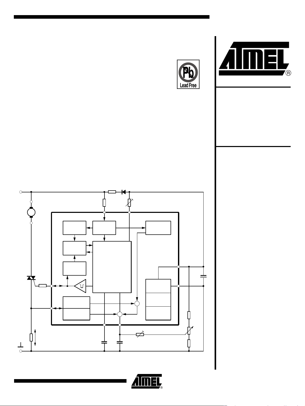
Figure 1-1. Block Diagram with Typical Circuit: Load Current Sensing
230 V ~
R
6
Load
TIC
226
R
3
8
180 Ω
1
^
V(R6) = ±250 mV
Limiting
detector
Automatic
retriggering
Current
detector
Full wave load
current
detector
Soft start
R
330 kΩ
C
22 kΩ/2 W
R
2
7
Voltage
detector
Phase
control unit
ϕ = f(V
23
3
100 nF3.3 nF
BYT51K
D
1
α
max
R
1
8
1 MΩ
6
Mains voltage
compensation
U2008B
-V
5
)
3
Supply
voltage
limiting
Reference
-
+
R
C
4
Load current
compensation
10
voltage
Voltage
monitoring
100 kΩ
4
Set point
GND
R
7
S
22 µF/
25 V
R
47 kΩ
P
C
1
14
1
Phase-control
IC with
Soft Start
U2008B
Rev. 4712B–AUTO–10/05
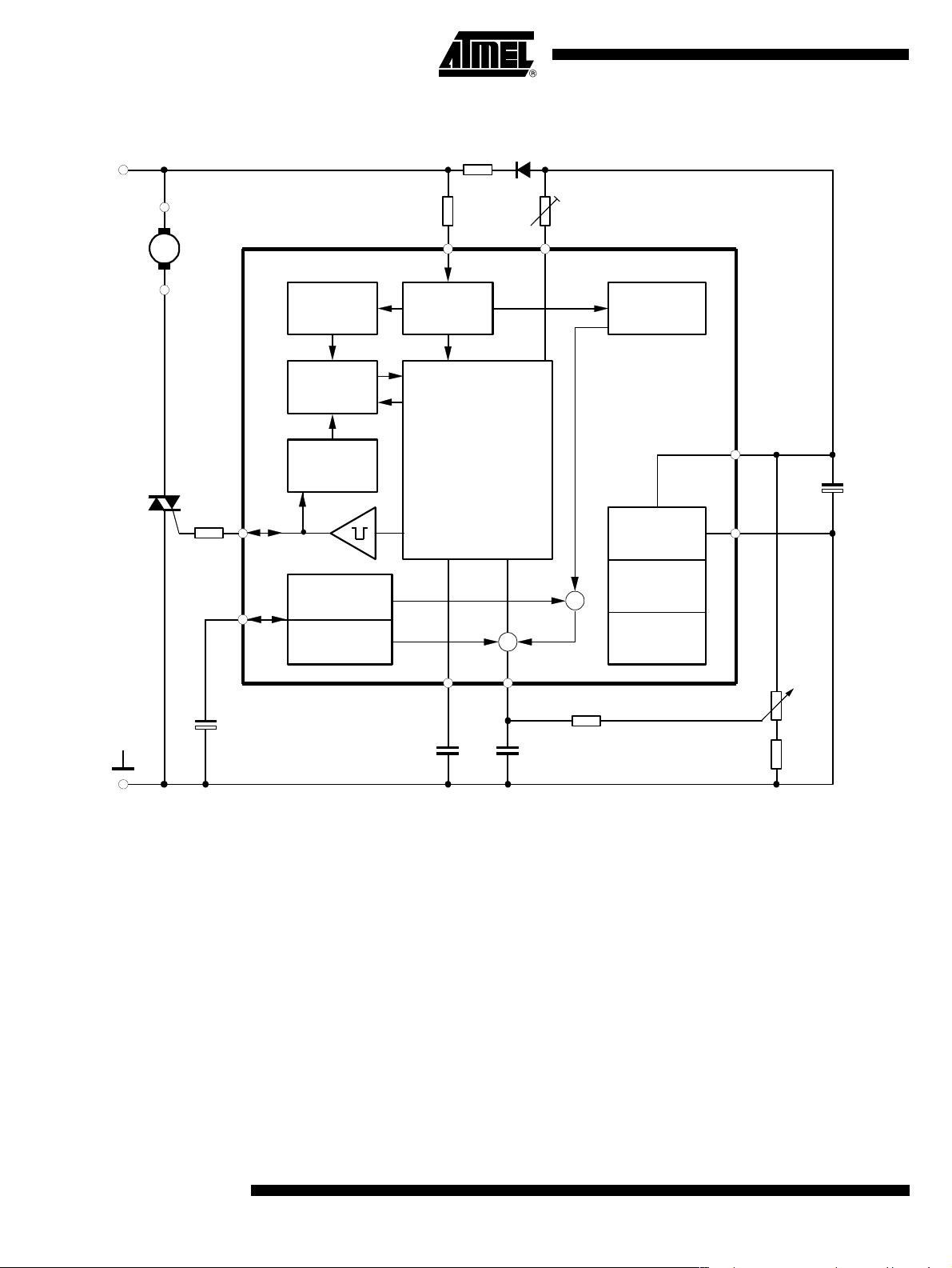
Figure 1-2. Block Diagram with Typical Circuit: Soft Start
230 V ~
L
TIC
226
Load
R
180 Ω
BYT51K
D
1
R
α
max
8
470 kΩ
6
Mains voltage
compensation
Limiting
detector
R
680 kΩ
22 kΩ/2W
2
Voltage
detector
R
1
7
Automatic
retriggering
Current
detector
Phase
control unit
ϕ = f(V
)
3
U2008B
-V
5
S
C
1
100 µF/
8
3
1
current detector
Full wave load
-
+
Soft start
Supply
voltage
limiting
Reference
voltage
Voltage
monitoring
25 V
GND
4
23
P
R
68 kΩ
C
5
Soft start
4.7 µF/25 V
C
3
C
4
10
100 nF10 nF
Set point
R
220 kΩ
7
1
50 kΩ
N
2
U2008B
4712B–AUTO–10/05
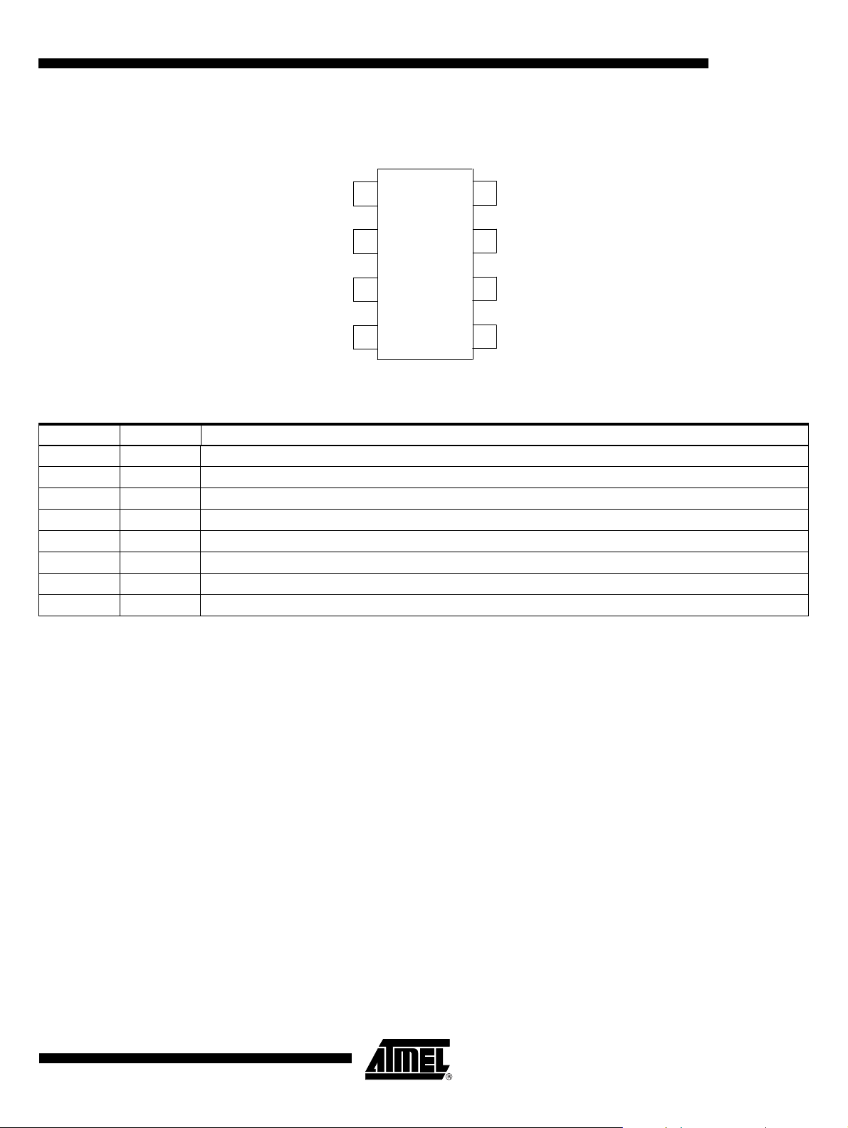
2. Pin Configuration
Figure 2-1. Pinning
U2008B
ISENSE
CONTROL
GND
Table 2-1. Pin Description
Pin Symbol Function
1 ISENSE Load current sensing
2Cϕ Ramp voltage
3 CONTROL Control input/compensation output
4 GND Ground
5 -VS Supply voltage
6Rϕ Ramp current adjustment
7 VSYNC Voltage synchronization
8 OUTPUT Trigger output
Cϕ
1
2
U2008B
3
4
8
7
6
5
OUTPUT
VSYNC
Rϕ
- VS
2.1 Mains Supply, Pin 5
The integrated circuit U2008B, which also contains voltage limiting, can be connected via D1 and
to the mains supply, see Figure 1-2 on page 2. Supply voltage, between Pin 4 (pos., ⊥) and
R
1
Pin 5, is smoothed by C
The series resistance R1 can be calculated as follows:
R
1max
where:
V
M
V
Smax
I
tot
I
Smax
I
x
Operation with externally stabilized DC voltage is not recommended.
.
1
–
V
MVSmax
------------------------------
0.85
×=
2I
×
tot
= Mains voltage
= Maximum supply voltage
= I
+ Ix = Total current compensation
Smax
= Maximum current consumption of the IC
= Current consumption of the external components
4712B–AUTO–10/05
3

2.2 Voltage Monitoring
When the voltage is built up, uncontrolled output pulses are avoided by internal voltage monitoring. Apart from that, all latches of the circuit (phase control, load limit regulation) are reset and
the soft start capacitor is short circuited. This guarantees a specified start-up behavior each time
the supply voltage is switched on or after short interruptions of the mains supply. Soft start is initiated after the supply voltage has been built up. This behavior guarantees a gentle start-up for
the motor and automatically ensures the optimum run-up time.
2.3 Phase Control, Pin 6
The function of the phase control is identical to that of the well-known IC U211B. The phase
angle of the trigger pulse is derived by comparing the ramp voltage V
on the control input, Pin 3. The slope of the ramp is determined by C
ϕ.
at Pin 2 with the set value
2
and its charging current I
3
The charging current can be regulated, changed or altered using R
The maximum phase angle, α
using R
(see Figure 5-1 on page 7).
8
When the potential on Pin 2 reaches the set point level of Pin 3, a trigger pulse is generated
whose pulse width, t
the same time, a latch is set with the output pulse, as long as the automatic retriggering has not
been activated, then no more pulses can be generated in that half cycle. Control input at Pin 3
(with respect to Pin 4) has an active range from -9 V to -2 V. When V
at its maximum amax, i.e., the current flow angle is minimum. The minimum phase angle amin is
set with V
≥ -1 V.
3
2.4 Automatic Retriggering
The current-detector circuit monitors the state of the triac after triggering by measuring the voltage drop at the triac gate. A current flow through the triac is recognized when the voltage drop
exceeds a threshold level of typically 40 mV.
If the triac is quenched within the relevant half wave after triggering (for example owing to low
load currents before or after the zero crossing of current wave, or for commutator motors, owing
to brush lifters), the automatic retriggering circuit ensures immediate retriggering, if necessary
with a high repetition rate, t
2.5 Current Synchronization, Pin 8
Current synchronization fulfils two functions:
at Pin 6.
8
, (minimum current flow angle ϕ
max
, is determined from the value of C3 (tp = 9 µs/nF, Figure 5-3 on page 8). At
p
, until the triac remains reliably triggered.
pp/tp
) can also be adjusted by
min
= -9 V the phase angle is
3
• Monitoring the current flow after triggering. In case the triac extinguishes again or it does not
switch on, automatic triggering is activated as long as triggering is successful.
• Avoiding triggering due to inductive load. In the case of inductive load operation, the current
synchronization ensures that in the new half wave no pulse is enabled as long as there is a
current available from the previous half wave, which flows from the opposite polarity to the
actual supply voltage.
A special feature of the IC is the realization of current synchronization. The device evaluates the
voltage at the pulse output between the gate and reference electrode of the triac. This results in
saving the separate current synchronization input with specified series resistance.
4
U2008B
4712B–AUTO–10/05

2.6 Voltage Synchronization with Mains Voltage Compensation, Pin 7
The voltage detector synchronizes the reference ramp with the mains supply voltage. At the
same time, the mains-dependent input current at Pin 7 is shaped and rectified internally. This
current activates automatic retriggering and at the same time is available at Pin 3 (Figure 5-5 on
page 9). By suitable dimensioning, it is possible to attain the specified compensation effect.
Automatic retriggering and mains voltage compensation are not activated until ⏐ V
increases to 8 V. The resistance R
synchronization current, and hence the mains supply voltage compensation current. If the mains
voltage compensation and the automatic retriggering are not required, both functions can be
suppressed by limiting ⏐ V
- V4⏐ ≤ 7 V (see Figure 2-2).
7
Figure 2-2. Suppression of Automatic Retriggering and Mains Voltage Compensation
defines the width of the zero voltage cross-over pulse,
sync.
Mains
R
2
7
U2008B
- V4⏐
7
A further feature of the IC is the selection between soft start and load-current compensation.
Soft start is possible by connecting a capacitor between Pin 1 and Pin 4 (Figure 5-4 on page 8).
In the case of load-current compensation, Pin 1 is directly connected with resistance R
used for sensing load current.
2.7 Load Current Detection, Pin 1
The circuit continuously measures the load current as a voltage drop at resistor R6. The evaluation and use of both half waves results in a quick reaction to load-current change. Due to voltage
at resistor R
internal current source, whose positive current values are available at Pin 3 (see Figure 5-7 on
page 9). The output current generated at Pin 3 contains the difference from the load-current
detection and the mains-voltage compensation (see Figure 5-5 on page 9).
The effective control voltage is the final current at Pin 3 together with the desired value network.
An increase of mains voltage causes an increase of the control angle α. An increase of load cur-
rent results in a decrease of the control angle. This avoids a decrease in revolution by increasing
the load as well as an increase of revolution by the increment of mains supply voltage.
, there is an increase of input current at Pin 1. This current increase controls the
6
2x
BZX55
C6V2
U2008B
4
, which is
6
4712B–AUTO–10/05
5

3. Absolute Maximum Ratings
VS = 14 V, reference point Pin 4, unless otherwise specified
Parameters Symbol Value Unit
30 mA
100 mA
5
20
VS to 0 V
500 mA
0.5 mA
1mA
-VS to +2 V
2
V
S
-40 to +125 °C
-10 to +125 °C
±I
±i
-I
-i
syncV
syncV
Current limitation Pin 5
t ≤ 10 µs
Synchronous currents Pin 7
t ≤ 10 µs
Phase Control Pin 3
Control voltage -V
Input current ±I
Charge current Pin 6 -I
ϕmax
Load Current Monitoring/Soft Start, Pin 1
Input current I
Input voltage V
Pulse output
Input voltage Pin 8
+V
-V
Storage temperature range T
Junction temperature range T
S
S
I
I
I
I
I
I
stg
j
mA
mA
V
V
4. Thermal Resistance
Parameters Symbol Value Unit
Junction ambient
DIP8 R
SO8 on p.c. R
So8 on ceramic R
thJA
thJA
thJA
110 K/W
220 K/W
140 K/W
5. Electrical Characteristics
Parameters Test Conditions Symbol Min. Typ. Max. Unit
Supply (Pin 5)
-I
= 3.5 mA
Supply-voltage limitation
S
= 30 mA
-I
S
Current requirement Pins 1, 4 and 7 open -I
Voltage Monitoring (Pin 5)
Turn-on threshold -V
Phase Control
Input current
Voltage limitation ±I
Voltage sync. Pin 7
Current sync. Pin 8
= 2 mA Pin 7 ±V
L
Reference Ramp (see Figure 5-1 on page 7)
Charge current Pin 7 I
Start voltage Pin 2 -V
±I
±I
-V
-V
TON
syncV
syncI
syncV
ϕ
max
S
S
S
14.5
14.6
16.5
16.8
3.0 mA
11.3 12.3 V
0.15 2
3
30
8.0 8.5 9.0 V
1 100 µA
1.85 1.95 2.05 V
V
V
mA
µA
6
U2008B
4712B–AUTO–10/05

U2008B
5. Electrical Characteristics (Continued)
Parameters Test Conditions Symbol Min. Typ. Max. Unit
Temperature coefficient of start
voltage
Pin 2 -TC
Rϕ - reference voltage Iϕ = 10 µA, Pins 6 to 5 V
Temperature coefficient
= 10 µA, Pin 6
I
ϕ
Iϕ = 1 µA
TC
TC
Pulse Output (see Figure 5-2 on page 8) (Pin 8)
Output-pulse current V
Output-pulse width C
= -1.2, RGT = 0 Ω I
8
= 3.3 nF, VS = V
3
limit
Automatic Retriggering (Pin 8)
Turn-on threshold voltage ±V
Repetition rate I
≥ 150 µA t
7
Soft Start (see Figure 5-4 on page 8) (Pin 1)
Starting current V
Final current V
= 8 V I
1–4
= -2 V I
1–4
Discharge current -I
Output current Pin 3 -I
Mains Voltage Compensation (see Figure 5-5 on page 9)
Current transfer gain I
7/I3
Reverse current V
Load-current Detection, V
= 0 (see Figure 5-7 on page 9)
7
Transfer gain I
Offset current V
Pins 7, Pin 3
Pins 1 and 2 open
= V3 = V7 = 0, Pin 3 ±I
(R6)
3/V1
= 0, V3 = -8 V, Pin 3 I
1
G
Input voltage Pin 1 -V
Input offset voltage Pin 1 ±V
R
0.96 1.02 1.10 V
100 125 150 mA
20 60 mV
357.5t
51015µA
15 25 40 µA
0.5 mA
0.2 2 mA
14 17 20
t
Rϕ
VRϕ
VRϕ
0
p
ION
pp
0
0
0
0
i
R
G 0.28 0.32 0.37 µA/mV
0
I
0
036µA
300 400 mV
-0.003 %/K
0.03
0.06
30 µs
2µA
6mV
%/K
%/K
p
4712B–AUTO–10/05
Figure 5-1. Ramp Control
250
200
33 nF 10 nF
150
100
Phase Angle α (°)
50
0
0 200 400 600 800 1000
6.8 nF 4.7 nF 3.3 nF
Rϕ(R8) (kΩ)
2.2 nF
Cϕ/t = 1.5 nF
7

Figure 5-2. Pulse Output
120
100
80
)
A
m
(
60
T
G
I
40
20
VGT = -1.2 V
0
0 200 400 600 800
Figure 5-3. Output Pulse Width
400
∆tp/∆Cϕ = 9 µs/nF
300
200
(µs)
p
t
100
0
0102030
Figure 5-4. Option Soft Start
1
1000
RGT (Ω)
Cϕ (nF)
0
-1
)
V
(
4
-
-2
1
V
-3
-4
-5
01 2 3 4
8
U2008B
C5 = 1 µF
4.7 µF
Supply
= 22 kΩ/2 W
R
1
= 100 µF/25 V
C
1
t ( s )
10 µF
5
4712B–AUTO–10/05

Figure 5-5. Mains Voltage Compensation
0
-40
-80
(µA)
3
I
-120
U2008B
-160
Pins 1
= -13 V
V
-200
S
-2 -1 0 1 2
Figure 5-6. Maximum Resistance of R
100
80
)
Ω
k
(
x
60
a
m
1
R
40
20
0
02 4 6 8
Figure 5-7. Load-current Detection
Reference Point
Pin 10
I7 (mA)
1
Max. Series Resistance
= 230 V
V
M
IS (mA)
1
0
4712B–AUTO–10/05
200
V6 = Ref = V
VS = -13 V
V
160
120
(µA)
5
I
80
40
0
-400 -200 0 200 400
= V10 = 0 V
15
8
V
(R6)
Reference Point
Pin 8
(mV)
9

Figure 5-8. Power Dissipation of R
10
Power Dissipation at Series Resistance R
8
)
6
W
(
V
P
4
2
1
1
0
010203040
R1 (kΩ)
50
Figure 5-9. Power Dissipation of R1 According to Current Consumption
10
Power Dissipation at Series Resistance
8
6
(W)
V
P
4
2
0
0 3 6 9 12 15
IS (mA)
10
U2008B
4712B–AUTO–10/05

6. Ordering Information
Extended Type Number Package Remarks
U2008B-xY DIP8 Tube, Pb-free
U2008B-xFPY SO8 Tube, Pb-free
U2008B-xFPG3Y SO8 Taped and reeled, Pb-free
7. Package Information
Package DIP8
Dimensions in mm
0.58
0.48
1.64
1.44
7.62
9.8
9.5
2.54
0.5 min
4.8 max
3.3
7.77
7.47
6.4 max
0.36 max
9.8
8.2
U2008B
Package SO8
Dimensions in mm
0.4
85
technical drawings
according to DIN
sp e c ific atio ns
14
5.00
4.85
1.4
0.25
1.27
3.81
85
0.10
5.2
4.8
3.7
0.2
3.8
6.15
5.85
4712B–AUTO–10/05
14
technical drawings
according to DIN
specifications
11

8. Revision History
Please note that the following page numbers referred to in this section refer to the specific revision
mentioned, not to this document.
Revision No. History
4712B-AUTO-08/05
• Put datasheet in a new template
• First page: Pb-free logo added
• Page 11: Ordering Information changed
12
U2008B
4712B–AUTO–10/05

Atmel Corporation Atmel Operations
2325 Orchard Parkway
San Jose, CA 95131, USA
Tel: 1(408) 441-0311
Fax: 1(408) 487-2600
Regional Headquarters
Europe
Atmel Sarl
Route des Arsenaux 41
Case Postale 80
CH-1705 Fribourg
Switzerland
Tel: (41) 26-426-5555
Fax: (41) 26-426-5500
Asia
Room 1219
Chinachem Golden Plaza
77 Mody Road Tsimshatsui
East Kowloon
Hong Kong
Tel: (852) 2721-9778
Fax: (852) 2722-1369
Japan
9F, Tonetsu Shinkawa Bldg.
1-24-8 Shinkawa
Chuo-ku, Tokyo 104-0033
Japan
Tel: (81) 3-3523-3551
Fax: (81) 3-3523-7581
Memory
2325 Orchard Parkway
San Jose, CA 95131, USA
Tel: 1(408) 441-0311
Fax: 1(408) 436-4314
Microcontrollers
2325 Orchard Parkway
San Jose, CA 95131, USA
Tel: 1(408) 441-0311
Fax: 1(408) 436-4314
La Chantrerie
BP 70602
44306 Nantes Cedex 3, France
Tel: (33) 2-40-18-18-18
Fax: (33) 2-40-18-19-60
ASIC/ASSP/Smart Cards
Zone Industrielle
13106 Rousset Cedex, France
Tel: (33) 4-42-53-60-00
Fax: (33) 4-42-53-60-01
1150 East Cheyenne Mtn. Blvd.
Colorado Springs, CO 80906, USA
Tel: 1(719) 576-3300
Fax: 1(719) 540-1759
Scottish Enterprise Technology Park
Maxwell Building
East Kilbride G75 0QR, Scotland
Tel: (44) 1355-803-000
Fax: (44) 1355-242-743
RF/Automotive
Theresienstrasse 2
Postfach 3535
74025 Heilbronn, Germany
Tel: (49) 71-31-67-0
Fax: (49) 71-31-67-2340
1150 East Cheyenne Mtn. Blvd.
Colorado Springs, CO 80906, USA
Tel: 1(719) 576-3300
Fax: 1(719) 540-1759
Biometrics/Imaging/Hi-Rel MPU/
High Speed Converters/RF Datacom
Avenue de Rochepleine
BP 123
38521 Saint-Egreve Cedex, France
Tel: (33) 4-76-58-30-00
Fax: (33) 4-76-58-34-80
Literature Requests
www.atmel.com/literature
Disclaimer: The information in this document is provided in connection with Atmel products. No license, express or implied, by estoppel or otherwise, to any
intellectual property right is granted by this document or in connection with the sale of Atmel products. EXCEPT AS SET FORTH IN ATMEL’S TERMS AND CONDI-
TIONS OF SALE LOCATED ON ATMEL’S WEB SITE, ATMEL ASSUMES NO LIABILITY WHATSOEVER AND DISCLAIMS ANY EXPRESS, IMPLIED OR STATUTORY
WARRANTY RELATING TO ITS PRODUCTS INCLUDING, BUT NOT LIMITED TO, THE IMPLIED WARRANTY OF MERCHANTABILITY, FITNESS FOR A PARTICULAR
PURPOSE, OR NON-INFRINGEMENT. IN NO EVENT SHALL ATMEL BE LIABLE FOR ANY DIRECT, INDIRECT, CONSEQUENTIAL, PUNITIVE, SPECIAL OR INCIDENTAL DAMAGES (INCLUDING, WITHOUT LIMITATION, DAMAGES FOR LOSS OF PROFITS, BUSINESS INTERRUPTION, OR LOSS OF INFORMATION) ARISING OUT
OF THE USE OR INABILITY TO USE THIS DOCUMENT, EVEN IF ATMEL HAS BEEN ADVISED OF THE POSSIBILITY OF SUCH DAMAGES. Atmel makes no
representations or warranties with respect to the accuracy or completeness of the contents of this document and reserves the right to make changes to specifications
and product descriptions at any time without notice. Atmel does not make any commitment to update the information contained herein. Unless specifically provided
otherwise, Atmel products are not suitable for, and shall not be used in, automotive applications. Atmel’s products are not intended, authorized, or warranted for use
as components in applications intended to support or sustain life.
© Atmel Corporation 2005. All rights reserved. Atmel®, logo and combinations thereof, Everywhere You Are® and others, are registered trade-
marks or trademarks of Atmel Corporation or its subsidiaries. Other terms and product names may be trademarks of others.
Printed on recycled paper.
4712B–AUTO–10/05
 Loading...