


ADC 10-bit 2 Gsps Evaluation
Board - TSEV83102G0B
..............................................................................................
User Guide

Table of Contents
Section 1
Overview...............................................................................................1-1
1.1 Description................................................................................................1-1
1.2 TSEV83102G0B Evaluation Board...........................................................1-2
1.3 Board Mechanical Characteristics.............................................................1-3
1.4 Analog Input, Clock Input and De-embedding Fixture Accesses..............1-4
1.5 Digital Outputs Accesses ..........................................................................1-4
1.6 Power Supplies and Ground Access es.................. ...... ....... ...... ................1-4
1.7 ADC Function Setting Accesses...............................................................1-4
Section 2
Layout Information................................................................................2-1
2.1 Board ........................................................................................................2-1
2.2 AC Inputs/Digital Outputs................................ ....... ...... ....... ...... ....... ...... ...2-1
2.3 DC Function Settings ................................................................................2-1
2.4 Power Supplies.........................................................................................2-2
Section 3
Operating Procedur es and
Characteristics......................................................................................3-1
3.1 Introduction ...............................................................................................3-1
3.2 Operating Procedure (ECL Mode) ............................................................3-1
3.3 Use with DMUX Evaluation Board ............................................................3-2
3.4 Electrical Characteristics...........................................................................3-3
3.5 Operating Charcteristics............................................................................3-4
Section 4
Application Information.................................. .... ...................................4-1
4.1 Introduction ...............................................................................................4-1
4.2 Analog Inputs............................................................................................4-1
4.3 Clock Inputs ..............................................................................................4-1
4.4 Setting the Digital Output Data Format.....................................................4-1
4.5 ADC Gain Adjust.......................................................................................4-2
4.6 SMA Connectors and Microstrip Lines De-embedding Fixture .................4-2
4.7 Die Junction Temperature Monitoring.......................................................4-3
4.8 Decimation Function .................................................................................4-5
4.9 Pattern Generator Enable .........................................................................4-5
4.10 Data Ready Output Signal Reset..............................................................4-6
4.11 Sampling Delay Adjusting .........................................................................4-6
4.12 Test Bench Description.............................................................................4-7
TSEV83102G0B - Evaluation Board User Guide i
2166B–BDC–04/03

Table of Contents
Section 5
Package Description.............................................................................5-1
5.1 TS83102G0B Pinout.................... ...... ....... ...... ....... ...... ....... ...... ....... .........5-1
5.2 Thermal Characteristics............................................................................5-3
5.2.1 Thermal Resistance from Junction to Ambient: Rthja ........................5-3
5.2.2 Thermal Resistance from Junction to Case: Rthjc .............................5-4
5.2.3 Heatsink..............................................................................................5-4
5.3 Ordering Information.................................................................................5-5
Section 6
Schematics...........................................................................................6-1
6.1 TSEV83102G0B Electrical Schematic......................................................6-1
ii TSEV83102G0B - Evaluation Board User Guide
2166B–BDC–04/03

Section 1
Overview
1.1 Description
The TSEV83102G0B Evaluati on Board (EB) is a p rototype board which has been
designed in order to facilitate the evaluation and the characterization of the
TS83102G0B device (in CBGA152) up to its 3 GHz full power bandwidth at up to 2 Gsps
in the extended temperature range.
The high speed of th e TS831 02G0 B requi res careful atten tion t o ci rcuit d esig n and layout to achieve optimal per formanc e. This four met al layer board w ith an inter nal groun d
plane has the function s that allow a quic k and simple ev aluation of the TS83102G0B
ADC performances over the temperature range.
The TS83102G0B Evaluation Board (EB) is very straightforward as it only implements
the TS83102G0B ADC device, SMA connectors for input/output accesses and a
2.54 mm pitch connec tor com patible with high speed ac qui siti on s y ste m hig h freq uen cy
probes.
The board has been desi gned to be fully co mpatible with Atme l’s DMUX evaluatio n
board (TSEV81102G0).
The board also implements a de-embedding fixture in order to facilitate the evaluation of
the high frequency insertion loss of the input microstrip lines.
The board is constructed l ike a sand wich of two dielec tric layers , featuring low inser tion
loss and enhanced thermal characteristics for operation in the high frequency domain
and extended temperature range.
The board dimensions are 120 mm x 150 mm.
The board set comes fully assembled and tested, with the TS83102G0B installed and
with a heatsink.
TSEV83102G0B - Evaluation Board User Guide 1-1
Rev. 2166B–BDC–04/03

Overview
1.2 TSEV83102G0B
Evaluation Board
Figure 1-1. TSEV83102G0B Block Diagram
CLK
Differential
Clock inputs
CLKB
VIN
Differential
analog inputs
VINB
TEST
GAIN
Z0 = 50Ω
Z0 = 50Ω
Z0 = 50Ω
Z0 = 50Ω
VEE
CLK
CLKB
TS83102G0B
VIN
VINB
GA
PGEB
DRRB
VCC
GND
VPLUSD
VEE
DR/DRB
D0/D0B
D7/D7B
PC/PCB
VCC = +5V
GND = 0V
VPLUSD = -0.8V (ECL)
VPLUSD = 1.6V (LVDS)
VEE = -5V
Z0 = 50Ω
Z0 = 50Ω
Z0 = 50Ω
Z0 = 50Ω
DRRB
CAL1
CAL2
VCC
VEE
GND
DVEE
SDA
OA
+5V
+5V
+5V
DVEE
SDA
SDAEN
L = 50 mm typ
LVIN/VINb = LCLK/CLKb = 43 mm typ
Loutputs = 58 mm typ
Short-circuit
possibility
here
DIODE
DVEE = -5V
J - diode
V - diode
VEE
B/BG
V-GND
I-GND
1-2 TSEV83102G0B - Evaluation Board User Guide
2166B–BDC–04/03
Overview
1.3 Board
Mechanical
Characteristics
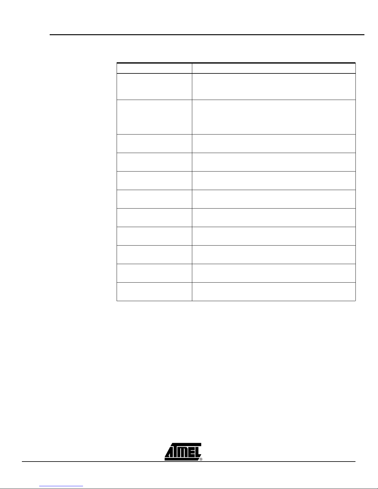
The board’s layer number, thickness, and functions are given below, from top to bottom.
Table 1-1. Board’s Layer Thickness Profile
Layer Characteristics
Layer 1
Copper layer
Layer 2
RO4003 dielectric layer
(Hydrocarbon/Wovenglass)
Layer 3
Copper layer
Layer 4
BT/Epoxy dielectric layer
Layer 5
Copper layer
Layer 6
BT/Epoxy dielectric layer
Layer 7
Copper layer
Copper thickness = 40 µm
AC signal traces = 50Ω microstrip lines
DC signal traces (B/GB, GAIN, DIODE, OA, TEST, SDA)
Layer thickness = 200 µm
Dielectric constant = 3.4 at 10 GHz
-0.044 dB/inch insertio n loss at 2.5 GHz
-0.318 dB/inch insertion loss at 18 GHz
Copper thickness = 39 µm
Ground plane = reference plane 50Ω microstrip return
Layer thickness = 330 µm
Copper thickness = 35 µm
Power and ground planes
Layer thickness = 330 µm
Copper thickness = 35 µm
Power and ground planes (identical to layer 5)
Layer 8
BT/Epoxy dielectric layer
Layer 9
Copper layer
Layer 10
BT/Epoxy dielectric layer
Layer 11
Copper layer
Layer thickness = 330 µm
Copper thickness = 35 µm
Ground planes (identical to layer 3)
Layer thickness = 200 µm
Copper thickness = 35 µm
Power and ground planes
The TSEV83102G0B is an ele ven la yer PC B made of s ix copper laye rs and five die lectric layers. The si x metal la yers corres pond respec tively from top to bottom to the A C
and DC signals layer (layer 1), two ground layers (layers 3 and 5), and one supply layer
(layer 7).
Considering the s evere mec hanica l constr aints due to the wide temperat ure rang e and
the high frequency domain in which the board is to operate, it is necessary to use a
sandwich of two different dielectric materials, with specific characteristics:
A low insertion loss RO4003 Hydrocarbon/Wovenglass dielectric layer of 200 µm
thickness, chosen for its low loss (-0.318 dB/inch) and enhanced dielectric
consistency in the high frequency domain. The RO4003 dielectric layer is dedicated
to the routing of the 50Ω impedance signal traces (the RO4003 typical dielectric
constant is 3.4 at 10 GHz). The RO4003 dielectric layer characteristics are very close
to PTFE in terms of insertion loss characteristics.
A BT/Epoxy dielectric layer of 0.9 mm total thickness which is sandwiched between
the upper ground plane and the back-side supply layer.
TSEV83102G0B - Evaluation Board User Guide 1-3
2166B–BDC–04/03

Overview
The BT/Epoxy layer has been ch os en be ca us e of i ts e nhanced mechanical charac teri stics for elevated temperature operation. The typical dielectric constant is 4.5 at 1 MHz.
More precisely, the BT/E poxy diel ectric layer offe rs enha nced ch aracteris tics co mpare d
to FR4 Epoxy, namely:
Higher operating temperature values: 170°C (125°C for FR4).
Better withstanding of thermal shocks (-65°C up to 170°C).
The total board thi ckness is 1.6 mm. The prev iously desc ribed mechani cal and frequency characteristics makes the board particularly suitable for device evaluation and
characterization in the high frequency domain and in military temperature ranges.
1.4 Analog Input,
Clock Input and
De-embedding
Fixture Access es
1.5 Digital Outputs
Accesses
1.6 Power Supplies
and Ground
Accesses
1.7 ADC Function
Setting Accesse s
The differential active inputs (Analog, Clock, De-embedding fixture) are provided by
SMA connectors.
Reference: VITELEC 142-0701-851.
Connector mounting plates have been used for fastening the SMA connectors.
Access to the differential output data port is provided by a 2.54 mm pitch connector,
compatible with the high spee d digital acqui sition syst em. It enables acc ess to the converter output data, as well as proper 50Ω differential termination.
The power supply accesses are provided by five 2 mm section banana jacks respectively for DV
The power supply access is provided by one 4 mm section banana jack for V
The Ground accesses are provided by four 2 mm and one 4 mm banana jacks.
For ADC function setting accesses (B/GB, Die junction temp., Test), 2 mm section
banana jacks are provided.
Three potentiometers a re provided for ADC gain adj us t, S am pli ng de la y adj ust and O ffset adjust.
EE
, V
EET
, VDD, V
PLUSD
and VCC.
EE
.
One sub-screw is provided for Asynchronous data ready reset.
1-4 TSEV83102G0B - Evaluation Board User Guide
2166B–BDC–04/03

Section 2
Layout Information
2.1 Board
2.2 AC Inputs/Digital
Outputs
The TS83102G0B requires proper board layout for optimum full speed operation.
The following explains th e board l ayout recomm endations a nd demonstrates how the
Evaluation Board fulfills these implementation constraints.
A single low impedance ground plane is rec ommended, since it allows the user to lay
out signal traces and power planes without interrupting the ground plane.
Therefore a multi-layer board structure has been retained for the TSEV83102G0B.
Six copper metal layers are used, dedicated respectively (from top to bottom) to the sig-
nal traces, ground planes and power supplies.
The board uses 50Ω impedance micros trip line s for the diffe rentia l analog i nputs, cloc k
inputs, and differential digital outputs.
The input signals an d c lock si gna ls mus t b e r oute d on one l ay er on ly, without using any
through-hole vias. The line lengths are matched to within 2 mm.
The digital output lines are 50Ω differentially terminated.
The output data trace lengths are matched to within 0.25 inch (6 mm) to min imize the
data output delay skew.
For the TSEV83102G0B the propagation delay is approximately 6.1 ps/mm
(155 ps/inch). The RO4003 typical dielectric constant is 3.4 at 10 GHz.
For more informations about different output termination options refer to the specifica-
tion application notes.
2.3 DC Function
Settings
TSEV83102G0B - Evaluation Board User Guide 2-1
The DC signal traces are low impedance.
They have been routed with a 50Ω impeda nce near the devic e because of spac e
restriction.
Rev. 2166B–BDC–04/03

Layout Information
2.4 Power Supplies
The bottom metal layers 5 and 7 and 11 are dedicated to power supply traces (VEE,
DV
, V
EE
, VDD, V
EET
PLUSD
and VCC).
The supply traces are approximately 6 mm wide in order to present low impedance, and
are surrounded by a ground plane connected to the two inner ground planes.
The analog and digital negative power supply traces are independent, but the possibility
exists to short-circuit both supplies on the top metal layer).
No difference in ADC high speed performance is observed when connecting both negative supply planes together. Obviously one single negative supply plane could be used
for the circuit.
Each power supply incoming is bypassed by a 1 µF Tantalum capacitor in parallel with
1 nF chip capacitor.
Each power supply access is decoupled very close to the device by 10 nF and 100 pF
surface mount chip capacitors in parallel.
Note: The decoupling capacitors are superposed. In this configuration, the 100 pF capacitors
must be mounted first.
2-2 TSEV83102G0B - Evaluation Board User Guide
2166B–BDC–04/03

Section 3
Operating Procedures and
Characteristics
3.1 Introduction
3.2 Operating
Procedure (ECL
Mode)
This section describes a typical single-ended configuration for analog inputs and clock
inputs.
The single-ended configuration is preferable, as it corresponds to the most straightforward and quickest TSEV83102G0B board setting for evaluating the TS83102G0B at full
speed in its temperature range.
The inverted analog input V
(on-chip 50Ω terminated). In this configuration, no balun transformer is needed to convert properly the single-ended mixer output to balanced differential signals for the
analog inputs.
In the same way, no balun is neces sary to feed the TS 83102 G0B c lock i nputs with ba lanced signals.
Directly connect the RF sources to the in-pha se analog and clock inp uts of the
converter.
However, dynamic per formanc es ca n b e so mewhat impr oved by en terin g ei ther ana log
or clock inputs in differential mode.
1. Connect the power supplies and Ground accesses
(V
= +5V, GND = 0V, V
CC
banana jacks.
The -5V power supplies should be turned on first.
and clock input CLKB common mode level is Ground
INB
= 0V, VEE = DVEE = -5V) through the dedicated
PLUSD
2. The board is set by default for digital outputs in binary format.
3. Connect the CLK clock signal.
TSEV83102G0B - Evaluation Board User Guide 3-1
Note: one single -5V power supply can be used for supplying the digital DV
analog V
The inverted phase clock input CLKB may be left open (as on-chip 50Ω terminated). Use a low phase noise RF source. The clock input level is typically
4 dBm and should not exceed +10 dBm into the 50Ω termination resistor (maximum ratings for the clock input power level is 15 dBm).
power planes.
EE
Rev. 2166B–BDC–04/03
EE
and

Operating Procedures and Ch aracteristics
3.3 Use with DMUX
Evaluation Board
4. Connect the analog signal VIN. The inverted phase clock input V
may be left
INB
open (as on cavity 50Ω terminated). Use a low phase noise RF source. Full
scale range is 0.5V peak to peak around 0V, (±250 mV), or -2 dBm into 50Ω.
Input frequency can range from DC up to 1.8 GHz. At 3.0 GHz, the ADC attenuates the input signal by -3 dB. The board insertion loss (S21) will be furnished in
the definitive document release.
5. Connect the high speed data acquisition system probes to the output connector.
The connector pitch (2.54 mm) is compatible with high speed digital acquisition
system probes. The digital data are on-board differentially terminated. However,
the output data can be picked up either in single-ended or differential mode.
The TSEV81102G0 DMUX evaluation board has been designed to be fully compatible
with the TSEV83102G0B ADC evaluation board.
The DEMUX input configuration has been optimized to be connected to the
TS83102G0B ADC (CBGA152 pac ka ge).
When using the DEMUX boa rd with the A DC bo ar d, do not fo rget to se t, for prop er use ,
CLKINTYPE in mode DR/2 (jumper on-board).
The power-up sequence should be:
1. Supply the ADC first
2. Supply the DMUX
3. Perform an asynchronous reset on the DMUX board
When this power up sequence ha s been completed, th e synchroniza tion between th e
DEMUX and ADC boar ds can be ac hieved via the DEMU XDelA DjCtrl p otenti ometer o n
the DEMUX evaluation board. To achieve a good synchronization between the two
boards, it is recommended to run the ADC at its full speed (max sampling rate) and tune
the DEMUX Delay Adjust Control potentiometer to the left and take down the settings for
which the boards are de-synchronized and similarly to the right to see the loss of synchronization at the other extremity. The right setting of the potentiometer is in the middle
of these two settings and should be right for all sampling rates of the ADC.
Please refer to the "ADCs and Demux Application Notes" document for more
information.
3-2 TSEV83102G0B - Evaluation Board User Guide
2166B–BDC–04/03

Operating Procedures and Characteristics
3.4 Electrical
Characteristics
Table 3-1. Absolute Maximum Ratings
Parameter Symbol Comments Value Unit
Positive supply voltage V
Digital negative supply voltage DV
Digital positive supply voltage V
Negative supply voltage V
Maximum difference between negative supply voltages DV
Analog input voltages V
Maximum difference between VIN and V
INB
Clock input voltage V
Maximum difference between V
CLK
and V
CLKB
Static input voltage V
Digital input voltage V
Digital output voltage V
Maximum junction temperature T
Storage temperature T
Lead temperature (soldering 10s) T
IN
VIN - V
CLK
V
CLK
PLUSD
to V
EE
or V
or V
- V
leads
CC
EE
stg
D
D
O
EE
EE
INB
INB
CLKB
CLKB
GA/SDA -5 to +0.8 V
SDAEN, DRRB,
B/GB, PGEB
j
Note: Absolute maximum ratings are limiting values (referenced to GND = 0V), to be applied individually, while other parameters are
within specified operating conditions. Long exposure to maximum rating may affect device reliability. The use of a thermal heat
sink is mandatory.
GND to 5.5 V
GND to -5.5 V
GND -1.1 to 2.0 V
GND to -5.5 V
0.3 V
-1.5 to +1.5 V
-1.5 to +1.5 V
-1 to +1 V
-1 to +1 V
-5 to +0.8 V
V
PLUSD
-2.2 to V
PLUSD
+0.3 V
+125 °C
-65 to +150 °C
+300 °C
TSEV83102G0B - Evaluation Board User Guide 3-3
2166B–BDC–04/03

Operating Procedures and Ch aracteristics
3.5 Operating
Characteristics
The power supplies denoted by VCC, VEE, DVEE and V
TS83102G0B ADC.
The power supplies denoted V
, VDD are dedicated to the op tio nal MC100EL16 asyn-
EET
are dedicated to the
PLUSD
chronous differential rec eiv ers .
Table 3-2. Electrical Operating Characteristics
Value
Parameter Symbol
V
CC
Positive supply voltage
V
PLUSD
(dedicated to TS83102G0B ADC only)
V
EEA
V
EED
I
CC
Positive supply current
(dedicated to TS83102G0B ADC only)
Positive supply voltage not used by default – installed
(dedicated to MC100EL16 differential receivers)
Positive supply current not used by default – installed
(dedicated to MC100EL16 differential receivers)
I
PLUSD
I
EEA
I
EED
V
EET
V
I
EET
I
DD
DD
Nominal power dissipation (without receivers) PD – 4.6
Analog input impedance Z
IN
Full power analog input bandwidth (-3 dB) – – 3.0 – GHz
4.75 5 5.25 V
–
ECL: -0.8
LVDS: 1.6
–
-5.25 -5 -4.75 V
-5.25 -5 -4.75 V
– 144 205 mA
–164–mA
– 514 630 mA
– 170 180 mA
-5.25 -5 -4.75 V
-2.15 -2 -185 V
–180–mA
–480–mA
5.1
(T
= 125°C)
J
–50–Ω
UnitMin Typ Max
V
V
W
Analog input voltage range (differential mode) V
IN
-125 – 125 mV
Clock input impedance – – 50 – Ω
Clock input voltage compatibility (single-ended or
differential) (See Application Notes)
– ECL levels or 4 dBm (typ) into 50Ω –
Clock input power level into 50Ω termination resistor – -2 2 4 dBm
3-4 TSEV83102G0B - Evaluation Board User Guide
2166B–BDC–04/03

Section 4
Application Information
4.1 Introduction
4.2 Analog Inputs
4.3 Clock Inputs
For this section, also refer to the product "Main features" (TS83102G0B Datasheet).
More particularly, refer to sections related to single-ended and differential input
configurations.
The analog inpu ts can be e nte red in diff erent ial or si ngle-en ded m ode wit hout a ny hig h
speed performance degradation.
The board digi tizes singl e-e nded signal s b y choo sing eit her inpu t and lea ving th e oth er
input open, as the latter is on-board 50Ω terminated. The nominal in-phase inputs are
V
(See Section 3).
IN
The clock inputs can be en tered i n dif fer ent ial or si ngl e-end ed mo de wi thou t any perfor mance degradation for a clock frequency up to 500 MHz. At higher rates, it is
recommended to drive the clock inputs differentially. Moreover , the typical in phase
clock input amplitude is 1V peak to peak, centered on 0V (Ground), or -1.3V (ECL) on
common mode.
As for the analog input, either clock input can be chosen (if the single-ended output
mode is used), leaving the other input open, as both clock inputs are on-chip 50Ω terminated. The nominal in-phase clock input is CLK (Section 3).
4.4 Setting the
Digital Output
Data Format
TSEV83102G0B - Evaluation Board User Guide 4-1
For this section, refer to the Evaluation B oard Electrical s chematic and to the components placement docume nt (resp ectivel y Figur e 6-1 on pag e -2 and Fi gure 6-6 o n page
-3).
Refer also to the TS83102G0B specification about digital output coding.
The TS83102G0B delivers data in natural binary code or in Gray code. If the B/GB input
is left floating or tied to GND the data format selected will be natural binary, if this input
is tied to V
Use the jumper denoted B/GB to select the output data port format:
If B/GB is left floating or tied to GND, the data output format is true binary.
If B/GB is tied to V
format.
the data will follow the Gray code.
EE
or driven with ECL low level, the data outputs are in the Gray
EE
Rev. 2166B–BDC–04/03

Application Information
4.5 ADC Gain Adjust
The V
level from -1.05V (V
positive supply voltage allows the adjustment of the output common mode
PLUSD
= -0.8V for ECL output compatibility) to +1.35V (V
PLUSD
PLUSD
= 1.6V
for LVDS output compatibility).
Each output voltage v aries between -0.9V and -1.2V (res pectively +1 .2V and +1.5V),
leading to ±0.3V = 660 mV in differential for V
= -0.8V (respectively 1.6V).
PLUSD
The ADC gain is adjus table by the means of pin R9 ( pad input impedance is 1 MΩ in
parallel with 2 pF). A j umper den oted GAIN has been fo reseen in order to ha ve a ccess
to the ADC gain adjust pin.
The GAIN potentiometer is dedicated to adjusting the ADC gain from approximately
0.85 up to 1.15.
The gain adjust transfer function is given below.
Figure 4-1. ADC Gain Adjust
1.20
1.15
1.10
1.05
1.00
ADC Gain
0.95
4.6 SMA Connectors
and Microstrip
Lines Deembedding
Fixture
0.90
0.85
0.80
-600 -400 -200 0 200 400 600
Vgain (command voltage) (mV)
Attenuation in microstrip lines can be found by taking the differ ence in the log magnitudes of the S21 scattering parameters measured on two different lengths of
meandering transmission lines.
Such a measurem ent also removes co mmon los ses such as those due to transitio ns
and connectors.
The S21 scatter ing par ameter c orres ponds to the a mount of powe r tr ansmitte d thr ough
a two-port network.
The characteristic impedance of the microstrip meander lines must be close to 50Ω to
minimize impedance mismatch with the 50Ω network analyzer test ports.
Impedance mismatch will cause ripples in the S21 parameter as a function of both the
degree of mismatch and the length of the line.
4-2 TSEV83102G0B - Evaluation Board User Guide
2166B–BDC–04/03

Application Information
4.7 Die Junction
Temperature
Monitoring
Figure 4-2 and Figure 4-3 illustrate the recommanded implementation of the die junction
temperature monitoring function for the Revision B of the 10-bit 2 Gsps ADC.
The user has the choice between two possible configurations:
1. The ADC decimation test mode is NOT ALLOWED.
Because of the use of 1 internal diode-mounted transistors, the user has to implement
2 x 2 head-to-tail protection diodes to avoid potential reverse current flows to damage
the diode pin.
Note that Atmel usually reco mmends the use of 2 x 3 head-to-t ail protection di odes but
in this particular case, it is necessary to have exactly 2 diodes in the A10 to gr ound
direction of conduction.
Figure 4-2. Recommend ed Die J unctio n Tempe rature Monito ring Fun ction Im pleme ntation, Test Mode Not Allowed
IGND
ADC Pin
A10
GND
Idiode
Vdiode
VGND
1 mA
V
2. The ADC test mode can be allowed
In case the user wants to still be able to switch from the normal mode to the test mode or
to the die junct ion t empera ture m onito ring, the prot ectio n diod e conf igura tion is slig htly
different and takes into account the fact that the test mo de can be activated by applying
V
= -5V to the diode pin.
EE
This explains why 7 pro tec tio n di ode s a re nee ded in t he o t her di r ection, as described in
Figure 4-3.
Figure 4-3. Recommended Diode Pin Implementation Allowin g for Both Die Junction
Temperature Monitoring Function and Test Mode
IGND
ADC Pin
A10
Idiode
Vdiode
1 mA
V
TSEV83102G0B - Evaluation Board User Guide 4-3
GND
VGND
2166B–BDC–04/03

Application Information
For Revision B, the V
characteristic corresponds to a single diod e characteri stic
DIODE
over temperature, thus starting at 0.9V, as illustrated in Figure 4-4, which is only an
interpolated V
characteristic (to be confirmed by future measurements).
DIODE
This modification in Revis io n B de vi ce s i mpl ie s the mod ifi ca tio n of the pr oce ss i ng of th e
V
characteristic if any but above all, it allows the user to implement a digital temper-
DIODE
ature sensor to be interfaced with the ASIC (DSP, FPGA, etc...) loading the ADC.
Figure 4-4. Diode Pin Implementation in Test Mode
ADC Pin
A10
GND
VEE = -5V
A typical configuration with a standard digital temperature sensor is depicted in
Figure 4-5.
Figure 4-5. Typical Configuration with a Digital Temperature Sensor
A10
GND
DXT
Temperature
Sensor
DXN
4-4 TSEV83102G0B - Evaluation Board User Guide
2166B–BDC–04/03

Application Information
The expected diode mounted transistors V
tance) versus junction temperature is given in Figure 4-6 (I
value (including chip parasitic resis-
DIODE
DIODE
= 1 mA).
Figure 4-6. Junction Temperature Versus Diode Voltage for I = 1 mA
940
930
920
910
900
890
880
870
860
850
840
Diode Voltage (mV)
830
820
810
800
790
Note: The operating die junction temperature must be kept below 125°C; therefore, an ade-
quate cooling system has to be set up.
0-10 2010 4030 6050 8070 10090 110
Junction Temperature (°C)
4.8 Decimation
Function
4.9 Pattern
Generator
Enable
The decimation function can be used for debug of the ADC at initial stages. This function
indeed allows to reduce the ADC output rate by 32, thus allowing for a quick debug
phase of the ADC at maximum speed rate.
When active, this fuction makes the ADC output only 1 out of 32 data, thus resulting in a
data rate which is 32 times slower than the clock rate.
The TS83102G0B is able to generate by itself (without any analog input signal) a serie
of patterns. If the TEST input is left floating or ti ed to GND the TS831 02G0B wil l digiti z e
the analog input signal ac cording to B/G B. If this inp ut is driven with ECL lo w level or
tied to V
, TS83102G0B will generate Checker Board patterns.
EE
Use the jumper denoted TEST for enabling the pattern generator.
TSEV83102G0B - Evaluation Board User Guide 4-5
2166B–BDC–04/03

Application Information
4.10 Data Ready
Output Signal
Reset
4.11 Sampling Delay
Adjusting
A sub-screw connector is provided for the DRRB command.
The Data Ready signal is reset on the falling edge of the DRRB input command, on ECL
logical low level (-1.8V). DRRB may also be tied to V
nal master reset. As l ong as DRR B r em ai ns at a l ogi cal low level, (or tied to V
= -5V for Data Ready output sig-
EE
= -5V),
EE
the Data Ready output remains at logical zero and is independent of the external free
running encoding clock.
The Data Ready output signal (DR, DRB) is reset to logical zero after TRDR = 720 ps
typically.
TRDR is measured between th e -1.3V point of the falling edge o f the DRRB input c ommand and the zero crossing point of the differential Data Ready output signal (DR,
DRB).
The Data Ready Reset command may be a pulse of 1 ns minimum time width.
The Data Ready output signal restarts on th e DRRB comma nd rising edge, E CL logical
high levels (-0.8V).
DRRB may also be grounded, or is allowed to float, for normal free runn ing of the Data
Ready output signal.
One delay adjust, controlled by SDA potentiometer, is available in order to add a delay
to the input clock of the ADC. This allows the user to tune the instant of the internal sampling. To enable this delay adjustment there is an SDAEN pin on the chip. In the current
revision, the SDAEN function corresponds to the OA labels (OA jumper and OA
potentiometer).
Figure 4-7. Sampling Delay Adjust
: (cross(clip((VT("delop") - VT("delon")) 4e-10 2e-09) 0 2 "rising") - cross(clip((VT("delip") - VT("delin")) 2.5e-10 2e-09) 0 2 "rising")) (60°C)
400p
300p
Delay
200p
100p
-500m -400m -300m -200m -100m 100m
The OA potentiometer has been removed and short-circuited to V
EE
.
Use the jumper denoted OA to enable the sampling delay adjustment:
If OA is left floating or tied to GND, the SDA is disabled
If OA is tied to V
, the SDA is enabled
EE
The SDA input varies from -0.5 to 0.5V, according to the SDA potentiometer position.
The variation of the delay around its nominal value as a function of the SDA voltage is
more or less linear, as shown in Figure 4-7 (simulation results).
Delay in the variable delay cell at 60°C
200m 300m 400m 500m0m
SDAVAL
Note: The variation of the delay as a function of temperature is insignificant.
4-6 TSEV83102G0B - Evaluation Board User Guide
2166B–BDC–04/03

Application Information
4.12 Test Bench
Description
Figure 4-8. Differential Analog and Clock Input Configuration
RF Generator
-121 dBc/Hz at 1 KHz
offset from fc
Synchro 10 MHz
-117 dBc/Hz at 20 KHz
offset from fc
GPIB
RF Generator
Data Acquisition
System
PC
BPF
0 − 180°
Hybrid
10 Data
DR
Tunable delay line
CLKB CLK
TS83102G0B
ADC
0 − 180°
Hybrid
VINB
VIN
Figure 4-9. Single-ended Analog and Clock Input Configuration
RF Generator
BPF
Synchro 10 MHz
RF Generator
Data Acquisition
System
GPIB
PC
(50Ω) CLKB CLK
10 Data
DR
Tunable delay line
TS83102G0B
ADC
VINB (50Ω)
VIN
TSEV83102G0B - Evaluation Board User Guide 4-7
2166B–BDC–04/03

Section 5
Package Description
5.1 TS83102G0B
Pinout
Figure 5-1. TS83102G0B Pinout of CBGA152 Package
ABCDEFGHJKLMNPQR
16
15
14
13
12
11
10
D0
NC
GND
DVEE
VPLUSD VPLUSD
VPLUSD
GND
B/GB
DECB/
GND VEE
DIODE
9
PGEB
8
VEE
7
VCC
6
SDA
GND
5
D0B D2B DRB D4B D5B GNDD3B D6B D7B D8B
GND GNDGND
VPLUSD VPLUSD VPLUSD
DVEE DVEEDVEE DVEE
VPLUSD
VPLUSD VPLUSD
VEE
VEE VEEGND
VEE VCCVEE VCC
VCC GNDVCC GND
VCC GNDVCC
VEE GNDVEE
DVEE DVEE
GND
TS83102G0B
CBGA152
(cavity down)
GND GND
VPLUSD VPLUSD VPLUSD
D9GND OR D1 D2 DR D4 D5 GNDD3 D6 D7 D8
D9BGND ORB D1B
GND
VPLUSD
VPLUSD
VEE
GND
GND
NC
GND
DVEE
VPLUSD
GND
VEE
GA
VCC
GND
VINb
VIN
16
15
14
13
12
11
10
9
8
7
6
5
4
3
2
1
Note: If required, four NC balls can be electrically connected to GND to simplify PCB routing.
TSEV83102G0B - Evaluation Board User Guide 5-1
VEE GNDVEE GND GNDVEE
GND
VEE VEEGND VEE VEE
GND GND GND
GNDGNDNC
GND GND GND
GNDGND
GND CLK CLKb
GND
GND
GND
VEEH
VCCTH VCCTH
VEEH VEEH
VEEH VEEH
VCCTH
VCCTH
VEE VEE GND
VEE VEE GND
VEE GND
DRRB
GND GND NC
SDAEN
GND
ABCDEFGHJKLMNPQR
Rev. 2166B–BDC–04/03
4
3
2
1

Package Description
Table 5-1. TSEV83102G0B Pin Description
Symbol Pin Number Function
Power Supplies
V
CC
K1, K2, J3, K3, B6, C6, A7, B7, C7, P8, Q8, R8 +5V analog supply
B1, C1, D1, G1, M1, Q1, B2, C2, D2, E2, F2,
G2, N2, P2, Q2, A3, B3, D3, E3, F3, G3, N3,
GND
P4, Q4, R4, A5, P5, Q5, P6, Q6, P7, Q7, R7,
Analog ground
B9, B10, B11, R11, P12, A14, B14, C14, G14,
K14, P14, Q14, R14, B15, Q15, B16, Q16
H1, J1, L1, H2, J2, L2, M2, C3, H3, L3 , M3, P3,
V
EE
Q3, R3, A4, B4, C4, B5, C5, A8, B8, C8, C9,
-5V analog supply
P9, Q9, C10, Q10, R10
V
PLUSD
DV
EE
P10, C11, P11, Q11, A12, B12, C12, Q12,
R12, D14, E14, F14, L14, M14, N14
Digital positive supply
A13, B13, C13, P13, Q13, R13, H14, J14 -5V digital supply
Analog Inputs
V
IN
V
INB
R5
R6
In-phase (+) analog input signal of the differential sample
and hold preamplifier
Inverted phase (-) analog input signal of the differential
sample and hold preamplifier
Clock Inputs
CLK E1 In-phase (+) clock input
CLKB F1 Inverted phase (-) clock input
Digital outputs
D0, D1, D2, D3, D4,
D5, D6, D7, D8, D9
D0B, D1B, D2B, D3B,
D4B, D5B, D6B, D7B,
D8B, D9B
D16, E16, F16, G16, J16 , K16, L16, M16 , N16,
P16
D15, E15, F15, G15, J15 , K15, L15, M15 , N15,
P15
In-phase (+) digital outputs
D0 is the LSB. D9 is the MSB
Inverted phase (-) digital outputs
OR C16 In-phase (+) Out-of-Range output
ORB C15 Inverted phase (-) Out-of-Range output
DR H16 In-phase (+) Data Ready Signal output
DRB H15 Inverted phase (-) Data Ready Signal output
Additional Functions
Binary or Gray select output format control
- Binary output format if B/GB is floating or connected to
B/GB A11
GND
- Gray output format if B/GB is driven with ECL low level or
B/GB is connected to V
EE
5-2 TSEV83102G0B - Evaluation Board User Guide
2166B–BDC–04/03

Table 5-1. TSEV83102G0B Pin Description (Continued)
Symbol Pin Number Function
Decimation function enable or die junction temperature
monitoring:
- Decimation active when LOW (die junction temperature
DIODE A10
PGEB A9
DRRB N1 Asynchronous Data Ready Reset function
GA R9 Gain Adjust
SDA A6 Sampling delay adjust
SDAEN P1
monitoring NOT possible)
- Normal mode when HIGH or left floating
- Die junction temperature monitoring when current is
applied
Active low pattern generator enable
- Digitized input delivered at outputs according to B/GB if
PGEB is floating or connected to GND
- Checkerboard pattern delivered at outputs if PGEB is
driven with ECL low level or connected to V
Sampling delay adjust enable:
- inactive if floating or connected to GND
- active if ECL low or connected to V
EE
Package Description
EE
5.2 Thermal
Characteristics
5.2.1 Thermal Resistance
from Junction to
Ambient: Rthja
Table 5-2. Thermal Resistance
Estimated ja Thermal
Air Flow (m/s)
045
0.5 35.8
1 30.8
1.5 27.4
2 24.9
2.5 23
3 21.5
4 19.3
5 17.7
Resistance (°C/W)
Table 5-2 lists the converter ’s therm al per formance parame ters of the dev ice it self, wit h
no external heatsink added.
Figure 5-2. Thermal Resistance from Junction to Ambient: Rthja
50
40
30
20
Rthja (°C/W)
10
0
0
12 345
Air flow (m/s)
TSEV83102G0B - Evaluation Board User Guide 5-3
2166B–BDC–04/03

Package Description
5.2.2 Thermal Resistance
from Junction to
Case: Rthjc
Maximum thermal Junction to Case resistance is 4.0°C/Watt.
This value does not in cl ude ther ma l co nta ct res ist an ce betwe en th e pac kage and exter-
nal heatsink (glue, paste, or thermal foil interface for example).
As an example, we can take 2.0°C/W for 50 µm thickness of thermal grease.
5.2.3 Heatsink It is recommended to use a 50 mm x 50 mm x 30 mm heatsink (respectively L x l x H) in
case of natural convection cooling mode (with no air flow).
A fan heatsink or direct conduction cooling is recommended, due to high power dissipa-
tion (4.7W).
A method should be chos en for cool ing that allo ws less than 4.0 °C/W for the case to
ambient thermal resistance (Rthca).
The thermal resistance of the boar d is a high value (with in a range of 30°C /W); thus an
external heatsink is mandatory.
The heatsink must be fixed to the heatspreader which is at -5V. So the heatsink needs
to be electrically isolated; using adequate low Rth electrical isolation.
Example: 4.0 °C/W Rthca (case to ambient) +2.0°C/W therm al grease resi stance
+4.0°C/W Rthjc = 10.0°C/W total (Rthja).
The heatsink should make c ont act with the package on the side opposite to the balls, in
a 8.5 mm diameter circle:
Figure 5-3. CBGA152 Board Assembly
50.5
20.224.2
32.5
8.5
31
Note: The measures are given in mm.
Board
Cooling system efficiency can be monitored using the Temperature Sensing Diodes,
integrated in the device.
5-4 TSEV83102G0B - Evaluation Board User Guide
2166B–BDC–04/03

Package Description
5.3 Ordering
Information
Part Number Package Temperature Range Screening Level Comments
JTSX83102G0-1V1B Die Ambient Prototype
TSX83102G0BGL CBGA 152 Ambient Prototype Prototype Version
TS83102G0BCGL CBGA 152
TS83102G0BVGL CBGA 152
“C” grade:
0°C < T
“V” grade:
-20°C < T
; TJ < 90°C
C
; TJ < 110°C
C
Standard
Standard
TSEV83102G0BGL CBGA 152 Ambient Prototype
ON REQUEST ONL Y
(Please contact Marketing)
Evaluation Board
(delivered with heatsink)
TSEV83102G0B - Evaluation Board User Guide 5-5
2166B–BDC–04/03

Section 6
Schematics
6.1 TSEV83102G0B
Electrical
Schematic
Figure 6-1 through Figure 6-7 show the electrical schematic of the TSEV83102G0B.
TSEV83102G0B - Evaluation Board User Guide 6-1
Rev. 2166B–BDC–04/03

Schematics
Figure 6-1. TSEV83102G0B Electrical Schematic
6-2 TSEV83102G0B - Evaluation Board User Guide
2166B–BDC–04/03

Schematics
Figure 6-2. Component Side Description Figure 6-3. Metal Layer 2 and 4: Ground Planes
Figure 6-4. Metal Layer 3 and 3 bis: Power Supplies
and Ground Planes
Figure 6-6. TSEV83102G0B Evaluation Board: Top View
(Signal Side) without Heatsink
Figure 6-5. Metal Layer 5: Solder Side
Figure 6-7. TSEV83102G0B Evaluation Board:
Bottom View
TSEV83102G0B - Evaluation Board User Guide 6-3
2166B–BDC–04/03

Atmel Corporation Atmel Operations
2325 Orchard Parkway
San Jose, CA 95131
Tel: 1(408) 441-0311
Fax: 1(408) 487-2600
Regional Headquarters
Europe
Atmel Sarl
Route des Arsenaux 41
Case Postale 80
CH-1705 Fribourg
Switzerland
Tel: (41) 26-426-5555
Fax: (41) 26-426-5500
Asia
Room 1219
Chinachem Gol den P laza
77 Mody Road Tsimshatsui
East Kowloon
Hong Kong
Tel: (852) 2721-9778
Fax: (852) 2722-1369
Japan
9F, Tonetsu Shinkawa Bldg.
1-24-8 Shin kawa
Chuo-ku, Tokyo 104-0033
Japan
Tel: (81) 3-3523-3551
Fax: (81) 3-3523-7581
Memory
2325 Orchard Parkway
San Jose, CA 95131
Tel: 1(408) 441-0311
Fax: 1(408) 436-4314
Microcontrollers
2325 Orchard Parkway
San Jose, CA 95131
Tel: 1(408) 441-0311
Fax: 1(408) 436-4314
La Chantrerie
BP 70602
44306 Nantes Cedex 3, France
Tel: (33) 2- 40-1 8-18 -18
Fax: (33) 2- 40-18- 19-6 0
ASIC/ASSP/Smart Cards
Zone Industrielle
13106 Rousset Cedex, France
Tel: (33) 4- 42-5 3-60 -00
Fax: (33) 4- 42-53- 60-0 1
1150 East Cheyenne Mtn. Blvd.
Colorado Springs, CO 80906
Tel: 1(719) 576-3300
Fax: 1(719) 540-1759
Scottish Enterprise Technology Park
Maxwell Building
East Kilbride G75 0QR, Scotland
Tel: (44) 1355-803-000
Fax: (44) 1355-242-743
RF/Automotive
Theresienstrasse 2
Postfach 3535
74025 Heilbro nn, Ge rmany
Tel: (49) 71-31-67-0
Fax: (49) 71-31-67-2340
1150 East Cheyenne Mtn. Blvd.
Colorado Springs, CO 80906
Tel: 1(719) 576-3300
Fax: 1(719) 540-1759
Biometrics/Imaging/Hi-Rel MPU/
High Speed Converters/RF Datacom
Avenue de Rochepleine
BP 123
38521 Saint-Egreve Cedex, France
Tel: (33) 4-76-58-30-00
Fax: (33) 4- 76-58- 34-8 0
Disclaimer: Atmel Corporation makes no warranty for the use of its products, other than those expressly contained in the Company’s standard
warranty which is detailed in Atmel’s Terms and Conditions locat ed on t he Com pany’s web site. The Company assumes no responsibility for any
errors which may appear in this docum ent, reserve s the r ight to change devices or specifications detailed herein at any time withou t notice, and
does not make any commitment to update the information contained herein. No licen ses to patents or other intellectual property of Atmel are
granted by the Company in connection with the sale of Atmel products, expressly or by implication. Atmel’s products are not authorized for use
as critical components in life support devices or systems.
© Atmel Corporation 2003. All rights reserved. Atmel
Other terms and product names may be the tradema rks of others.
e-mail
literature@atmel.com
Web Site
http://www.atmel.com
®
is a registered trademark of Atmel Corporation.
Printed on recycled paper.
2166B–BDC–04/03
/0M
 Loading...