

Page 1

Features
• Pin and Software Compatibility with Standard 80C51 Products and 80C51Fx/Rx/Rx+
• Plug-In Replacement of Intel’s 8xC251Sx
• C251 Core: Intel’s MCS
• 40-byte Register File
• Registers Accessible as Bytes, Words or Dwords
• Three-stage Instruction Pipeline
• 16-bit Internal Code Fetch
• Enriched C51 Instruction Set
• 16-bit and 32-bit ALU
• Compare and Conditional Jump Instructions
• Expanded Set of Move Instructions
• Linear Addressing
• 1 Kbyte of On-Chip RAM
• External Memory Space (Code/Data) Programmable from 64 kilobytes to 256 kilobytes
• TSC87251G2D: 32 kilobytes of On-Chip EPROM/OTPROM
– SINGLE PULSE Programming Algorithm
• TSC83251G1D: 16 kilobytes of On-Chip Masked ROM
• TSC83251G1D: 32 kilobytes of On-Chip Masked ROM
• TSC80251G1D: ROMless Version
• Four 8-bit Parallel I/O Ports (Ports 0, 1, 2 and 3 of the Standard 80C51)
• Serial I/O Port: Full Duplex UART (80C51 Compatible) With Independent Baud Rate
Generator
• SSLC: Synchronous Serial Link Controller
• TWI Multi-master Protocol
• μWire and SPI Master and Slave Protocols
• Three 16-bit Timers/Counters (Timers 0, 1 and 2 of the Standard 80C51)
• EWC: Event and Waveform Controller
• Compatible with Intel’s Programmable Counter Array (PCA)
• Common 16-bit Timer/Counter Reference with Four Possible Clock Sources (Fosc/4,
Fosc/12, Timer 1 and External Input)
• Five Modules, Each with Four Programmable Modes:
– 16-bit Software Timer/Counter
– 16-bit Timer/Counter Capture Input and Software Pulse Measurement
– High-speed Output and 16-bit Software Pulse Width Modulation (PWM)
– 8-bit Hardware PWM Without Overhead
• 16-bit Watchdog Timer/Counter Capability
• Secure 14-bit Hardware Watchdog Timer
• Power Management
• Power-On Reset (Integrated on the Chip)
• Power-Off Flag (Cold and Warm Resets)
• Software Programmable System Clock
• Idle Mode
• Power-down Mode
• Keyboard Interrupt Interface on Port 1
• Non Maskable Interrupt Input (NMI)
• Real-Time Wait States Inputs (WAIT#/AWAIT#)
• ONCE Mode and Full Speed Real-time In-circuit Emulation Support (Third Party
Vendors)
• High Speed Versions:
– 4.5V to 5.5V
– 16 MHz and 24 MHz
• Typical Operating Current: 35 mA at 24 MHz
24 mA at 16 MHz
• T ypical Power-down Current: 2 μA
• Low Voltage Version:
– 2.7V to 5.5V
– 16 MHz
®
251 D-step Compliance
8/16-bit
Microcontroller
with Serial
Communication
Interfaces
TSC80251G2D
TSC83251G2D
TSC87251G2D
AT80251G2D
AT83251G2D
AT87251G2D
Rev. 4135D–8051–08/05
1
Page 2

• T ypical Operating Current:11 mA at 3V
• Typical Power-down Current: 1 μA
• T emperature Ranges: Commercial (0°C to +70°C), Industrial (-40°C to +85°C)
• Option: Extended Range (-55°C to +125°C)
• Packages: PDIL 40, PLCC 44 and VQFP 44, CDIL 40 and CQPJ 44 with Window
• Options: Known Good Dice and Ceramic Packages
Description
The TSC80251G2D products are derivatives of the Atmel Microcontroller family based on the 8/16-bit C251 Architecture.
This family of products is tailored to 8/16-bit microcontroller applications requiring an increased instruction throughput, a
reduced operating frequency or a larger addressable memory space. The architecture can provide a significant code size
reduction when compiling C programs while fully preserving the legacy of C51 assembly routines.
The TSC80251G2D derivatives are pin and software compatible with standard 80C51/Fx/Rx/Rx+ with extended on-chip
data memory (1 Kbyte RAM) and up to 256 kilobytes of external code and data. Additionally, the TSC83251G2D and
TSC87251G2D provide on-chip code memory: 32 kilobytes ROM and 32 kilobytes EPROM/OTPROM respectively.
They provide transparent enhancements to Intel’s 8xC251Sx family with an additional Synchronous Serial Link Controller
(SSLC supporting TWI, μWire and SPI protocols), a Keyboard interrupt interface, a dedicated Baud Ra te Generator for
UART, and Power Management features.
TSC80251G2D derivatives are optimized for speed and for low power consumption on a wide voltage range.
Note: 1. This Datasheet provides the technical description of the TSC80251G2D derivatives. For fu rther information on the device
usage, please request the TSC80251 Programmer’s Guide and the TSC80251G1D Design Guide and errata sheet.
Typical Applications • ISDN Terminals
• High-Speed Modems
• PABX (SOHO)
•Line Cards
• DVD ROM and Players
• Printers
•Plotters
• Scanners
• Banking Machines
• Barcode Readers
• Smart Cards Readers
• High-End Digital Monitors
• High-End Joysticks
• High-end TV’s
2
AT/TSC8x251G2D
4135D–8051–08/05
Page 3
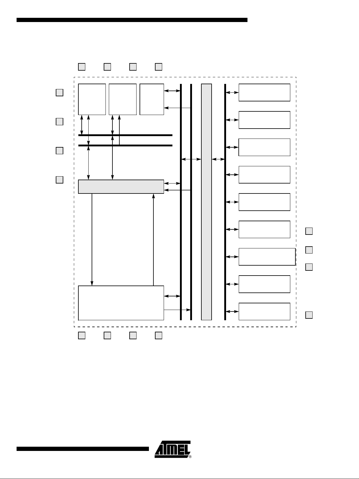
Block Diagram
PSEN#
ALE/PROG#
EA#/VPP
P3(A16) P1(A17)P2(A15-8) P0(AD7-0)
ROM
PORTS 0-3
EPROM
OTPROM
32 KB
16-bit Memory Code
16-bit Memory Address
RAM
1 Kbyte
AT/TSC8x251G2D
Timers 0, 1 and 2
UART
Baud Rate Generator
Event and Waveform
Controller
AWAIT#
Bus Interface Unit
16-bit Instruction Bus
CPU
VDD VSS VSS1
24-bit Program Counter Bus
VSS2
TWI/SPI/mWire
Controller
Watchdog Timer
Peripheral Interface Unit
8-bit Data Bus
24-bit Data Address Bus
8-bit Internal Bus
Power Management
Clock Unit
Clock System Prescaler
Keyboard Interface
Interrupt Handler
Unit
RST
XTAL2
XTAL1
NMI
4135D–8051–08/05
3
Page 4
Pin Description
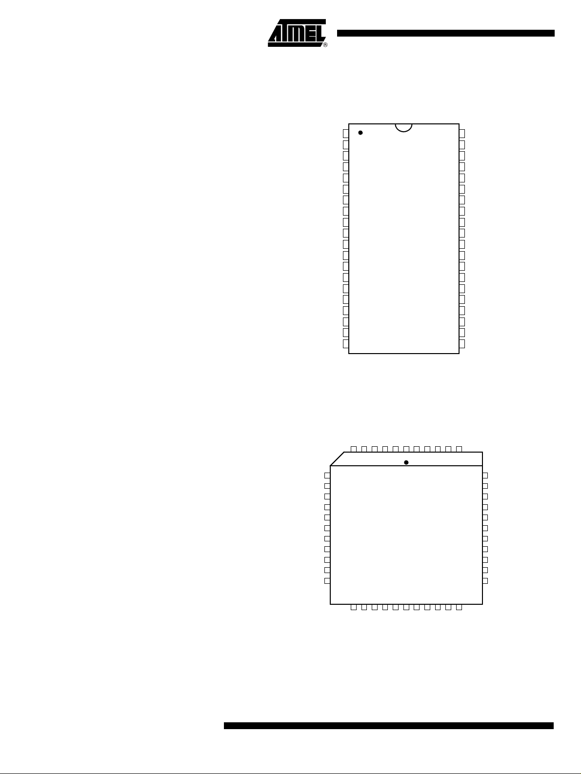
Pinout Figure 1. TSC80251G2D 40-pin DIP package
P1.0/T2 VDD
P1.1/T2EX
P1.2/ECI
P1.3/CEX0
P1.4/CEX1/SS#
P1.6/CEX3/SCL/SCK/WAIT#
P1.7/A17/CEX4/SDA/MOSI/WCLK
P3.0/RXD
P3.1/TXD
P3.2/INT0#
P3.3/INT1#
P3.4/T0
P3.5/T1
P3.7/A16/RD#
XTAL2
XTAL1
1
2
3
4
5
6
7
8
9
RST
10
TSC80251G2D
11
12
13
14
15
16
17
18
19
20
VSS P2.0/A8
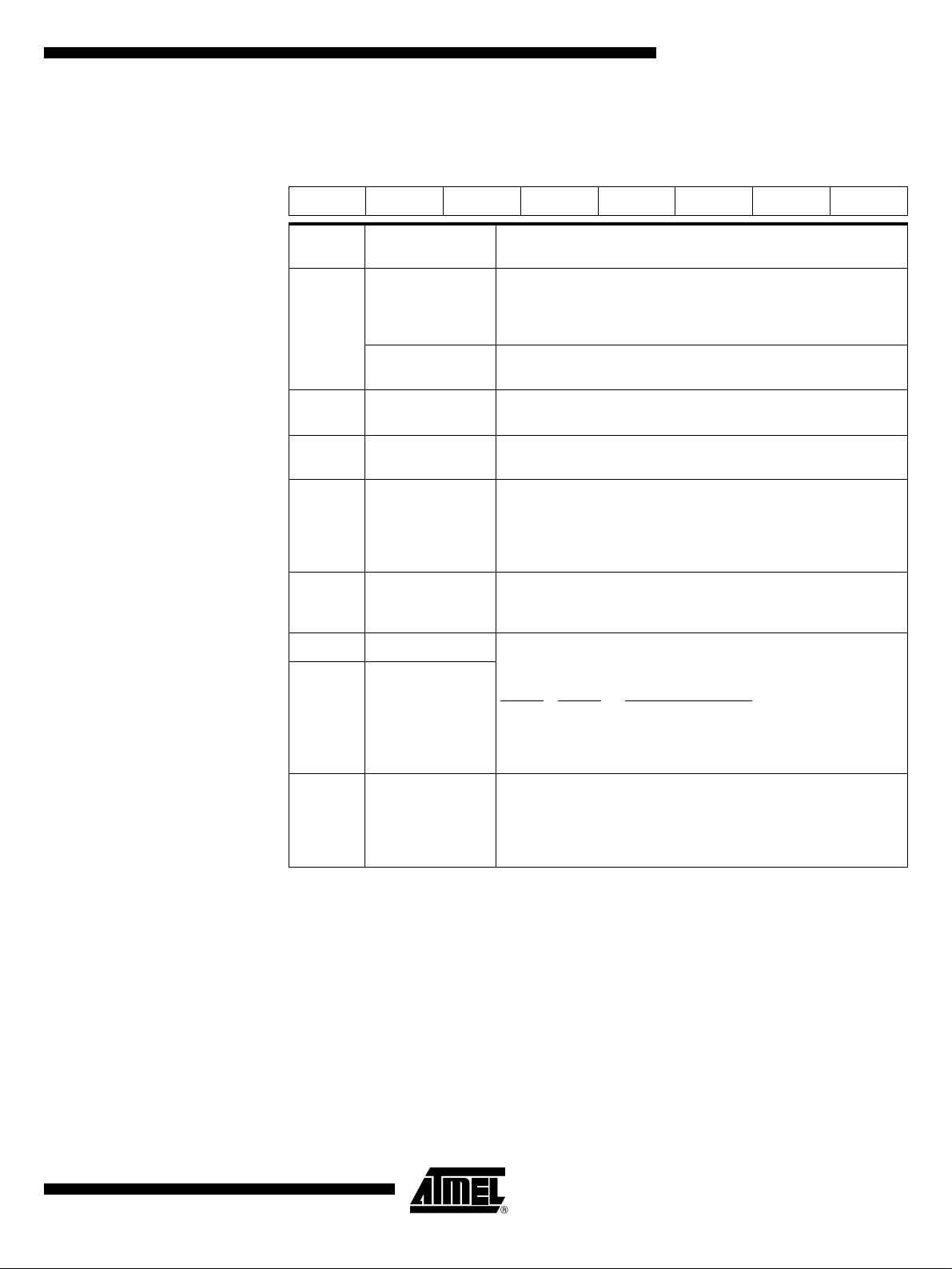
Figure 2. TSC80251G2D 44-pin PLCC Package
40
39
38
37
36
35P1.5/CEX2/MISO
34
33
32
31
30
29
28
27
26
25
24
23
22
21
P0.0/AD0
P0.1/AD1
P0.2/AD2
P0.3/AD3
P0.4/AD4
P0.5/AD5
P0.6/AD6
P0.7/AD7
EA#/VPP
ALE/PROG#
PSEN#
P2.7/A15
P2.6/A14
P2.5/A13
P2.4/A12P3.6/WR#
P2.3/A11
P2.2/A10
P2.1/A9
P1.5/CEX2/MISO
P1.6/CEX3/SCL/SCK/WAIT#
P1.7/A17/CEX4/SDA/MOSI/WCLK
RST
P3.0/RXD
AWAIT#
P3.1/TXD
P3.2/INT0#
P3.3/INT1#
P3.4/T0
P3.5/T1
P1.4/CEX1/SS#
P1.3/CEX0
P1.2/ECI
P1.1/T2EX
P1.0/T2
VSS1
65432
7
8
9
10
11
12
13
14
15
16
17
1819202122232425262728
XTAL2
P3.6/WR#
P3.7/A16/RD#
1
TSC80251G2D
VSS
VSS2
XTAL1
VDD
P0.0/AD0
P0.1/AD1
P0.2/AD2
P0.3/AD3
4443424140
P2.0/A8
P2.1/A9
P2.2/A10
P2.3/A11
P2.4/A12
39
38
37
36
35
34
33
32
31
30
29
P0.4/AD4
P0.5/AD5
P0.6/AD6
P0.7/AD7
EA#/VPP
NMI
ALE/PROG#
PSEN#
P2.7/A15
P2.6/A14
P2.5/A13
4
AT/TSC8x251G2D
4135D–8051–08/05
Page 5
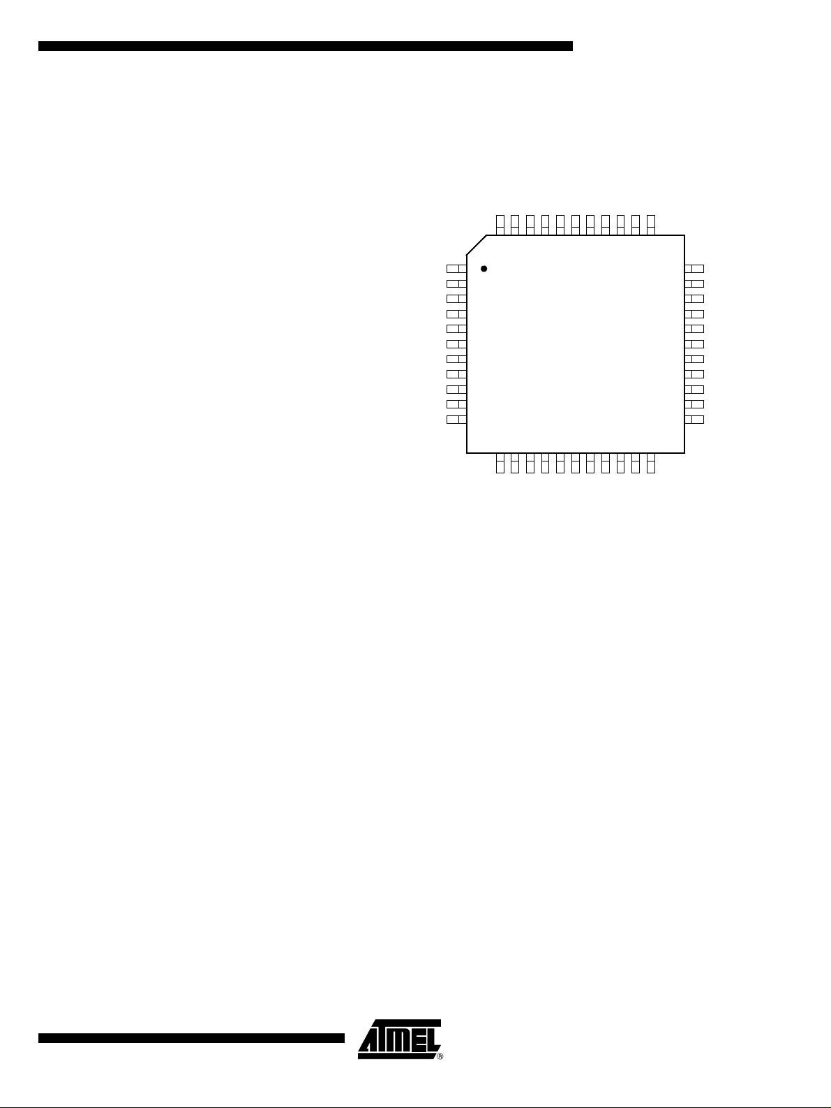
Figure 3. TSC80251G2D 44-pin VQFP Package
P1.4/CEX1/SS#
P1.3/CEX0
P1.2/ECI
4443424140393837363534
P1.5/CEX2/MISO
P1.6/CEX3/SCL/SCK/WAIT#
P1.7/A17/CEX4/SDA/MOSI/WCLK
RST
P3.0/RXD
AWAIT#
P3.1/TXD
P3.2/INT0#
P3.3/INT1#
P3.4/T0
P3.5/T1
1
2
3
4
5
6
7
8
9
10
11
TSC80251G2D
1213141516171819202122
AT/TSC8x251G2D
P1.1/T2EX
P1.0/T2
VSS1
VDD
P0.0/AD0
P0.1/AD1
P0.2/AD2
P0.3/AD3
33
P0.4/AD4
32
P0.5/AD5
31
P0.6/AD6
30
P0.7/AD7
29
EA#/VPP
28
NMI
27
ALE/PROG#
26
PSEN#
25
P2.7/A15
24
P2.6/A14
23
P2.5/A13
XTAL2
P3.6/WR#
P3.7/A16/RD#
VSS
VSS2
XTAL1
P2.0/A8
P2.1/A9
P2.2/A10
P2.3/A11
P2.4/A12
4135D–8051–08/05
5
Page 6

Table 1. TSC80251G2D Pin Assignment
DIP PLCC VQFP Name DIP PLCC VQFP Name
1 39 VSS1 23 17 VSS2
1 2 40 P1.0/T2 21 24 18 P2.0/A8
2 3 41 P1.1/T2EX 22 25 19 P2.1/A9
3 4 42 P1.2/ECI 23 26 20 P2.2/A10
4 5 43 P1.3/CEX0 24 27 21 P2.3/A11
5 6 44 P1.4/CEX1/SS# 25 28 22 P2.4/A12
6 7 1 P1.5/CEX2/MISO 26 29 23 P2.5/A13
7 8 2 P1.6/CEX3/SCL/SCK/WAIT# 27 30 24 P2.6/A14
8 9 3 P1.7/A17/CEX4/SDA/MOSI/WCLK 28 31 25 P2.7/A15
9 10 4 RST 29 32 26 PSEN#
10 11 5 P3.0/RXD 30 33 27 ALE/PROG#
12 6 AWAIT# 34 28 NMI
11 13 7 P3.1/TXD 31 35 29 EA#/VPP
12 14 8 P3.2/INT0# 32 36 30 P0.7/AD7
13 15 9 P3.3/INT1# 33 37 31 P0.6/AD6
14 16 10 P3.4/T0 34 38 32 P0.5/AD5
15 17 11 P3.5/T1 35 39 33 P0.4/AD4
16 18 12 P3.6/WR# 36 40 34 P0.3/AD3
17 19 13 P3.7/A16/RD# 37 41 35 P0.2/AD2
18 20 14 XTAL2 38 42 36 P0.1/AD1
19 21 15 XTAL1 39 43 37 P0.0/AD0
20 22 16 VSS 40 44 38 VDD
6
AT/TSC8x251G2D
4135D–8051–08/05
Page 7
Signals
Table 2. Product Name Signal Description
Signal
Name Type Description
th
18
Address Bit
A17 O
A16 O
Output to memory as 18th external address bit (A17) in extended bus
applications, depending on the values of bits RD0 and RD1 in UCONFIG0
byte (see Table 13, Page 20).
th
17
Address Bit
Output to memory as 17th external address bit (A16) in extended bus
applications, depending on the values of bits RD0 and RD1 in UCONFIG0
byte (see Table 13, Page 20).
AT/TSC8x251G2D
Alternate
Function
P1.7
P3.7
(1)
A15:8
(1)
AD7:0
ALE O
AWAIT# I
CEX4:0 I/O
EA# I
ECI O
I/O
Address Lines
O
Upper address lines for the external bus.
Address/Data Lines
Multiplexed lower address lines and data for the external memory.
Address Latch Enable
ALE signals the start of an external bus cycle and indicates that valid
address information are available on lines A16/A17 and A7:0. An external
latch can use ALE to demultiplex the address from address/data bus.
Real-time Asynchronous Wait States Input
When this pin is active (low level), the memory cycle is stretched until it
becomes high. When using the Product Name as a pin-for-pin replacement
for a 8xC51 product, AWAIT# can be unconnected without loss of
compatibility or power consumption increase (on-chip pull-up).
Not available on DIP package.
PCA Input/Output pins
CEXx are input signals for the PCA capture mode and output signals for
the PCA compare and PWM modes.
External Access Enable
EA# directs program memory accesses to on-chip or off-chip code memory.
For EA# = 0, all program memory accesses are off-chip.
For EA# = 1, an access is on-chip ROM if the address is within the range of
the on-chip ROM; otherwise the access is off-chip. The value of EA# is
latched at reset.
For devices without ROM on-chip, EA# must be strapped to ground.
PCA External Clock input
ECI is the external clock input to the 16-bit PCA timer.
P2.7:0
P0.7:0
–
–
P1.7:3
–
P1.2
4135D–8051–08/05
MISO I/O
MOSI I/O
INT1:0# I
SPI Master Input Slave Output line
When SPI is in master mode, MISO receives data from the slave
peripheral. When SPI is in slave mode, MISO outputs data to the master
controller.
SPI Master Output Slave Input line
When SPI is in master mode, MOSI outputs data to the slave peripheral.
When SPI is in slave mode, MOSI receives data from the master controller.
External Interrupts 0 and 1
INT1#/INT0# inputs set IE1:0 in the TCON register. If bits IT1:0 in the
TCON register are set, bits IE1:0 are set by a falling edge on INT1#/INT0#.
If bits IT1:0 are cleared, bits IE1:0 are set by a low level on INT1#/INT0#.
P1.5
P1.7
P3.3:2
7
Page 8

Table 2. Product Name Signal Description (Continued)
Signal
Name Type Description
Non Maskable Interrupt
Holding this pin high for 24 oscillator periods triggers an interrupt.
NMI I
P0.0:7 I/O
P1.0:7 I/O
When using the Product Name as a pin-for-pin replacement for a 8xC51
product, NMI can be unconnected without loss of compatibility or power
consumption increase (on-chip pull-down).
Not available on DIP package.
Port 0
P0 is an 8-bit open-drain bidirectional I/O port. Port 0 pins that have 1s
written to them float and can be used as high impedance inputs. To avoid
any paraitic current consumption, Floating P0 inputs must be polarized to
V
or VSS.
DD
Port 1
P1 is an 8-bit bidirectional I/O port with internal pull-ups. P1 provides
interrupt capability for a keyboard interface.
Alternate
Function
–
AD7:0
–
P2.0:7 I/O
P3.0:7 I/O
PROG# I
PSEN# O
RD# O
RST I
RXD I/O
Port 2
P2 is an 8-bit bidirectional I/O port with internal pull-ups.
Port 3
P3 is an 8-bit bidirectional I/O port with internal pull-ups.
Programming Pulse input
The programming pulse is applied to this input for programming the on-chip
EPROM/OTPROM.
Program Store Enable/Read signal output
PSEN# is asserted for a memory address range that depends on bits RD0
and RD1 in UCONFIG0 byte (see ).
Read or 17
Read signal output to external data memory depending on the values of
bits RD0 and RD1 in UCONFIG0 byte (see Table 13, Page 20).
Reset input to the chip
Holding this pin high for 64 oscillator periods while the oscillator is running
resets the device. The Port pins are driven to their reset conditions when a
voltage greater than V
This pin has an internal pull-down resistor which allows the device to be
reset by connecting a capacitor between this pin and VDD.
Asserting RST when the chip is in Idle mode or Power-Down mode returns
the chip to normal operation.
Receive Serial Data
RXD sends and receives data in serial I/O mode 0 and receives data in
serial I/O modes 1, 2 and 3.
th
Address Bit (A16)
is applied, whether or not the oscillator is running.
IH1
A15:8
–
–
–
P3.7
–
P3.0
TWI Serial Clock
SCL I/O
SCK I/O
SDA I/O
SS# I
8
AT/TSC8x251G2D
When TWI controller is in master mode, SCL outputs the serial clock to
slave peripherals. When TWI controller is in slave mode, SCL receives
clock from the master controller.
SPI Serial Clock
When SPI is in master mode, SCK outputs clock to the slave peripheral.
When SPI is in slave mode, SCK receives clock from the master controller.
TWI Serial Data
SDA is the bidirectional TWI data line.
SPI Slave Select Input
When in Slave mode, SS# enables the slave mode.
4135D–8051–08/05
P1.6
P1.6
P1.7
P1.4
Page 9

AT/TSC8x251G2D
Table 2. Product Name Signal Description (Continued)
Signal
Name Type Description
Alternate
Function
T1:0 I/O
T2 I/O
T2EX I
TXD O
VDD PWR
VPP I
VSS GND
VSS1 GND
Timer 1:0 External Clock Inputs
When timer 1:0 operates as a counter, a falling edge on the T1:0 pin
increments the count.
Timer 2 Clock Input/Output
For the timer 2 capture mode, T2 is the external clock input. For the Timer 2
clock-out mode, T2 is the clock output.
Timer 2 External Input
In timer 2 capture mode, a falling edge initiates a capture of the timer 2
registers. In auto-reload mode, a falling edge causes the timer 2 register to
be reloaded. In the up-down counter mode, this signal determines the
count direction: 1 = up, 0 = down.
Transmit Serial Data
TXD outputs the shift clock in serial I/O mode 0 and transmits data in serial
I/O modes 1, 2 and 3.
Digital Supply Voltage
Connect this pin to +5V or +3V supply voltage.
Programming Supply Voltage
The programming supply voltage is applied to this input for programming
the on-chip EPROM/OTPROM.
Circuit Ground
Connect this pin to ground.
Secondary Ground 1
This ground is provided to reduce ground bounce and improve power
supply bypassing. Connection of this pin to ground is recommended.
However, when using the TSC80251G2D as a pin-for-pin replacement for a
8xC51 product, VSS1 can be unconnected without loss of compatibility.
Not available on DIP package.
–
P1.0
P1.1
P3.1
–
–
–
–
VSS2 GND
WAIT# I
WCLK O
WR# O
XTAL1 I
Secondary Ground 2
This ground is provided to reduce ground bounce and improve power
supply bypassing. Connection of this pin to ground is recommended.
However, when using the TSC80251G2D as a pin-for-pin replacement for a
8xC51 product, VSS2 can be unconnected without loss of compatibility.
Not available on DIP package.
Real-time Synchronous Wait States Input
The real-time WAIT# input is enabled by setting RTWE bit in WCON
(S:A7h). During bus cycles, the external memory system can signal
‘system ready’ to the microcontroller in real time by controlling the WAIT#
input signal.
Wait Clock Output
The real-time WCLK output is enabled by setting RTWCE bit in WCON
(S:A7h). When enabled, the WCLK output produces a square wave signal
with a period of one half the oscillator frequency.
Write
Write signal output to external memory.
Input to the on-chip inverting oscillator amplifier
To use the internal oscillator, a crystal/resonator circuit is connected to this
pin. If an external oscillator is used, its output is connected to this pin.
XTAL1 is the clock source for internal timing.
–
P1.6
P1.7
P3.6
–
4135D–8051–08/05
9
Page 10

Table 2. Product Name Signal Description (Continued)
Signal
Name Type Description
Alternate
Function
XTAL2 O
Note: The description of A15:8/P2.7:0 and AD7:0/P0 .7:0 are for the Non-Page mo de chip con-
figuration. If the chip is configured in Page mode operation, port 0 carries the lower
address bits (A7:0) while port 2 carries the upper address bits (A15:8) and the data
(D7:0).
Output of the on-chip inverting oscillator amplifier
To use the internal oscillator, a crystal/resonator circuit is connected to this
pin. If an external oscillator is used, leave XTAL2 unconnected.
–
10
AT/TSC8x251G2D
4135D–8051–08/05
Page 11
AT/TSC8x251G2D
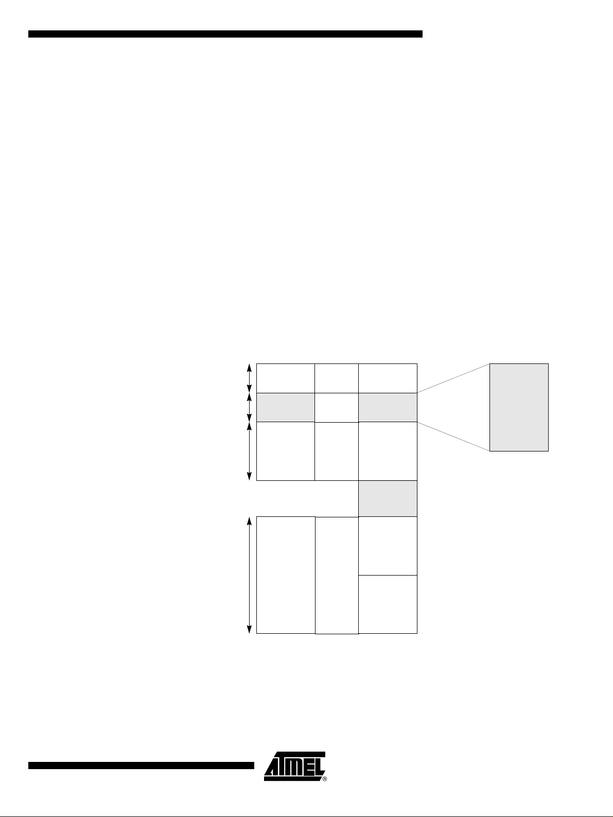
Address Spaces The TSC80251G2D derivatives implement four different address space s:
• On-chip ROM program/code memor y (n ot pr e sen t in ROM le ss de vic es)
• On-chip RAM data memory
• Special Function Registers (SFRs)
• Configuration array
Program/Code Memory The TSC83251G2D and TSC87251G2D implement 32 KB of on-chip program/code
memory. Figure 4 shows the split of the inter nal and external program/code m emory
spaces. If EA# is tied to a high level, the 32-Kbyte on-chip program memory is mapped
in the lower part of segment FF: where the C251 core jumps after reset. The rest of the
program/code memory space is mapped to the external memory. If EA# is tied to a low
level, the internal program/code memory is not used and all the accesses are directed to
the external memory.
The TSC83251G2D products provide the internal program/code memory in a masked
ROM memory while the TSC87251G2D products provide it in an EPROM memory. For
the TSC80251G2D products, there is no internal program/code memory and EA# must
be tied to a low level.
Figure 4. Program/Code Memory Mapping
Program/code
External Memory Space
Program/code
Segments
On-chip ROM/EPROM
Code Memory
32 KB
32 KB
64 KB
128 KB
Note: Special care should be taken when the Program Counter (PC) increments:
If the program executes exclusively from on-chip code memory (not from external memory), beware of executing code from the upper eight bytes of the on-chip ROM
(FF:7FF8h-FF:7FFFh). Because of its pipeline capability, the TSC80251G2D derivative
may attempt to prefetch code from external memory (at an address above FF:7FFFh)
and thereby disrupt I/O Ports 0 and 2. Fetching code constants from these 8 bytes does
not affect Ports 0 and 2.
When PC reaches the end of segment FF:, it loops to the reset address FF:0000h (for
FF:FFFFh
FF:8000h
FF:7FFFh
32 KBEA# = 0 EA# = 1
FF:0000h
FE:FFFFh
FE:0000h
FD:FFFFh
Reserved
02:0000h
01:FFFFh
01:0000h
00:FFFFh
00:0000h
4135D–8051–08/05
11
Page 12
compatibility with the C51 Architecture). When PC increments beyond the end of segment FE:, it continues at the reset address FF:0000h (linearity). When PC increments
beyond the end of segment 01:, it loops to the beginning of segment 00: (this prevents
from its going into the reserved area).
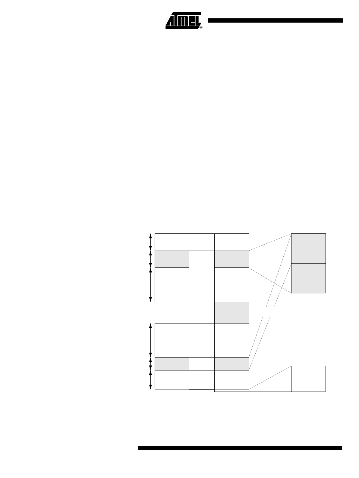
Data Memory The TSC80251G2D derivatives implement 1 Kbyte of on-chip data RAM. Figure 5
shows the split of the internal and external data memory spaces. This memory is
mapped in the data space just over the 32 bytes of registers area (see TSC80251 Programmers’ Guide). Hence, the part of the on-chip RAM located from 20h to FFh is bit
addressable. This on-chip RAM is not accessible through the program/code memory
space.
For faster computation with the on-chip ROM/EPROM code of the
TSC83251G2D/TSC87251G2D, its upper 16 KB are also mapped in the upper part of
the region 00: if the On-Chip Code Memory Map configuration bit is cleared (EMAP# bit
in UCONFIG1 byte, see Figure ). However, if EA# is tied to a low level, the
TSC80251G2D derivative is running as a ROMless product and the code is actually
fetched in the corresponding external memory (i.e. the upper 16 KB of the lower 32 KB
of the segment FF:). If EMAP# bit is set, the on-chip ROM is not accessible through the
region 00:.
All the accesses to the portion of the data space with no on-chip memory mapped onto
are redirected to the external memory.
Figure 5. Data Memory Mapping
Data External
Memory Space
32 KB
32 KB
64 KB
64 KB
16 KB
ª47 KB
EA# = 0 EA# = 1
EMAP# = 1
FF:FFFFh
FF:8000h
FF:7FFFh
FF:0000h
FE:FFFFh
FE:0000h
FD:FFFFh
Reserved
02:0000h
01:FFFFh
01:0000h
00:FFFFh
00:C000h
00:BFFFh
00:0420h
On-chip ROM/EPROM
Code MemoryData Segments
16 KB
16 KB
EMAP# = 0
RAM Data
1 Kbyte
32 bytes reg.
12
AT/TSC8x251G2D
4135D–8051–08/05
Page 13
AT/TSC8x251G2D
Special Function Registers
The Special Function Registers (SFRs) of the TSC80251G2D derivatives fall into the
categories detailed in Table 1 to Table 9.
SFRs are placed in a reserved on-chip memory region S: which is not repre sented in the
data memory mapping (Figure 5). The relative addresses within S: of these SFRs are
provided together with their reset values in Table . They are upward compatible with the
SFRs of the standard 80C51 and the Intel’s 80C251Sx family. In this table, the C251
core registers are identified by Note 1 and are described in the TSC80251 Programmer’s Guide. The other SFRs are described in the TSC80251 G1D De sign Guid e. All the
SFRs are bit-addressable using the C251 instruction set.
Table 1. C251 Core SFRs
Mnemonic Name Mnemonic Name
(1)
ACC
(1)
B
PSW Program Status Word DPH
PSW1 Program Status Word 1
(1)
SP
Accumulator SPH
B Register DPL
DPXL
Stack Pointer - LSB of SPX
(1)
(1)
(1)
(1)
Stack Pointer High - MSB of
SPX
Data Pointer Low byte - LSB of
DPTR
Data Pointer High byte - MSB
of DPTR
Data Pointer Extended Low
byte of DPX - Region number
Note: 1. These SFRs can also be accessed by their corresponding registers in the register
file.
Table 2. I/O Port SFRs
Mnemonic Name Mnemonic Name
P0 Port 0 P2 Port 2
P1 Port 1 P3 Port 3
Table 3. Timers SFRs
Mnemonic Name Mnemonic Name
TL0
TH0
TL1
TH1
TL2
TH2
TCON
Timer/Counter 0 Low
Byte
Timer/Counter 0 High
Byte
Timer/Counter 1 Low
Byte
Timer/Counter 1 High
Byte
Timer/Counter 2 Low
Byte
Timer/Counter 2 High
Byte
Timer/Counter 0 and 1
Control
TMOD
T2CON
T2MOD Timer/Counter 2 Mode
RCAP2L
RCAP2H
WDTRST WatchDog Timer Reset
Timer/Counter 0 and 1
Modes
Timer/Counter 2
Control
Timer/Counter 2
Reload/Capture Low
Byte
Timer/Counter 2
Reload/Capture High
Byte
4135D–8051–08/05
13
Page 14
Table 4. Serial I/O Port SFRs
Mnemonic Name Mnemonic Name
SCON Serial Control SADDR Slave Address
SBUF Serial Data Buffer BRL Baud Rate Reload
SADEN
Slave Address
Mask
BDRCON Baud Rate Control
Table 5. SSLC SFRs
Mnemonic Name Mnemonic Name
SSCON
SSDAT
SSCS
Synchronous Serial
control
Synchronous Serial
Data
Synchronous Serial
Control and Status
SSADR
SSBR
Table 6. Event Waveform Control SFRs
Mnemonic Name Mnemonic Name
CCON EWC-PCA Timer/Counter Control CCAP0L
CMOD EWC-PCA Timer/Counter Mode CCAP1L
CL
EWC-PCA Timer/Counter Low
Register
CCAP2L
EWC-PCA Compare Capture
Module 0 Low Register
EWC-PCA Compare Capture
Module 1 Low Register
EWC-PCA Compare Capture
Module 2 Low Register
Synchronous Serial
Address
Synchronous Serial
Bit Rate
CH
CCAPM0 EWC-PCA Timer/Counter Mode 0 CCAP4L
CCAPM1 EWC-PCA Timer/Counter Mode 1 CCAP0H
CCAPM2 EWC-PCA Timer/Counter Mode 2 CCAP1H
CCAPM3 EWC-PCA Timer/Counter Mode 3 CCAP2H
CCAPM4 EWC-PCA Timer/Counter Mode 4 CCAP3H
EWC-PCA Timer/Counter High
Register
CCAP3L
CCAP4H
EWC-PCA Compare Capture
Module 3 Low Register
EWC-PCA Compare Capture
Module 4 Low Register
EWC-PCA Compare Capture
Module 0 High Register
EWC-PCA Compare Capture
Module 1 High Register
EWC-PCA Compare Capture
Module 2 High Register
EWC-PCA Compare Capture
Module 3 High Register
EWC-PCA Compare Capture
Module 4 High Register
14
AT/TSC8x251G2D
4135D–8051–08/05
Page 15
AT/TSC8x251G2D
Table 7. System Management SFRs
Mnemonic Name Mnemonic Name
PCON Power Control CKRL Clock Reload
POWM Power Management WCON
Synchronous Real-Time Wait State
Control
Table 8. Interrupt SFRs
Mnemonic Name Mnemonic Name
IE0 Interrupt Enable Control 0 IPL0 Interrupt Priority Control Low 0
IE1 Interrupt Enable Control 1 IPH1 Interrupt Priority Control High 1
IPH0 Interrupt Priority Control High 0 IPL1 Interrupt Priority Control Low 1
Table 9. Keyboard Interface SFRs
Mnemonic Name Mnemonic Name
P1IE Port 1 Input Interrupt Enable P1LS Port 1 Level Selection
P1F Port 1 Flag
4135D–8051–08/05
15
Page 16
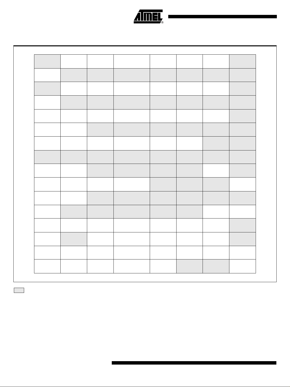
Table 10. SFR Descriptions
0/8 1/9 2/A 3/B 4/C 5/D 6/E 7/F
F8h
F0h
E8h
E0h
D8h
D0h
C8h
C0h
B8h
B0h
A8h
(1)
B
0000 0000
(1)
ACC
0000 0000
CCON
00X0 0000
(1)
PSW
0000 0000
T2CON
0000 0000
IPL0
X000 0000
P3
1111 1111
IE0
0000 0000
CH
0000 0000
CL
0000 0000
CMOD
00XX X000
(1)
PSW1
0000 0000
T2MOD
XXXX XX00
SADEN
0000 0000
IE1
XX0X XXX0
SADDR
0000 0000
CCAP0H
0000 0000
CCAP0L
0000 0000
CCAPM0
X000 0000
RCAP2L
0000 0000
IPL1
XX0X XXX0
CCAP1H
0000 0000
CCAP1L
0000 0000
CCAPM1
X000 0000
RCAP2H
0000 0000
IPH1
XX0X XXX0
CCAP2H
0000 0000
CCAP2L
0000 0000
CCAPM2
X000 0000
TL2
0000 0000
CCAP3H
0000 0000
CCAP3L
0000 0000
CCAPM3
X000 0000
TH2
0000 0000
CCAP4H
0000 0000
CCAP4L
0000 0000
CCAPM4
X000 0000
(1)
SPH
0000 0000
IPH0
X000 0000
FFh
F7h
EFh
E7h
DFh
D7h
CFh
C7h
BFh
B7h
AFh
A0h
98h
90h
88h
80h
P2
1111 1111
SCON
0000 0000
P1
1111 1111
TCON
0000 0000
P0
1111 1111
SBUF
XXXX XXXX
TMOD
0000 0000
(1)
SP
0000 0111
BRL
0000 0000
SSBR
0000 0000
TL0
0000 0000
(1)
DPL
0000 0000
BDRCON
XXX0 0000
(2)
SSCON
TL1
0000 0000
(1)
DPH
0000 0000
P1LS
0000 0000
(3)
SSCS
TH0
0000 0000
(1)
DPXL
0000 0001
P1IE
0000 0000
SSDAT
0000 0000
TH1
0000 0000
WDTRST
1111 1111
0000 0000
SSADR
0000 0000
0000 1000
0/8 1/9 2/A 3/B 4/C 5/D 6/E 7/F
Reserved
Notes: 1. These registers are described in the TSC80251 Programmer’s Guide (C251 core registers).
2. In TWI and SPI modes, SSCON is splitted in two separate registers. SSCON reset value is 0000 0000 in TWI mode and
0000 0100 in SPI mode.
3. In read and write modes, SSCS is splitted in two separate registers. SSCS reset value is 1111 1000 in read mode and 0000
0000 in write mode.
P1F
CKRL
WCON
XXXX XX00
POWM
0XXX XXXX
PCON
0000 0000
A7h
9Fh
97h
8Fh
87h
16
AT/TSC8x251G2D
4135D–8051–08/05
Page 17

AT/TSC8x251G2D
Configuration Bytes The TSC80251G2D derivatives provide user design flexibility by configuring certain
operating features at device reset. These features fall into the following categories:
• external memory interface (Page mode, address bits, programmed wait states and
the address range for RD#, WR#, and PSEN#)
• source mode/binary mode opcodes
• selection of bytes stored on the stack by an interrupt
• mapping of the upper portion of on-chip code memory to region 00:
Two user configuration bytes UCONFIG0 (see Table 11) and UCONFIG1 (see Table
12) provide the information.
When EA# is tied to a low level, the configuration bytes are fetched from the external
address space. The TSC80251G2D derivatives reserve the top eight bytes of the memory address space (FF:FFF8h-FF:FFFFh) for an external 8-byte configuration array.
Only two bytes are actually used: UCONFIG0 at FF:FFF8h and UCONFIG1 at
FF:FFF9h.
For the mask ROM devices, configuration information is stored in on-chip memory (see
ROM Verifying). When EA# is tied to a high level, the configuration information is
retrieved from the on-chip memory instead of the external a ddress space and there is no
restriction in the usage of the external memory.
4135D–8051–08/05
17
Page 18
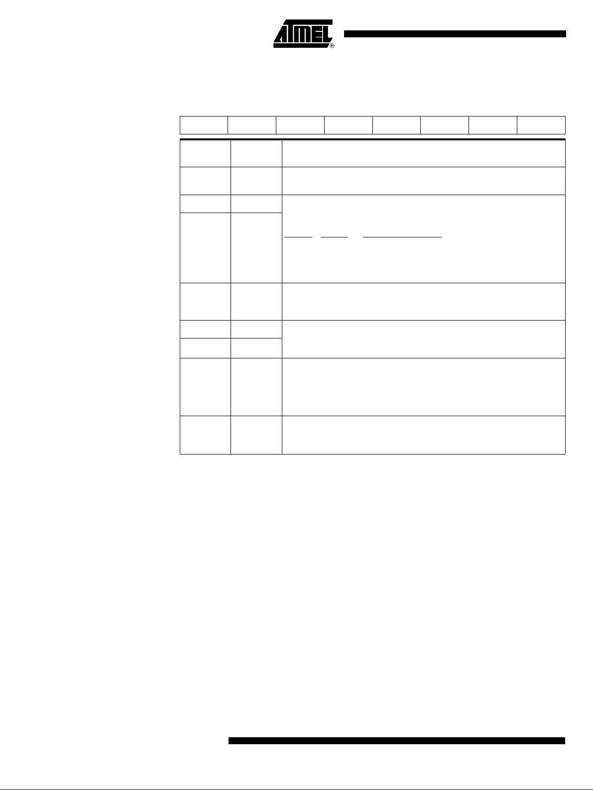
Table 11. Configuration Byte 0
UCONFIG0
76543210
- WSA1# WSA0# XALE# RD1 RD0 PAGE# SRC
Bit Number
7-
6 WSA1# Wait State A bits
5 WSA0#
4 XALE#
3 RD1 Memory Signal Select bits
2 RD0
1 PAGE#
0SRC
Bit
Mnemonic Description
Reserved
Set this bit when writing to UCONFIG0.
Select the number of wait states for RD#, WR# and PSEN# signals for external
memory accesses (all regions except 01:).
WSA1#
WSA0# Number of Wait States
00 3
01 2
10 1
11 0
Extend ALE bit
Clear to extend the duration of the ALE pulse from T
Set to minimize the duration of the ALE pulse to 1·T
Specify a 18-bit, 17-bit or 16-bit external address bus and the usage of RD#,
WR# and PSEN# signals (see Table 13).
Page Mode Select bit
Clear to select the faster Page mode with A15:8/D7:0 on Port 2 and A7:0 on
Port 0.
Set to select the non-Page mode
0.
Source Mode/Binary Mode Select bit
Clear to select the binary mode.
Set to select the source mode.
to 3·T
OSC
OSC
(1)
(2)
with A15:8 on Port 2 and A7:0/D7:0 on Port
OSC.
.
18
Notes: 1. UCONFIG0 is fetched twice so it can be properly read both in Page or Non-Page
modes. If P2.1 is cleared during the first data fetch, a Page mode configuration is
used, otherwise the subsequent fetches are performed in Non-Page mode.
2. This selection provides compatibility with the standard 80C51 hardware which is multiplexing the address LSB and the data on Port 0.
AT/TSC8x251G2D
4135D–8051–08/05
Page 19
AT/TSC8x251G2D
Table 12. Configuration Byte 1
UCONFIG1
76543210
CSIZE - - INTR WSB WSB1# WSB0# EMAP#
Bit
Number Bit Mnemonic Description
On-Chip Code Memory Size bit
CSIZE
TSC87251G2D
7
Clear to select 16 KB of on-chip code memory (TSC87251G1D
product).
Set to select 32 KB of on-chip code memory (TSC87251G2D product).
(1)
TSC80251G2D
TSC83251G2D
6-
5-
4INTR
3WSB
2 WSB1# Wait State B bits
1 WSB0#
0 EMAP#
Reserved
Set this bit when writing to UCONFIG1.
Reserved
Set this bit when writing to UCONFIG1.
Reserved
Set this bit when writing to UCONFIG1.
Interrupt Mode bit
Clear so that the interrupts push two bytes onto the stack (the two lower
bytes of the PC register).
Set so that the interrupts push four bytes onto the stack (the three bytes
of the PC register and the PSW1 register).
Wait State B bit
Clear to generate one wait state for memory region 01:.
Set for no wait states for memory region 01:.
Select the number of wait states for RD#, WR# and PSEN# signals for
external memory accesses (only region 01:).
WSB1#
00 3
01 2
10 1
11 0
On-Chip Code Memory Map bit
Clear to map the upper 16 KB of on-chip code memory (at FF:4000hFF:7FFFh) to the data space (at 00:C000h-00:FFFFh).
Set not to map the upper 16 KB of on-chip code memory (at FF:4000hFF:7FFFh) to the data space.
WSB0# Number of Wait States
(2)
(3)
4135D–8051–08/05
Notes: 1. The CSIZE is only available on EPROM/OTPROM products.
2. Two or four bytes are transparently popped according to INTR when using the RETI
instruction. INTR must be set if interrupts are used with code executing outside
region FF:.
3. Use only for Step A compatibility; set this bit when WSB1:0# are used.
19
Page 20

Configuration Byte 1 Table 13. Address Ranges and Usage of RD#, WR# and PSEN# Signals
RD1 RD0 P1.7 P3.7/RD# PSEN# WR#
External
Memory
00A17A16
0 1 I/O pin A16
1 0 I/O pin I/O pin
Read
1 1 I/O pin
signal for
regions 00:
and 01:
Read signal for all
external memory
locations
Read signal for all
external memory
locations
Read signal for all
external memory
locations
Read signal for
regions FE: and FF:
Write signal for all
external memory
locations
Write signal for all
external memory
locations
Write signal for all
external memory
locations
Write signal for all
external memory
locations
256 KB
128 KB
64 KB
2 × 64 KB
(1)
Notes: 1. This selection provides compatibility with the standard 80C51 hardware which has
separate external memory spaces for data and code.
20
AT/TSC8x251G2D
4135D–8051–08/05
Page 21
AT/TSC8x251G2D
Instruction Set Summary
This section contains tables that summarize the instruction set. For each instruction
there is a short description, its length in bytes, and its execution time in states (one sta te
time is equal to two system clock cycles). There are two concurrent processes limiting
the effective instruction throughput:
• Instruction Fetch
• Instruction Execution
Table 20 to Table 32 assume code executing from on-chip memory, then the CPU is
fetching 16-bit at a time and this is never limiting the execution speed.
If the code is fetched from external memory, a pre-fetch queue will store instructions
ahead of execution to optimize the memory bandwidth usage when slower instructions
are executed. However, the effective speed may be limited depending on the average
size of instructions (for the considered section of the progra m flow). The ma ximum ave rage instruction throughput is provided by Table 14 depending on the external memory
configuration (from Page Mode to Non-Page Mode and the maximum number of wait
states). If the average size of instructions is not an integer, the maximum effective
throughput is found by pondering the number of states for the neighbor integer values.
Table 14. Minimum Number of States per Instruction for given Average Sizes
Average size
of Instructions
(bytes)
1123456
Page Mode
(states)
0 Wait
State
1 Wait
Non-page Mode (states)
State 2 Wait States 3 Wait States 4 Wait States
Notation for Instruction Operands
224681012
3 3 6 9 12 15 18
4 4 812162024
5 5 10 15 20 25 30
If the average execution time of the considered instructions is larger than the number of
states given by Table 14, this larger value will prevail as the limiting factor. Otherwise,
the value from Table 14 must be taken. This is providing a fair estimation of the execution speed but only the actual code execution can provide the final value.
Table 15 to Table 19 provide notation for Instruction Operands.
Table 15. Notation for Direct Addressing
Direct
Address Description C251 C51
dir8
dir16
A direct 8-bit address. This can be a memory address (00h-7Fh) or a
SFR address (80h-FFh). It is a byte (default), word or double word
depending on the other operand.
A 16-bit memory address (00:0000h-00:FFFFh) used in direct
addressing.
33
3–
4135D–8051–08/05
21
Page 22
Table 16. Notation for Immediate Addressing
Immediate
Address Description C251 C51
#data An 8-bit constant that is immediately addressed in an instruction 3 3
#data16 A 16-bit constant that is immediately addressed in an instruction 3 –
#0data16
#1data16
#short
A 32-bit constant that is immediately addressed in an instruction. The
upper word is filled with zeros (#0data16) or ones (#1data16).
A constant, equal to 1, 2, or 4, that is immediately addressed in an
instruction.
3–
3–
Table 17. Notation for Bit Addressing
Direct
Address Description C251 C51
A directly addressed bit (bit number = 00h-FFh) in memory or an
SFR. Bits 00h-7Fh are the 128 bits in byte locations 20h-2Fh in the
bit51
bit
on-chip RAM. Bits 80h-FFh are the 128 bits in the 16 SFRs with
addresses that end in 0h or 8h, S:80h, S:88h, S:90h,..., S:F0h,
S:F8h.
A directly addressed bit in memory locations 00:0020h-00:007Fh or
in any defined SFR.
–
3
Table 18. Notation for Destination in Control Instructions
Direct
Address Description C251 C51
rel
addr11
A signed (two’s complement) 8-bit relative address. The destination
is -128 to +127 bytes relative to the next instruction’s first byte.
An 11-bit target address. The target is in the same 2-Kbyte block of
memory as the next instruction’s first byte.
33
–3
3
22
addr16
addr24
AT/TSC8x251G2D
A 16-bit target address. The target can be anywhere within the same
64-Kbyte region as the next instruction’s first byte.
A 24-bit target address. The target can be anywhere within the 16Mbyte address space.
–3
3–
4135D–8051–08/05
Page 23

AT/TSC8x251G2D
Table 19. Notation for Register Operands
Register Description C251 C51
at Ri
Rn
n
Rm
Rmd
Rms
m, md, ms
WRj
WRjd
WRjs
at WRj
at WRj +dis16
j, jd, js
DRk
DRkd
DRks
at DRk
at DRk +dis16
k, kd, ks
A memory location (00h-FFh) addressed indirectly via byte registers
R0 or R1
Byte register R0-R7 of the currently selected register bank
Byte register index: n = 0-7
Byte register R0-R15 of the currently selected register file
Destination register
Source register
Byte register index: m, md, ms = 0-15
Word register WR0, WR2, ..., WR30 of the currently selected register
file
Destination register
Source register
A memory location (00:0000h-00:FFFFh) addressed indirectly
through word register WR0-WR30, is the target address for jump
instructions.
A memory location (00:0000h-00:FFFFh) addressed indirectly
through word register (WR0-WR30) + 16-bit signed (two’s
complement) displacement value
Word register index: j, jd, js = 0-30
Dword register DR0, DR4, ..., DR28, DR56, DR60 of the currently
selected register file
Destination register
Source register
A memory location (00:0000h-FF:FFFFh) addressed indirectly
through dword register DR0-DR28, DR56 and DR60, is the target
address for jump instruction
A memory location (00:0000h-FF:FFFFh) addressed indirectly
through dword register (DR0-DR28, DR56, DR60) + 16-bit (two’s
complement) signed displacement value
Dword register index: k, kd, ks = 0, 4, 8..., 28, 56, 60
–3
–3
3
3
3
–
–
–
4135D–8051–08/05
23
Page 24

Size and Execution Time for Instruction Families
Table 20. Summary of Add and Subtract Instructions
AddADD <dest>, <src>dest opnd ← dest opnd + src opnd
SubtractSUB <dest>, <src>dest opnd ← dest opnd - src opnd
Add with CarryADDC <dest>, <src>(A) ← (A) + src opnd + (CY)
Subtract with BorrowSUBB <dest>, <src>(A) ← (A) - src opnd - (CY)
<dest>,
Mnemonic
ADD
(1)
<src>
A, Rn Register to ACC 1 1 2 2
A, dir8 Direct address to ACC 2 1
A, at Ri Indirect address to ACC 1 2 2 3
A, #data Immediate data to ACC 2 1 2 1
Rmd, Rms Byte register to/from byte register 3 2 2 1
WRjd, WRjs Word register to/from word register 3 3 2 2
DRkd, DRks Dword register to/from dword register 3 5 2 4
Rm, #data
WRj, #data16
DRk,
#0data16
Comments
Immediate 8-bit data to/from byte
register
Immediate 16-bit data to/from word
register
16-bit unsigned immediate data
to/from dword register
Binary Mode Source Mode
Bytes States Bytes States
(2)
21
(2)
4 332
5 443
5 645
ADD/SUB
Rm, dir8
WRj, dir8
Rm, dir16
WRj, dir16
Rm, at WRj
Rm, at DRk
Direct address (on-chip RAM or SFR)
to/from byte register
Direct address (on-chip RAM or SFR)
to/from word register
Direct address (64K) to/from byte
register
Direct address (64K) to/from word
register
Indirect address (64K) to/from byte
register
Indirect address (16M) to/from byte
register
43
4 433
53
54
43
44
A, Rn Register to/from ACC with carry 1 1 2 2
A, dir8
Direct address (on-chip RAM or SFR)
to/from ACC with carry
21
ADDC/SU
BB
A, at Ri
A, #data
Indirect address to/from ACC with
carry
Immediate data to/from ACC with
carry
1 223
2 121
Notes: 1. A shaded cell denotes an instruction in the C51 Architecture.
2. If this instruction addresses an I/O Port (Px, x = 0-3), add 1 to the number of states.
Add 2 if it addresses a Peripheral SFR.
3. If this instruction addresses external memory location, add N+2 to the number of
states (N: number of wait states).
(2)
(3)
(4)
(3)
(3)
(2)
32
42
43
32
33
21
(2)
(3)
(4)
(3)
(3)
(2)
24
AT/TSC8x251G2D
4135D–8051–08/05
Page 25

AT/TSC8x251G2D
4. If this instruction addresses external memory location, add 2(N+2) to the number of
states (N: number of wait states).
Table 21. Summary of Increment and Decrement Instructions
IncrementINC <dest>dest opnd ← dest opnd + 1
IncrementINC <dest>, <src>dest opnd ← dest opnd + src opnd
DecrementDEC <dest>dest opnd ← dest opnd - 1
DecrementDEC <dest>, <src>dest opnd ← dest opnd - src opnd
<dest>,
Mnemonic
INC
DEC
INC
DEC
INC DRk, #short Double w o rd register by 1, 2, or 4 3 4 2 3
DEC DRk, #short Double word register by 1, 2, or 4 3 5 2 4
INC DPTR Data pointer by 1 1 1 1 1
(1)
<src>
A ACC by 1 1 1 1 1
Rn Register by 1 1 1 2 2
dir8
at Ri Indirect address by 1 1 3 2 4
Rm, #short Byte register by 1, 2, or 4 3 2 2 1
WRj, #short Word register by 1, 2, or 4 3 2 2 1
Comments
Direct address (on-chip RAM or
SFR) by 1
Binary Mode Source Mode
Bytes States Bytes States
22
(2)
22
Notes: 1. A shaded cell denotes an instruction in the C51 Architecture.
2. If this instruction addresses an I/O Port (Px, x = 0-3), add 2 to the number of states.
Add 3 if it addresses a Peripheral SFR.
(2)
4135D–8051–08/05
25
Page 26

Table 22. Summary of Compare Instructions
CompareCMP <dest>, <src>dest opnd - src opnd
Mnemonic
CMP
<dest>,
(2)
<src>
Rmd, Rms Register with register 3 2 2 1
WRjd,
WRjs
DRkd,
DRks
Rm, #data Register with immediate data 4 3 3 2
WRj,
#data16
DRk,
#0data16
DRk,
#1data16
Rm, dir8
WRj, dir8
Rm, dir16 Direct address (64K) with byte register 5 3
WRj, dir16 Direct address (64K) with word register 5 4
Rm, at WRj Indirect address (64K) with byte register 4 3
Rm, at DRk Indirect address (16M) with byte register 4 4
Comments
Word register with word register 3 3 2 2
Dword register with dword register 3 5 2 4
Word register with immediate 16-bit data 5 4 4 3
Dword register with zero-extended 16-bit
immediate data
Dword register with one-extended 16-bit
immediate data
Direct address (on-chip RAM or SFR) with
byte register
Direct address (on-chip RAM or SFR) with
word register
Binary Mode Source Mode
Bytes States Bytes States
5645
5645
43
4433
(1)
(2)
(3)
(2)
(2)
32
42
43
32
33
(1)
(2)
(3)
(2)
(2)
26
Notes: 1. If this instruction addresses an I/O Port (Px, x = 0-3), add 1 to the number of states.
Add 2 if it addresses a Peripheral SFR.
2. If this instruction addresses external memory location, add N+2 to the number of
states (N: number of wait states).
3. If this instruction addresses external memory location, add 2(N+2) to the number of
states (N: number of wait states).
AT/TSC8x251G2D
4135D–8051–08/05
Page 27

AT/TSC8x251G2D
Logical AND
Logical OR
Logical Exclusive OR
Clear
Complement
Rotate LeftRL A(A)
Rotate Left CarryRLC A(A)
Rotate RightRR A(A)
Rotate Right CarryRRC A(A)
(1)
ANL <dest>, <src>dest opnd ← dest opnd Λ src opnd
(1)
ORL <dest>, <src>dest opnd ← dest opnd ς src opnd
(1)
(1)
CLR A(A) ← 0
(1)
(A)
← (A)
0
(CY) ← (A)
(A)0 ← (CY)
(A)
← (A)
7
(CY) ← (A)
(A)7 ← (CY)
XRL <dest>, <src>dest opnd ← dest opnd ∀ src opnd
CPL A(A) ← ∅ (A)
← (A)n, n = 0..6
n+1
7
← (A)n, n = 0..6
n+1
7
← (A)n, n = 7..1
n-1
0
← (A)n, n = 7..1
n-1
0
Mnemonic <dest>, <src>
A, Rn register to ACC 1 1 2 2
A, dir8 Direct address (on-chip RAM or SFR) to ACC 2 1
A, at Ri Indirect address to ACC 1 2 2 3
A, #data Immediate data to ACC 2 1 2 1
dir8, A ACC to direct address 2 2
dir8, #data Immediate 8-bit data to direct address 3 3
(1)
Comments
Binary Mode Source Mode
Bytes States Bytes States
(3)
(4)
(4)
21
22
33
(3)
(4)
(4)
Rmd, Rms Byte register to byte register 3 2 2 1
WRjd, WRjs Word register to word register 3 3 2 2
ANL
ORL
XRL
Rm, #data Immediate 8-bit data to byte register 4 3 3 2
WRj, #data16 Immediate 16-bit data to word register 5 4 4 3
Rm, dir8
WRj, dir8
Direct address (on-chip RAM or SFR) to byte
register
Direct address (on-chip RAM or SFR) to word
register
43
4433
Rm, dir16 Direct address (64K) to byte register 5 3
WRj, dir16 Direct address (64K) to word register 5 4
Rm, at WRj Indirect address (64K) to byte register 4 3
Rm, at DRk Indirect address (16M) to byte register 4 4
(3)
(5)
(6)
(5)
(5)
32
42
43
32
33
CLR A Clear ACC 1 1 1 1
CPL A Complement ACC 1 1 1 1
RL A Rotate ACC left 1 1 1 1
RLC A Rotate ACC left through CY 1 1 1 1
RR A Rotate ACC right 1 1 1 1
(3)
(5)
(6)
(5)
(5)
RRC A Rotate ACC right through CY 1 1 1 1
4135D–8051–08/05
27
Page 28

Notes: 1. Logical instructions that affect a bit are in Table 27.
2. A shaded cell denotes an instruction in the C51 Architecture.
3. If this instruction addresses an I/O Port (Px, x = 0-3), add 1 to the number of states. Add 2 if it addresses a Peripheral SFR.
4. If this instruction addresses an I/O Port (Px, x = 0-3), add 2 to the number of states. Add 3 if it addresses a Peripheral SFR.
5. If this instruction addresses external memory location, add N+2 to the number of states (N: number of wait states).
6. If this instruction addresses external memory location, add 2(N+2) to the number of states (N: number of wait states).
Table 23. Summary of Logical Instructions (2/2)
Shift Left LogicalSLL <dest><dest>0 ← 0
<dest>
(CY) ← <dest>
Shift Right ArithmeticSRA <dest><dest>
<dest>
(CY) ← <dest>
Shift Right LogicalSRL <dest><dest>
<dest>
(CY) ← <dest>
SwapSWAP AA
Mnemonic
← <dest>n, n = 0..msb-1
n+1
msb
← <dest>n, n = msb..1
n-1
0
← <dest>n, n = msb..1
n-1
0
A
3:0
7:4
<dest>,
<src>
(1)
msb
← 0
msb
Comments
← <dest>
msb
Binary Mode Source Mode
Bytes States Bytes States
Rm
Shift byte register left through the
MSB
3221
SLL
WRj
Shift word register left through the
MSB
3221
Rm Shift byte register right 3 2 2 1
SRA
WRj Shift word register right 3 2 2 1
Rm Shift byte register left 3 2 2 1
SRL
WRj Shift word register left 3 2 2 1
SWAP A Swap nibbles within ACC 1 2 1 2
Note: 1. A shaded cell denotes an instruction in the C51 Architecture.
28
AT/TSC8x251G2D
4135D–8051–08/05
Page 29

AT/TSC8x251G2D
Table 24. Summary of Multiply, Divide and Decimal-adjust Instructions
MultiplyMUL AB(B:A) ← (A)×(B)
MUL <dest>, <src>extended dest opnd ← dest opnd × src opnd
DivideDIV AB(A) ← Quotient ((A) ⁄ (B))
(B) ← Remainder ((A) ⁄ (B))
DivideDIV <dest>, <src>ext. dest opnd high ← Quotient (dest opnd ⁄ src opnd)
ext. dest opnd low ← Remainder (dest opnd ⁄ src opnd)
Decimal-adjust ACCDA AIF [[(A)
for Addition (BCD) THEN (A)
IF [[(A)
THEN (A)
Mnemonic
> 9] ∨ [(CY) = 1]]
7:4
← (A)
7:4
<dest>,
(1)
<src>
AB Multiply A and B 1 5 1 5
> 9] ∨ [(AC) = 1]]
3:0
← (A)
3:0
+ 6
7:4
Comments
+ 6 !affects CY;
3:0
Binary Mode Source Mode
Bytes States Bytes States
MUL
DIV
DA A Decimal adjust ACC 1 1 1 1
Rmd, Rms Multiply byte register and byte register 3 6 2 5
WRjd, WRjs Multiply word register and word register 3 12 2 11
AB Divide A and B 1 10 1 10
Rmd, Rms Divide byte register and byte register 3 11 2 10
WRjd, WRjs Divide word register and word register 3 21 2 20
Note: 1. A shaded cell denotes an instruction in the C51 Architecture.
4135D–8051–08/05
29
Page 30

Table 25. Summary of Move Instructions (1/3)
Move to High wordMOVH <dest>, <src>dest opnd
Move with Sign extensionMOVS <dest>, <src>dest opnd ← src opnd with sign extend
Move with Zero extensionMOVZ <dest>, <src>dest opnd ← src opnd with zero extend
Move CodeMOVC A, <src>(A) ← src opnd
Move eXtendedMOVX <dest>, <src>dest opnd ← src opnd
← src opnd
31:16
<dest>,
Mnemonic
<src>
(2)
MOVH DRk, #data16
MOVS WRj, Rm
MOVZ WRj, Rm
A, at A +DPTR
MOVC
Comments
16-bit immediate data into upper
word of dword register
Byte register to word register with
sign extension
Byte register to word register with
zeros extension
Code byte relative to DPTR to
ACC
Binary Mode Source Mode
Bytes States Bytes States
5342
3221
3221
16
A, at A +PC Code byte relative to PC to ACC 1 6
A, at Ri
A, at DPTR
Extended memory (8-bit address)
(2)
to ACC
Extended memory (16-bit
address) to ACC
(2)
1415
13
MOVX
at Ri, A
at DPTR, A
ACC to extended memory (8-bit
address)
ACC to extended memory (16-bit
address)
(2)
(2)
1414
14
Notes: 1. A shaded cell denotes an instruction in the C51 Architecture.
2. Extended memory addressed is in the region specified by DPXL (reset value = 01h).
3. If this instruction addresses external memory location, add N+1 to the number of
states (N: number of wait states).
4. If this instruction addresses external memory location, add N+2 to the number of
states (N: number of wait states).
(3)
(3)
(4)
(3)
16
16
13
14
(3)
(3)
(4)
(3)
30
AT/TSC8x251G2D
4135D–8051–08/05
Page 31

Table 26. Summary of Move Instructions (2/3)
(1)
Move
MOV <dest>, <src>dest opnd ← src opnd
AT/TSC8x251G2D
Mnemonic
MOV
<dest>,
(2)
<src>
Comments
Binary Mode Source Mode
Bytes States Bytes States
A, Rn Register to ACC 1 1 2 2
A, dir8
Direct address (on-chip RAM or SFR)
to ACC
21
(3)
21
A, at Ri Indirect address to ACC 1 2 2 3
A, #data Immediate data to ACC 2 1 2 1
Rn, A ACC to register 1 1 2 2
Rn, dir8
Direct address (on-chip RAM or SFR)
to register
21
(3)
32
Rn, #data Immediate data to register 2 1 3 2
dir8, A
dir8, Rn
dir8, dir8
dir8, at Ri
ACC to direct address (on-chip RAM or
SFR)
Register to direct address (on-chip
RAM or SFR)
Direct address to direct address (onchip RAM or SFR)
Indirect address to direct address (onchip RAM or SFR)
22
22
33
23
(3)
(3)
(4)
(3)
22
33
33
34
(3)
(3)
(3)
(3)
(4)
(3)
dir8, #data
Immediate data to direct address (onchip RAM or SFR)
at Ri, A ACC to indirect address 1 3 2 4
at Ri, dir8
Direct address (on-chip RAM or SFR)
to indirect address
at Ri, #data Immediate data to indirect address 2 3 3 4
DPTR,
#data16
Load Data Pointer with a 16-bit
constant
Notes: 1. Instructions that move bits are in Table 27.
2. Move instructions from the C51 Architecture.
3. If this instruction addresses an I/O Port (Px, x = 0-3), add 1 to the number of states.
Add 2 if it addresses a Peripheral SFR.
4. Apply note 3 for each dir8 operand.
33
23
(3)
(3)
33
34
(3)
(3)
3232
4135D–8051–08/05
31
Page 32

(1)
Move
MOV <dest>, <src>dest opnd ← src opnd
Binary Mode Source Mode
(1)
Mnemonic <dest>, <src>
Comments
MOV Rmd, Rms Byte register to byte register 3 2 2 1
MOV WRjd, WRjs Word register to word register 3 2 2 1
MOV DRkd, DRks Dword register to dword register 3 3 2 2
MOV Rm, #data Immediate 8-bit data to byte register 4 3 3 2
MOV WRj, #data16 Immediate 16-bit data to word register 5 3 4 2
MOV DRk, #0data16 zero-ext 16bit immediate data to dword register 5 5 4 4
MOV DRk, #1data16 one-ext 16bit immediate data to dword register 5 5 4 4
MOV Rm, dir8 Direct address (on-chip RAM or SFR) to byte register 4 3
MOV WRj, dir8 Direct address (on-chip RAM or SFR) to word register 4 4 3 3
MOV DRk, dir8 Direct address (on-chip RAM or SFR) to dword register 4 6 3 5
MOV Rm, dir16 Direct address (64K) to byte register 5 3
MOV WRj, dir16 Direct address (64K) to word register 5 4
MOV DRk, dir16 Direct address (64K) to dword register 5 6
MOV Rm, at WRj Indirect address (64K) to byte register 4 3
MOV Rm, at DRk Indirect address (16M) to byte register 4 4
MOV WRjd, at WRjs Indirect address (64K) to word register 4 4
MOV WRj, at DRk Indirect address (16M) to word register 4 5
MOV dir8, Rm Byte register to direct address (on-chip RAM or SFR) 4 4
Bytes States Bytes States
(3)
(4)
(5)
(6)
(4)
(4)
(5)
(5)
(3)
32
42
43
45
32
33
33
34
33
(3)
(4)
(5)
(6)
(4)
(4)
(5)
(5)
(3)
MOV dir8, WRj Word register to direct address (on-chip RAM or SFR) 4 5 3 4
MOV dir8, DRk Dword register to direct address (on-chip RAM or SFR) 4 7 3 6
MOV dir16, Rm Byte register to direct address (64K) 5 4
MOV dir16, WRj Word register to direct address (64K) 5 5
MOV dir16, DRk Dword register to direct address (64K) 5 7
MOV at WRj, Rm Byte register to indirect address (64K) 4 4
MOV at DRk, Rm Byte register to indirect address (16M) 4 5
MOV at WRjd, WRjs Word register to indirect address (64K) 4 5
MOV at DRk, WRj Word register to indirect address (16M) 4 6
32
MOV
MOV
MOV
Rm, at WRj
+dis16
WRj, at WRj
+dis16
Rm, at DRk
+dis24
AT/TSC8x251G2D
Indirect with 16-bit displacement (64K) to byte register 5 6
Indirect with 16-bit displacement (64K) to word register 5 7
Indirect with 16-bit displacement (16M) to byte register 5 7
(4)
(5)
(6)
(4)
(4)
(5)
(5)
(4)
(5)
(4)
43
44
46
33
34
34
35
45
46
46
(4)
(5)
(6)
(4)
(4)
(5)
(5)
(4)
(5)
(4)
4135D–8051–08/05
Page 33
AT/TSC8x251G2D
MOV
MOV
MOV
MOV
MOV
WRj, at WRj
+dis24
at WRj +dis16,
Rm
at WRj +dis16,
WRj
at DRk +dis24,
Rm
at DRk +dis24,
WRj
Indirect with 16-bit displacement (16M) to word register 5 8
Byte register to indirect with 16-bit displacement (64K) 5 6
Word register to indirect with 16-bit displacement (64K) 5 7
Byte register to indirect with 16-bit displacement (16M) 5 7
Word register to indirect with 16-bit displacement (16M) 5 8
Notes: 1. Instructions that move bits are in Table27.
2. Move instructions unique to the C251 Architecture.
3. If this instruction addresses an I/O Port (Px, x = 0-3), add 1 to the number of states. Add 2 if it addresses a Peripheral SFR.
4. If this instruction addresses external memory location, add N+2 to the number of states (N: number of wait states).
5. If this instruction addresses external memory location, add 2(N+1) to the number of states (N: number of wait states).
6. If this instruction addresses external memory location, add 4(N+2) to the number of states (N: number of wait states).
(5)
(4)
(5)
(4)
(5)
47
45
46
46
47
(5)
(4)
(5)
(4)
(5)
4135D–8051–08/05
33
Page 34

Table 27. Summary of Bit Instructions
Clear BitCLR <dest>dest opnd ← 0
Set BitSETB <dest>dest opnd ← 1
Complement BitCPL <dest>dest opnd ← ∅ bit
AND Carry with BitANL CY, <src>(CY) ← (CY) ∧ src opnd
AND Carry with Complement of BitANL CY, /<src>(CY) ← (CY) ∧ ∅ src opnd
OR Carry with BitORL CY, <src>(CY) ← (CY) ∨ src opnd
OR Carry with Complement of BitORL CY, /<src>(CY) ← (CY) ∨ ∅ src opnd
Move Bit to CarryMOV CY, <src>(CY) ← src opnd
Move Bit from CarryMOV <dest>, CYdest opnd ← (CY)
Mnemonic
CLR
SETB
CPL
ANL
<dest>,
(1)
<src>
Comments
Binary Mode Source Mode
Bytes States Bytes States
CY Clear carry 1 1 1 1
bit51 Clear direct bit 2 2
bit Clear direct bit 4 4
(3)
(3)
22
33
CY Set carry 1 1 1 1
bit51 Set direct bit 2 2
bit Set direct bit 4 4
(3)
(3)
22
33
CY Complement carry 1 1 1 1
bit51 Complement direct bit 2 2
bit Complement direct bit 4 4
CY, bit51 And direct bit to carry 2 1
CY, bit And direct bit to carry 4 3
CY, /bit51
CY, /bit
And complemented direct bit to
carry
And complemented direct bit to
carry
21
43
CY, bit51 Or direct bit to carry 2 1
CY, bit Or direct bit to carry 4 3
(3)
(3)
(2)
(2)
(2)
(2)
(2)
(2)
22
33
21
32
21
32
21
32
(3)
(3)
(3)
(3)
(3)
(3)
(2)
(2)
(2)
(2)
(2)
(2)
34
ORL
MOV
Notes: 1. A shaded cell denotes an instruction in the C51 Architecture.
AT/TSC8x251G2D
CY, /bit51
CY, /bit
Or complemented direct bit to
carry
Or complemented direct bit to
carry
21
43
CY, bit51 Move direct bit to carry 2 1
CY, bit Move direct bit to carry 4 3
bit51, CY Move carry to direct bit 2 2
bit, CY Move carry to direct bit 4 4
(2)
(2)
(2)
(2)
(3)
(3)
21
32
21
32
22
33
(2)
(2)
(2)
(2)
(3)
(3)
2. If this instruction addresses an I/O Port (Px, x = 0-3), add 1 to the number of states.
Add 2 if it addresses a Peripheral SFR.
3. If this instruction addresses an I/O Port (Px, x = 0-3), add 2 to the number of states.
Add 3 if it addresses a Peripheral SFR.
4135D–8051–08/05
Page 35

AT/TSC8x251G2D
Table 28. Summary of Exchange, Push and Pop Instructions
Exchange bytesXCH A, <src>(A) ↔ src opnd
Exchange DigitXCHD A, <src>(A)
PushPUSH <src>(SP) ← (SP) +1; ((SP)) ← src opnd;
(SP) ← (SP) + size (src opnd) - 1
PopPOP <dest>(SP) ← (SP) - size (dest opnd) + 1;
dest opnd ← ((SP)); (SP) ← (SP) -1
↔ src opnd
3:0
3:0
Mnemonic
XCH
XCHD A, at Ri
PUSH
POP
<dest>,
<src>
A, Rn ACC and register 1 3 2 4
A, dir8
A, at Ri ACC and indirect address 1 4 2 5
dir8 Push direct address onto stack 2 2
#data Push immediate data onto stack 4 4 3 3
#data16
Rm Push byte register onto stack 3 4 2 3
WRj Push word register onto stack 3 5 2 4
DRk
dir8
Rm Pop byte register from stack 3 3 2 2
WRj Pop word register from stack 3 5 2 4
Binary Mode Source Mode
(1)
Comments
ACC and direct address (on-chip
RAM or SFR)
ACC low nibble and indirect address
(256 bytes)
Push 16-bit immediate data onto
stack
Push double word register onto
stack
Pop direct address (on-chip RAM or
SFR) from stack
Bytes States Bytes States
23
1425
5545
3928
23
(3)
(2)
(2)
23
22
23
(3)
(2)
(2)
4135D–8051–08/05
DRk Pop double word register from stack 3 9 2 8
Notes: 1. A shaded cell denotes an instruction in the C51 Architecture.
2. If this instruction addresses an I/O Port (Px, x = 0-3), add 1 to the number of states.
Add 2 if it addresses a Peripheral SFR.
3. If this instruction addresses an I/O Port (Px, x = 0-3), add 2 to the number of states.
Add 3 if it addresses a Peripheral SFR.
35
Page 36

Table 29. Summary of Conditional Jump Instructions (1/2)
Jump conditional on statusJcc rel(PC) ← (PC) + size (instr);
IF [cc] THEN (PC) ← (PC) + rel
Binary Mode Source Mode
Bytes States Bytes States
Mnemonic
<dest>,
<src>
(1)
Comments
JC rel Jump if carry 2 1/4
JNC rel Jump if not carry 2 1/4
JE rel Jump if equal 3 2/5
JNE rel Jump if not equal 3 2/5
JG rel Jump if greater than 3 2/5
JLE rel Jump if less than, or equal 3 2/5
JSL rel Jump if less than (signed) 3 2/5
JSLE rel Jump if less than, or equal (signed) 3 2/5
JSG rel Jump if greater than (signed) 3 2/5
JSGE rel Jump if greater than or equal (signed) 3 2/5
Notes: 1. A shaded cell denotes an instruction in the C51 Architecture.
2. States are given as jump not-taken/taken.
3. In internal execution only, add 1 to the number of states of the ‘jump taken’ if the destination address is internal and odd.
(3)
(3)
(3)
(3)
(3)
(3)
(3)
(3)
(3)
(3)
21/4
21/4
21/4
21/4
21/4
21/4
21/4
21/4
21/4
21/4
(3)
(3)
(3)
(3)
(3)
(3)
(3)
(3)
(3)
(3)
36
AT/TSC8x251G2D
4135D–8051–08/05
Page 37

AT/TSC8x251G2D
Table 30. Summary of Conditional Jump Instructions (2/2)
Jump if bitJB <src>, rel(PC) ← (PC) + size (instr);
IF [src opnd = 1] THEN (PC) ← (PC) + rel
Jump if not bitJNB <src>, rel(PC) ← (PC) + size (instr);
IF [src opnd = 0] THEN (PC) ← (PC) + rel
Jump if bit and clearJBC <dest>, rel(PC) ← (PC) + size (instr);
IF [dest opnd = 1] THEN
dest opnd ← 0
(PC) ← (PC) + rel
Jump if accumulator is zeroJZ rel(PC) ← (PC) + size (instr);
IF [(A) = 0] THEN (PC) ← (PC) + rel
Jump if accumulator is not zeroJNZ rel(PC) ← (PC) + size (instr);
IF [(A) ≠ 0] THEN (PC) ← (PC) + rel
Compare and jump if not equalCJNE <src1>, <src2>, rel(PC) ← (PC) + size (instr);
IF [src opnd1 < src opnd2] THEN (CY) ← 1
IF [src opnd1 ≥ src opnd2] THEN (CY) ← 0
IF [src opnd1 ≠ src opnd2] THEN (PC) ← (PC) + rel
Decrement and jump if not zeroDJNZ <dest>, rel(PC) ← (PC) + size (instr); dest opnd ← dest opnd -1;
IF [ϕ (Z)] THEN (PC) ← (PC) + rel
(2)
(3)(6)
(3)(6)
(3)(6)
(3)(6)
(5)(6)
(5)(
6)
(6)
(6)
Source Mode
32/5
43/6
32/5
43/6
34/7
46/9
22/5
22/5
Binary Mode
Mnemonic <dest>, <src>
(1)
Comments
Bytes States Bytes States
bit51, rel Jump if direct bit is set 3 2/5
JB
bit, rel
Jump if direct bit of 8-bit address
location is set
54/7
bit51, rel Jump if direct bit is not set 3 2/5
JNB
bit, rel
Jump if direct bit of 8-bit address
location is not set
54/7
bit51, rel Jump if direct bit is set & clear bit 3 4/7
JBC
bit, rel
Jump if direct bit of 8-bit address
location is set and clear
7/10
5
JZ rel Jump if ACC is zero 2 2/5
JNZ rel Jump if ACC is not zero 2 2/5
(2)
(3)(6)
(3)(6)
(3)(6)
(3)
(5)(6)
(5)(6)
(6)
(6)
4135D–8051–08/05
A, dir8, rel
A, #data, rel
Compare direct address to ACC and
jump if not equal
Compare immediate to ACC and
jump if not equal
32/5
32/5
CJNE
Rn, #data, rel
at Ri, #data, rel
Rn, rel
Compare immediate to register and
jump if not equal
Compare immediate to indirect and
jump if not equal
Decrement register and jump if not
zero
32/5
33/6
22/5
DJNZ
dir8, rel
Decrement direct address and jump
if not zero
33/6
Notes: 1. A shaded cell denotes an instruction in the C51 Architecture.
2. States are given as jump not-taken/taken.
3. If this instruction addresses an I/O Port (Px, x = 0-3), add 1 to the number of states.
Add 2 if it addresses a Peripheral SFR.
4. If this instruction addresses an I/O Port (Px, x = 0-3), add 2 to the number of states.
(3)(6)
(6)
(6)
(6)
(6)
(4)(6)
32/5
32/5
43/6
44/7
33/6
33/6
(3)(6)
(6)
(6)
(6)
(6)
(4)(6)
37
Page 38

Add 3 if it addresses a Peripheral SFR.
5. If this instruction addresses an I/O Port (Px, x = 0-3), add 3 to the number of states.
Add 5 if it addresses a Peripheral SFR.
6. In internal execution only, add 1 to the number of states of the ‘jump taken’ if the destination address is internal and odd.
Table 31. Summary of Unconditional Jump Instructions
Absolute jumpAJMP <src>(PC) ← (PC) +2; (PC)
Extended jumpEJMP <src>(PC) ← (PC) + size (instr); (PC)
Long jumpLJMP <src>(PC) ← (PC) + size (instr); (PC)
Short jumpSJMP rel(PC) ← (PC) +2; (PC) ← (PC) +rel
Jump indirectJMP at A +DPTR(PC)
← FFh; (PC)
23:16
No operationNOP(PC) ← (PC) +1
← src opnd
10:0
15:0
15:0
← src opnd
23:0
← src opnd
← (A) + (DPTR)
<dest>,
Mnemonic
<src>
(1)
Comments
AJMP addr11 Absolute jump 2 3
addr24 Extended jump 5 6
EJMP
at DRk Extended jump (indirect) 3 7
at WRj Long jump (indirect) 3 6
LJMP
addr16 Long jump (direct address) 3 5
SJMP rel Short jump (relative address) 2 4
JMP at A +DPTR Jump indirect relative to the DPTR 1 5
Binary Mode Source Mode
Bytes States Bytes States
(2)(3)
(2)(4)
(2)(4)
(2)(4)
(2)(4)
(2)(4)
(2)(4)
23
45
26
25
35
24
15
NOP No operation (Jump never) 1 1 1 1
Notes: 1. A shaded cell denotes an instruction in the C51 Architecture.
2. In internal execution only, add 1 to the number of states if the destination address is
internal and odd.
3. Add 2 to the number of states if the destination address is external.
4. Add 3 to the number of states if the destination address is external.
(2)(3)
(2)(4)
(2)(4)
(2)(4)
(2)(4)
(2)(4)
(2)(4)
38
AT/TSC8x251G2D
4135D–8051–08/05
Page 39

AT/TSC8x251G2D
Table 32. Summary of Call and Return Instructions
Absolute callACALL <src>(PC) ← (PC) +2; push (PC)
(PC)
← src opnd
10:0
Extended callECALL <src>(PC) ← (PC) + size (instr); push (PC)
(PC)
← src opnd
23:0
Long callLCALL <src>(PC) ← (PC) + size (instr); push (PC)
(PC)
← src opnd
15:0
Return from subroutineRETpop (PC)
Extended return from subroutineERETpop (PC)
15:0
23:0
Return from interruptRETIIF [INTR = 0] THEN pop (PC)
IF [INTR = 1] THEN pop (PC)
; pop (PSW1)
23:0
Trap interruptTRAP(PC) ← (PC) + size (instr);
IF [INTR = 0] THEN push (PC)
IF [INTR = 1] THEN push (PSW1); push (PC)
<dest>,
Mnemonic
<src>
(1)
15:0
Comments
ACALL addr11 Absolute subroutine call 2 9
at DRk Extended subroutine call (indirect) 3 14
ECALL
addr24 Extended subroutine call 5 14
at WRj Long subroutine call (indirect) 3 10
LCALL
addr16 Long subroutine call 3 9
RET Return from subroutine 1 7
ERET Exte nded subroutine return 3 9
RETI Return from interrupt 1 7
TRAP Jump to the trap interrupt vector 2 12
23:0
15:0
15:0
;
;
23:0
;
15:0
Binary Mode Source Mode
Bytes States Bytes States
(2)(3)
(2)(3)
(2)(3)
(2)(3)
(2)(3)
(2)
(2)
(2)(4)
(4)
29
213
413
29
39
17
28
17
111
(2)(3)
(2)(3)
(2)(3)
(2)(3)
(2)(3)
(2)
(2)
(2)(4)
(4)
Notes: 1. A shaded cell denotes an instruction in the C51 Architecture.
2. In internal execution only, add 1 to the number of states if the destination/return
address is internal and odd.
3. Add 2 to the number of states if the destination address is external.
4. Add 5 to the number of states if INTR = 1.
4135D–8051–08/05
39
Page 40

Programming and Verifying Non-volatile Memory
Internal Features The internal non-volatile memory of the TSC80251G2D derivatives contains five differ-
ent areas:
• Code Memory
• Configuration Bytes
•Lock Bits
• Encryption Array
• Signature Bytes
EPROM/OTPROM Devices All the internal non-volatile memory but the Signature Bytes of the TSC87251G2D prod-
ucts is made of EPROM cells. The Signature Bytes of the TSC87251G2D products are
made of Mask ROM.
The TSC87251G2D products are programmed and verified in the same manner as
Atmel’s TSC87251G1A, using a SINGLE-PULSE algorithm, which programs at
V
= 12.75V using only one 100µs pulse per byte. This results in a programming time
PP
of less than 10 seconds for the 32 kilobytes on-chip code memory.
The EPROM of the TSC87251G2D products in Window package is erasable by Ultra-
Violet radiation
reprogramming. The quartz window must be covered with an opaque label
(1)
(UV). UV erasure set all the EPROM memory cells to one and allows
(2)
when the
device is in operation. This is not so much to protect the EPROM array from inadvertent
erasure, as to protect the RAM and other on-chip logic. Allowing light to impinge on the
silicon die during device operation may cause a logical malfunction.
The TSC87251G2D products in plastic packages are One Time Programmable (OTP).
An EPROM cell cannot be reset by UV once programmed to zero.
Notes: 1. The recommended erasure procedure is exposure to ultra -violet light (at 2537 Å) to
an integrated dose of at least 20 W-sec/cm
lamp of 12000 µW/cm2 rating for 30 minutes should be sufficient.
2. Erasure of the EPROM begins to occur when the chip is exposed to light wavelength
shorter than 4000 Å. Since sunlight and fluorescent light have wavelength in this
range, exposure to these light sources over an extended time (1 week in sunlight or 3
years in room-level fluorescent lighting) could cause inadvertent erasure.
2
. Exposing the EPROM to an ultra-violet
Mask ROM Devices All the internal non-volatile me mory of TSC83251G2D products is mad e of Mask ROM
cells. They can only be verified by the user, using the same algorithm as the
EPROM/OTPROM devices.
ROMless Devices The TSC80251G2D products do not include on-chip Configuration Bytes, Code Memory
and Encryption Array. They only include Signature Bytes made of Mask ROM cells
which can be read using the same algorithm as the EPROM/OTPROM devices.
Security Features In some microcontroller applications, it is desirable that the user’s program code be
secured from unauthorized access. The TSC83251G2D and TSC87251G2D offer two
kinds of protection for program code stored in the on-chip array:
• Program code in the on-chip Code Memory is encrypted when read out for
verification if the Encryption Array isprogrammed.
• A three-level lock bit system restricts external access to the on-chip code memory.
40
AT/TSC8x251G2D
4135D–8051–08/05
Page 41

AT/TSC8x251G2D
Lock Bit System The TSC87251G2D products implement 3 levels of security for User’s prog ram as
described in Table 33. The TSC83251G2D pro ducts implement only the first level of
security.
Level 0 is the level of an erased part and does not enable any security features.
Level 1 locks the programming of the User’s internal Code Memory, the Configuration
Bytes and the Encryption Array.
Level 2 locks the verifying of the User’s internal Code Memory. It is always possible to
verify the Configuration Bytes and the Lock Bits. It is not possible to verify the Encryption Array.
Level 3 locks the external execution.
Table 33. Lock Bits Programming
External
Level
0 000 Enable Enable Enable
1 001 Enable Enable Enable
2 01x
31xx
Lock bits
LB[2:0]
(3)
(3)
Internal
Execution
Enable Enable Disable Disable Disable
Enable Disable Disable Disable Disable
External
Execution Verification Programming
(1)
(1)
Enable Enable
Disable Disable
PROM read
(MOVC)
(2)
Notes: 1. Returns encrypted data if Encryption Array is programmed.
2. Returns non encrypted data.
3. x means don’t care. Level 2 always enables level 1, and level 3 always enables levels
1 and 2.
The security level may be verified according to Table 34.
Table 34. Lock Bits Verifying
Level Lock bits Data
0 xxxxx000
1 xxxxx001
2 xxxxx01x
3 xxxxx1xx
Note: 1. x means don’t care.
(1)
Encryption Array The TSC83251G2D and TSC8 7251G2D products include a 128-b yte Encryption Array
located in non-volatile memory outside the memory address space. During verification
of the on-chip code memory, the seven low-order address bits also address the Encryption Array. As the byte of the code memory is read, it is exclusive-NOR’ed (XNOR) with
the key byte from the Encryption Array. If the Encryption Array is not programmed (still
all 1s), the user program code is placed on the data b us in its original, unencrypted form.
If the Encryption Array is programmed with key bytes, the user program code is
encrypted and cannot be used without knowledge of the key byte sequence.
4135D–8051–08/05
41
Page 42

To preserve the secrecy of the encryption key byte sequence, the Encryption Array can
not be verified.
Notes: 1. When a MOVC instruction is executed, the content of the ROM is not encrypted. In
order to fully protect the user program code, the lock bit level 1 (see Table 33) must
always be set when encryption is used.
2. If the encryption feature is implemented, the portion of the on-chip code memory that
does not contain program code should be filled with “random” byte values to prevent
the encryption key sequence from being revealed.
Signature Bytes The TSC80251G2D derivatives contain factory-programmed Signature Bytes. These
bytes are located in non-volatile memory outside the memory address space at 30h,
31h, 60h and 61h. To read the Signature Bytes, pe rform the procedure d escribed in section Verify Algorithm, using the verify signature mode (see Table 37). Signature byte
values are listed in Table 35.
Table 35. Signature Bytes (Electronic ID)
Signature Address Signature Data
Vendor Atmel 30h 58h
Architecture C251 31h 40h
Memory
Revision
32 kilobytes EPROM or
OTPROM
32 kilobytes MaskROM
or ROMless
TSC80251G2D
derivative
60h
61h FDh
F7h
77h
Programming Algorithm Figure 6 shows the hardware setup needed to program the TSC87251G2D
EPROM/OTPROM areas:
• The chip has to be put under reset and maintained in this state until completion of
the programming sequence.
• PSEN# and the other control signals (ALE and Port 0) have to be set to a high level.
• Then PSEN# has to be to forced to a low level after two clock cycles or more and it
has to be maintained in this st ate until the completion o f the progra mming sequence
(see below).
• The voltage on the EA# pin must be set to V
• The programming mode is selected according to the code applied on Port 0 (see
Table 36). It has to be applied until the completion of this programming operation.
• The programming address is applied on Ports 1 and 3 which are respectively the
Most Significant Byte (MSB) and the Least Significant Byte (LSB) of the address.
• The programming data are applied on Port 2.
• The EPROM Programming is done by raising the voltage on the EA# pin to V
then by generating a low level pulse on ALE/PROG# pin.
• The voltage on the EA# pin must be lowered to V
programming operation.
• It is possible to alternate programming and verifying operation (See Paragraph
Verify Algorithm). Please make sure the voltage on the EA# pin has actually been
lowered to V
before performing the verifying operation.
DD
DD
.
before completing the
DD
PP
,
42
AT/TSC8x251G2D
4135D–8051–08/05
Page 43

AT/TSC8x251G2D
• PSEN# and the other control signals have to be released to complete a sequence of
programming operations or a sequence of programming and verifying operations.
Figure 6. Setup for Programming
VDD
VDD
VPP
100 ms pulses
Mode
A[7:0]
A[14:8]
Data
Table 36. Programming Modes
ROM Area
On-chip Code
Memory
Configuration
Bytes
(1)
RST EA#/VPP
1V
1V
PP
PP
RST
EA#/VPP
ALE/PROG#
PSEN#
VDD
TSC87251G2D
P0[7:0]
P3[7:0]
P1[7:0]
P2[7:0]
PSEN
VSS/VSS1/VSS2
# ALE/PROG#
01 Pulse68hData
01 Pulse69hData
XTAL1
(2)
4 to 12 MHz
P0 P2 P1(MSB) P3(LSB)
16-bit Address
0000h-7FFFh (32
kilobytes)
CONFIG0: FFF8h
CONFIG1: FFF9h
LB0: 0001h
Lock Bits 1 V
Encryption Array 1 V
PP
PP
0 1 Pulse 6Bh X
0 1 Pulse 6Ch Data 0000h-007Fh
LB1: 0002h
LB2: 0003h
Notes: 1. Signature Bytes are not user-programmable.
2. The ALE/PROG# pulse waveform is shown in Figure 23 page 59.
Verify Algorithm Figure 7 shows the hardware setup needed to verify the TSC87251G2D
EPROM/OTPROM or TSC83251G2D ROM areas:
• The chip has to be put under reset and maintained in this state until the completion
of the verifying sequence.
• PSEN# and the other control signals (ALE and Port 0) have to be set to a high level.
• Then PSEN# has to be to forced to a low level after two clock cycles or more and it
has to be maintained in this state until the completion of the verifying sequence (see
below).
• The voltage on the EA# pin must be set to V
• The Verifyin g M ode is sele cted accordin g to th e code a pplied on Por t 0. It has to be
applied until the completion of this verifying operation.
• The verifying address is applied on Ports 1 and 3 which are respectively the MSB
and the LSB of the address.
and ALE must be set to a high level.
DD
4135D–8051–08/05
43
Page 44

• Then device is driving the data on Port 2.
• It is possible to alternate programming and verification operation (see Paragraph
Programming Algorithm). Please make sure the voltage on the EA# pin has actually
been lowered to V
before performing the verifying operation.
DD
• PSEN# and the other control signals have to be released to complete a sequence of
verifying operations or a sequence of programming and verifying operations.
Table 37. Verifying Modes
ROM Area
(1)
RST EA#/VPP PSEN# ALE/PROG# P0 P2 P1(MSB) P3(LSB)
On-chip code
memory
Configuration Bytes 1 1 0 1 29h Data
Lock Bits 1 1 0 1 2Bh Data 0000h
Signature Bytes 1 1 0 1 29h Data
1 1 0 1 28h Data
16-bit Address
0000h-7FFFh (32
kilobytes)
CONFIG0: FFF8h
CONFIG1: FFF9h
0030h, 0031h, 0060h,
0061h
Notes: 1. To preserve the secrecy of on-chip code memory when encrypted, the Encryption
Array can not be verified.
Figure 7. Setup for Verifying
VDD
RST
EA#/VPP
ALE/PROG#
PSEN#
VDD
VDD
TSC8x251G2D
Mode
A[7:0]
P0[7:0]
P3[7:0]
P2[7:0] Data
44
AT/TSC8x251G2D
A[14:8]
P1[7:0]
XTAL1
VSS/VSS1/VSS2
4 to 12 MHz
4135D–8051–08/05
Page 45

AT/TSC8x251G2D
AC Characteristics - Commercial & Industrial
AC Characteristics - External Bus Cycles
Definition of Symbols Table 38 . External Bus Cycles Timing Symbol Definitions
Signals Conditions
A Address H High
D Data In L Low
L ALE V Valid
Q Data Out X No Longer Valid
R RD#/PSEN# Z Floating
WWR#
Timings Test conditions: capacitive load on all pins = 50 pF.
Table 39 and Table 40 list the AC timing parameters for the TSC80251G2D derivatives
with no wait states. External wait states can be added by extending PSEN#/RD#/WR#
and or by extending ALE. In these tables, Note 2 marks paramete rs affected by one AL E
wait state, and Note 3 marks parameters affected by PSEN#/RD#/WR# wait states.
Figure 8 to Figure 13 show the bus cycles with the timing parameters.
4135D–8051–08/05
45
Page 46

Table 39. Bus Cycles AC Timings; VDD = 4.5 to 5.5 V, TA = -40 to 85°C
12 MHz 16 MHz 24 MHz
Symbol Parameter
T
1/F
T
T
T
T
T
T
T
T
T
T
OSC
T
LHLL
T
AVLL
T
LLAX
RLRH
WLWH
LLRL
T
LHAX
RLDV
RHDX
RHAX
RLAZ
RHDZ1
RHDZ2
RHLH1
OSC
ALE Pulse Width 78 58 38 ns
Address Valid to ALE Low 78 58 37 ns
Address hold after ALE Low 19 11 3 ns
(1)
RD#/PSEN# Pulse Width 162 121 78 ns
WR# Pulse Width 165 124 81 ns
(1)
ALE Low to RD#/PSEN# Low 22 14 6 ns
ALE High to Address Hold 99 70 40 ns
(1)
RD#/PSEN# Low to Valid Data 146 104 61 ns
(1)
Data Hold After RD#/PSEN# High 0 0 0 ns
Address Hold After RD#/PSEN#
(1)
High
(1)
RD#/PSEN# Low to Address Float 0 0 0 ns
Instruction Float After RD#/PSEN#
High
Data Float After RD#/PSEN# High 215 165 115 ns
RD#/PSEN# high to ALE High
(Instruction)
UnitMin Max Min Max Min Max
83 62 41 ns
(2)
(2)
(3)
(3)
(2)
(3)
000ns
45 40 30 ns
49 43 31 ns
T
T
T
T
T
T
T
AVRL
T
T
T
T
T
RD#/PSEN# high to ALE High
RHLH2
(Data)
WR# High to ALE High 215 169 115 ns
WHLH
Address (P0) Valid to Valid Data In 250 175 105 ns
AVDV1
Address (P2) Valid to Valid Data In 306 223 140 ns
AVDV2
Address (P0) Valid to Valid
AVDV3
Instruction In
Data Hold after Address Hold 0 0 0 ns
AXDX
(1)
Address Valid to RD# Low 100 70 40 ns
Address (P0) Valid to WR# Low 100 70 40 ns
AVWL1
Address (P2) Valid to WR# Low 158 115 74 ns
AVWL2
Data Hold after WR# High 90 69 32 ns
WHQX
Data Valid to WR# High 133 102 72 ns
QVWH
WR# High to Address Hold 167 125 84 ns
WHAX
215 169 115 ns
150 109 68 ns
Notes: 1. Specification for PSEN# are identical to those for RD#.
2. If a wait state is added by extending ALE, add 2·T
OSC.
3. If wait states are added by extending RD#/PSEN#/WR#, add 2N·T
(N = 1..3).
OSC
(2)(3)
(2)(3)
(3)
(2)
(2)
(2)
(3)
46
AT/TSC8x251G2D
4135D–8051–08/05
Page 47

AT/TSC8x251G2D
Table 40. Bus Cycles AC Timings; VDD = 2.7 to 5.5 V, TA = -40 to 85°C
12 MHz 16 MHz
Symbol Parameter
T
T
T
T
T
T
T
T
T
T
T
T
T
T
T
T
T
T
T
T
T
T
T
T
OSC
T
LHLL
T
AVLL
T
LLAX
RLRH
WLWH
LLRL
LHAX
RLDV
RHDX
RHAX
RLAZ
RHDZ1
RHDZ2
RHLH1
RHLH2
WHLH
AVDV1
AVDV2
AVDV3
AXDX
AVRL
AVWL1
AVWL2
WHQX
QVWH
WHAX
1/F
OSC
ALE Pulse Width 72 52 ns
Address Valid to ALE Low 71 51 ns
Address hold after ALE Low 14 6 ns
(1)
RD#/PSEN# Pulse Width 163 121 ns
WR# Pulse Width 165 124 ns
(1)
ALE Low to RD#/PSEN# Low 17 11 ns
ALE High to Address Hold 90 57 ns
(1)
RD#/PSEN# Low to Valid Data 133 92 ns
(1)
Data Hold After RD#/PSEN# High 0 0 ns
(1)
Address Hold After RD#/PSEN# High 0 0 ns
(1)
RD#/PSEN# Low to Address Float 0 0 ns
Instruction Float After RD#/PSEN# High 59 48 ns
Data Float After RD#/PSEN# High 225 175 ns
RD#/PSEN# high to ALE High (Instruction) 60 47 ns
RD#/PSEN# high to ALE High (Data) 226 172 ns
WR# High to ALE High 226 172 ns
Address (P0) Valid to Valid Data In 289 160 ns
Address (P2) Valid to Valid Data In 296 211 ns
Address (P0) Valid to Valid Instruction In 144 98 ns
Data Hold after Address Hold 0 0 ns
(1)
Address Valid to RD# Low 111 64 ns
Address (P0) Valid to WR# Low 111 64 ns
Address (P2) Valid to WR# Low 158 116 ns
Data Hold after WR# High 82 66 ns
Data Valid to WR# High 135 103 ns
WR# High to Address Hold 168 125 ns
83 62 ns
Notes: 1. Specification for PSEN# are identical to those for RD#.
2. If a wait state is added by extending ALE, add 2·T
OSC.
3. If wait states are added by extending RD#/PSEN#/WR#, add 2N·T
(N = 1..3).
OSC
UnitMin Max Min Max
(2)
(2)
(3)
(3)
(2)
(3)
(2)(3)
(2)(3)
(3)
(2)
(2)
(2)
(3)
4135D–8051–08/05
47
Page 48

Waveforms in Non-Page Mode Figure 8. External Bus Cycle: Code Fetch (Non-Page Mode)
ALE
TLHLL(1)
TLLRL(1) TRHLH1
TRLRH(1)
PSEN#
TRLDV(1)
T
RLAZ
(1)
P0
P2/A16/A17
T
(1)
T
AVLL
T
LHAX
T
LLAX
A7:0 D7:0
(1)
T
AVRL
AVDV2
T
AVDV1
(1)
(1)
A15:8/A16/A17
T
RHDZ1
T
RHDX
Instruction In
T
RHAX
Note: 1. The value of this parameter depends on wait states. See Table 39 and Table 40.
Figure 9. External Bus Cycle: Data Read (Non-Page Mode)
ALE
TLHLL(1)
TLLRL(1) TRHLH2
TRLRH(1)
RD#/PSEN#
TRLDV(1)
T
RLAZ
(1)
P0
P2/A16/A17
T
LHAX
(1)
T
AVLL
T
T
AVDV2
AVRL
T
T
(1)
AVDV1
(1)
LLAX
(1)
A15:8/A16/A17
T
RHDZ2
T
RHDX
D7:0A7:0
Data In
T
RHAX
Note: 1. The value of this parameter depends on wait states. See Table 39 and Table 40.
48
AT/TSC8x251G2D
4135D–8051–08/05
Page 49

AT/TSC8x251G2D
Figure 10. External Bus Cycle: Data Write (Non-Page Mode)
ALE
TLHLL(1)
TWLWH(1)
WR#
(1)
T
P0
P2/A16/A17
TAVLL(1)
T
AVWL1
T
AVWL2
LHAX
T
LLAX
A7:0 D7:0
(1)
(1)
A15:8/A16/A17
T
QVWH
Note: 1. The value of this parameter depends on wait states. See Table 39 and Table 40.
Waveforms in Page Mode Figure 11. External Bus Cycle: Code Fetch (Page Mode)
ALE
PSEN#
P2
P0/A16/A17
(3)
TLHLL(1)
T
TAVLL(1)
T
A7:0/A16/A17
Page Miss(2)
LHAX
T
AVRL
AVDV2
TLLRL(1)
T
RLAZ
(1)
T
LLAX
(1)
(1)
T
AVDV1
(1)
TRLDV(1)
D7:0 D7:0A15:8
Instruction In Instruction In
T
AXDX
T
WHQX
Data Out
T
WHAX
T
AVDV3
T
WHLH
T
RHDZ1
T
RHDX
(1)
A7:0/A16/A17
Page Hit(2)
T
RHAX
4135D–8051–08/05
Note: 1. The value of this parameter depends on wait states. See Table 39 and Table 40.
2. A page hit (i.e., a code fetch to the same 256-byte “page” as the previous code fetch)
requires one state (2·T
a page miss requires two states (4·T
OSC
);
).
OSC
3. During a sequence of page hits, PSEN# remains low until the end of the last page-hit
cycle.
49
Page 50

Figure 12. External Bus Cycle: Data Read (Page Mode)
ALE
TLHLL(1)
TLLRL(1) TRHLH2
TRLRH(1)
RD#/PSEN#
TRLDV(1)
T
RLAZ
(1)
P2
P0/A16/A17
T
AVLL
T
(1)
T
T
LHAX
AVRL
T
AVDV2
T
LLAX
(1)
(1)
AVDV1
(1)
A7:0/A16/A17
T
RHDZ2
T
RHDX
D7:0A15:8
Data In
T
RHAX
Note: 1. The value of this parameter depends on wait states. See Table 39 and Table 40.
Figure 13. External Bus Cycle: Data Write (Page Mode)
ALE
WR#
TLHLL(1)
TAVLL(1)
T
LHAX
TWLWH(1)
(1)
T
LLAX
T
QVWH
T
WHQX
T
WHLH
P2
P0/A16/A17
A15:8 D7:0
(1)
T
AVWL1
(1)
T
AVWL2
A7:0/A16/A17
Data Out
T
WHAX
Note: 1. The value of this parameter depends on wait states. See Table 39 and Table 40.
AC Characteristics - Real-Time Synchronous Wait State
Definition of Symbols Table 41 . Real-Time Synchronous Wait Timing Symbol Definitions
Signals Conditions
C WCLK L Low
R RD#/PSEN# V Valid
W WR# X No Longer Valid
YWAIT#
50
AT/TSC8x251G2D
4135D–8051–08/05
Page 51

AT/TSC8x251G2D
Timings Table 42. Real-Time Synchronous Wait AC Timings; VDD = 2.7 to 5.5 V, TA = -40 to
85°C
Symbol Parameter Min Max Unit
T
T
T
T
T
T
Wait Clock Low to Wait Set-up 0 T
CLYV
Wait Hold after Wait Clock Low 2W·T
CLYX
PSEN#/RD# Low to Wait Set-up 0 T
RLYV
Wait Hold after PSEN#/RD# Low 2W·T
RLYX
WR# Low to Wait Set-up 0 T
WLYV
Wait Hold after WR# Low 2W·T
WLYX
Waveforms
Figure 14. Real-time Synchronous Wait State: Code Fetch/Data Read
State 1 State 2 State 3 State 1 (next cycle)
WCLK
T
ALE
RD#/PSEN#
WAIT#
T
RLYX
T
RLYX
T
max
min
RLYV
T
CLYV
CLYX
RD#/PSEN# stretched
min
T
CLYX
+ 5 (1+2W)·T
OSC
+ 5 (1+2W)·T
OSC
+ 5 (1+2W)·T
OSC
max
- 20 ns
OSC
- 20 ns
OSC
- 20 ns
OSC
- 20 ns
OSC
- 20 ns
OSC
- 20 ns
OSC
P0
P2
A7:0 D7:0 stretched
A15:8 stretched
Figure 15. Real-time Synchronous Wait State: Data Write
State 1 State 2 State 3 State 1 (next cycle)
WCLK
ALE
RD#/PSEN#
T
max
WLYX
T
min
WLYX
T
WLYV
WAIT#
P0
P2
A7:0 D7:0 stretched
A15:8 stretched
T
CLYV
T
min
CLYX
WR# stretched
T
CLYX
A7:0
A15:8
max
4135D–8051–08/05
51
Page 52

AC Characteristics - Real-Time Asynchronous Wait State
Definition of Symbols Table 43 . Real-Time Asynchronous Wait Timing Symbol Definitions
Signals Conditions
S PSEN#/RD#/WR# L Low
Y AWAIT# V Valid
X No Longer Valid
Timings Table 44. Real-Time Asynchronous Wait AC Timings; V
85°C
Symbol Parameter Min Max Unit
T
T
PSEN#/RD#/WR# Low to Wait Set-up T
SLYV
Wait Hold after PSEN#/RD#/WR# Low (2N-1)·T
SLYX
OSC
Note: 1. N is the number of wait states added (N≥ 1).
Waveforms Figure 16. Real-time Asynchronous Wait State Timings
RD#/PSEN#/WR#
T
SLYX
T
SLYV
AWAIT#
AC Characteristics - Serial Port in Shift Register Mode
Definition of Symbols Table 45 . Ser i al Port Timing Symbol Definitions
Signals Conditions
D Data In H High
Q Data Out L Low
= 2.7 to 5.5 V, TA = -40 to
DD
- 10 ns
OSC
+ 10 ns
(1)
52
XClock VValid
X No Longer Valid
AT/TSC8x251G2D
4135D–8051–08/05
Page 53

AT/TSC8x251G2D
Timings Table 46. Serial Port AC Timing -Shift Register Mode; VDD = 2.7 to 5.5 V, TA = -40 to
85°C
12 MHz 16 MHz 24 MHz
(1)
Symbol Parameter
T
T
T
T
T
Serial Port Clock Cycle Time 998 749 500 ns
XLXL
Output Data Setup to Clock Rising
QVXH
Edge
Output Data hold after Clock Rising
XHQX
Edge
Input Data Hold after Clock Rising
XHDX
Edge
Clock Rising Edge to Input Data
XHDV
Valid
Note: 1. For high speed versions only.
Waveforms
Figure 17. Serial Port Waveforms - Shift Register Mode
T
XLXL
TXD
T
QVXH
T
XHQX
RXD (Out)
0 1 2 3 4 5 6 7
T
T
XHDV
XHDX
Valid Valid Valid Valid Valid Valid Valid ValidRXD (In)
UnitMin Max Min Max Min Max
833 625 417 ns
165 124 82 n s
000ns
974 732 482 ns
(1)
Set TI
(1)
Set RI
Note: 1. TI and RI are set during S1P1 of the peripheral cycle following the shift of the eight bit.
4135D–8051–08/05
53
Page 54

AC Characteristics - SSLC: TWI Interface
Timings Table 47. TWI Interface AC Timing; VDD = 2.7 to 5.5 V, TA = -40 to 85°C
Symbol Parameter
T
HD; STA Start condition hold time 14·TCLCL
TLOW SCL low time 16·TCLCL
THIGH SCL high time 14·TCLCL
Min Max
(4)
(4)
(4)
TRC SCL rise time 1 μsTFC SCL fall time 0.3 μs0.3 μs
TSU; DAT1 Data set-up time 250 ns 20·TCLCL
INPUT
TSU; DAT2
SDA set-up time (before repeated START
condition)
250 ns 1 μs
TSU; DAT3 SDA set-up time (before STOP condition) 250 ns 8·TCLCL
THD; DAT Data hold time 0 ns 8·TCLCL
TSU; STA Repeated START set-up time 14·TCLCL
TSU; STO STOP condition set-up time 14·TCLCL
TBUF Bus free time 14·TCLCL
(4)
(4)
(4)
TRD SDA rise time 1 μs TFD SDA fall time 0.3 μs0.3 μs
OUTPUT
Min Max
(1)
4.0 μs
(1)
4.7 μs
(1)
4.0 μs
(2)
(3)
(4)
- TRD
(1)
(4)
(4)
- TFC
(1)
4.7 μs
(1)
4.0 μs
(1)
4.7 μs
(2)
(3)
Notes: 1. At 100 kbit/s. At other bit-rates this value is inversely proportional to the bi t-rate of
100 kbit/s.
2. Determined by the external bus-line capacitance and the external bus-line pull-up
resistor, this must be < 1 μs.
3. Spikes on the SDA and SCL lines with a duration of less than 3·T
CLCL will be filtered
out. Maximum capacitance on bus-lines SDA and
SCL = 400 pF.
4. T
CLCL = T
= one oscillator clock period.
OSC
Waveforms
Figure 18. TWI Waveforms
START or Repeated START condition
SDA
(INPUT/OUTPUT)
SCL
(INPUT/OUTPUT)
54
AT/TSC8x251G2D
TFD
TRD
TRC TFC
TSU;DAT1 THD;DAT
Repeated START condition
STOP condition
TSU;DAT2THD;STA THIGHTLOW
TSU;DAT3
TSU;STA
0.7 V
0.3 V
DD
TBUFTSU;STO
DD
START condition
0.7 V
DD
0.3 V
DD
4135D–8051–08/05
Page 55

AC Characteristics - SSLC: SPI Interface
Definition of Symbols Table 48 . SPI Interface Timing Symbol Definitions
Signals Conditions
CClock H High
I Data In L Low
O Data Out V Valid
S SS# X No Longer Valid
AT/TSC8x251G2D
Z Floating
4135D–8051–08/05
55
Page 56

Timings Table 49. SPI Interface AC Timing; VDD = 2.7 to 5.5 V, TA = -40 to 85°C
Symbol Parameter Min Max Unit
Slave Mode
(1)
T
CHCH
T
CHCX
T
CLCX
T
, T
SLCH
T
, T
IVCL
IVCH
T
, T
CLIX
CHIX
T
CLOV, TCHOV
T
, T
CLOX
T
, T
CLSH
T
, T
IVCL
IVCH
T
, T
CLIX
CHIX
T
SLOV
T
SHOX
T
SHSL
T
ILIH
T
IHIL
T
OLOH
T
OHOL
Clock Period 8 T
Clock High Time 3.2 T
Clock Low Time 3.2 T
SS# Low to Clock edge 200 ns
SLCL
Input Data Valid to Clock Edge 100 ns
Input Data Hold after Clock Edge 100 ns
Output Data Valid after Clock Edge 100 ns
Output Data Hold Time after Clock Edge 0 ns
CHOX
SS# High after Clock Edge 0 ns
CHSH
Input Data Valid to Clock Edge 100 ns
Input Data Hold after Clock Edge 100 ns
SS# Low to Output Data Valid 130 ns
Output Data Hold after SS# High 130 ns
SS# High to SS# Low (2)
Input Rise Time 2 μs
Input Fall Time 2 μs
Output Rise time 100 ns
Output Fall Time 100 ns
Master Mode
(3)
OSC
OSC
OSC
56
T
CHCH
T
CHCX
T
CLCX
T
, T
IVCL
IVCH
T
, T
CLIX
CHIX
T
CLOV, TCHOV
, T
T
CLOX
CHOX
T
ILIH
T
IHIL
T
OLOH
T
OHOL
Notes: 1. Capacitive load on all pins = 200 pF in slave mode.
AT/TSC8x251G2D
Clock Period 4 T
Clock High Time 1.6 T
Clock Low Time 1.6 T
Input Data Valid to Clock Edge 50 ns
Input Data Hold after Clock Edge 50 ns
Output Data Valid after Clock Edge 65 ns
Output Data Hold Time after Clock Edge 0 ns
Input Data Rise Time 2 μs
Input Data Fall Time 2 μs
Output Data Rise time 50 ns
Output Data Fall Time 50 ns
2. The value of this parameter depends on software.
3. Capacitive load on all pins = 100 pF in master mode.
OSC
OSC
OSC
4135D–8051–08/05
Page 57

Waveforms Figure 19. SPI Master Waveforms (SSCPHA = 0)
(1)
SS#
(output)
T
SCK
(SSCPOL = 0)
(output)
SCK
(SSCPOL = 1)
(output)
MISO
(input)
MOSI
(output)
Note: 1. SS# handled by software.
CHCH
CHCX
T
CLCX
T
IVCH
T
IVCLTCLIX
T
T
CHIX
MSB IN BIT 6 LSB IN
T
CLOV
T
CHOV
MSB OUTPort Data LSB OUT Port DataBIT 6
T
T
CLCH
CHCL
AT/TSC8x251G2D
T
CLOX
T
CHOX
Figure 20. SPI Master Waveforms (SSCPHA = 1)
(1)
SS#
(output)
T
CHCH
SCK
(SSCPOL = 0)
(output)
T
SCK
(SSCPOL = 1)
(output)
MISO
(input)
MOSI
(output)
Note: 1. Not Defined but normally MSB of character just received.
T
T
IVCH
T
IVCLTCLIX
T
CLCX
CHIX
CHCX
MSB IN BIT 6 LSB IN
T
CLOV
T
CHOV
MSB OUTPort Data LSB OUT Port DataBIT 6
T
T
CLOX
CHOX
T
T
CLCH
CHCL
4135D–8051–08/05
57
Page 58

Figure 21. SPI Slave Waveforms (SSCPHA = 0)
SS#
(input)
T
SLCH
T
SLCL
SCK
(SSCPOL = 0)
(input)
SCK
(SSCPOL = 1)
(input)
T
MISO
(output)
MOSI
(input)
SLAVE MSB OUT SLAVE LSB OUTBIT 6
T
IVCH
T
IVCLTCLIX
MSB IN BIT 6 LSB IN
Note: 1. Not Defined but generally the LSB of the character which has just been received.
SLOV
T
T
CHCX
CHIX
T
CHCH
T
CLCX
T
T
CLOV
CHOV
T
T
CLOX
CHOX
T
T
CLCH
CHCL
T
T
CLSH
CHSH
(1)
T
SHSL
T
SHOX
Figure 22. SPI Slave Waveforms (SSCPHA = 1)
SS#
(input)
SCK
T
T
SLCH
SLCL
T
CHCH
T
CLCH
T
T
CLSH
CHSH
T
SHSL
(SSCPOL = 0)
(input)
SCK
T
CHCX
T
CLCX
T
CHCL
(SSCPOL = 1)
(input)
MISO
(output)
MOSI
(input)
T
SLOV
SLAVE MSB OUT SLAVE LSB OUTBIT 6
(1)
T
T
CHIX
IVCH
T
IVCLTCLIX
MSB IN
T
CHOV
T
CLOV
BIT 6 LSB IN
T
T
CHOX
CLOX
T
SHOX
AC Characteristics - EPROM Programming and Verifying
Definition of Symbols Table 50 . EPROM Programming and Verifying Timing Symbol Definitions
Signals Conditions
58
A Address H High
E Enable: mode set on Port 0 L Low
G Program V Valid
Q Data Out X No Longer Valid
S Supply (V
AT/TSC8x251G2D
) Z Floating
PP
4135D–8051–08/05
Page 59

AT/TSC8x251G2D
Timings Table 51. EPROM Programming AC timings; VDD = 4.5 to 5.5 V, TA = 0 to 40°C
Symbol Parameter Min Max Unit
T
OSC
T
AVGL
T
GHAX
T
Data Setup to PROG# low 48 T
DVGL
T
GHDX
T
ELSH
T
SHGL
T
GHSL
T
SLEH
T
GLGH
T able 52. EPROM Verifying AC timings; V
XTAL1 Period 83.5 250 ns
Address Setup to PROG# low 48 T
Address Hold after PROG# low 48 T
Data Hold after PROG# 48 T
ENABLE High to V
PP
48 T
VPP Setup to PROG# low 10 μs
VPP Hold after PROG# 10 μs
ENABLE Hold after V
PP
0ns
PROG# Width 90 110 μs
= 4.5 to 5.5 V, VDD = 2.7 to 5.5 V, TA = 0 to
DD
40°C
Symbol Parameter Min Max Unit
T
T
T
T
T
OSC
AVQV
AXQX
ELQV
EHQZ
XTAL1 Period 83.5 250 ns
Address to Data Valid 48 T
Address to Data Invalid 0 ns
ENABLE low to Data Valid 0 48 T
Data Float after ENABLE 0 48 T
OSC
OSC
OSC
OSC
OSC
OSC
OSC
OSC
Waveforms
Figure 23. EPROM Programming Waveforms
P1 = A15:8
P3 = A7:0
T
P2 = D7:0
T
V
PP
EA#/VPP
ALE/PROG#
4135D–8051–08/05
V
DD
V
SS
T
ELSH
P0 Mode = 68h, 69h, 6Bh or 6Ch
AVGL
DVGL
T
SHGL
Address
Data
T
GLGH
T
T
GHDX
GHAX
T
GHSL
T
SLEH
59
Page 60

Figure 24. EPROM Verifying Waveforms
P1 = A15:8
P3 = A7:0
P2 = D7:0
P0
Mode = 28h, 29h or 2Bh
T
T
AVQV
ELQV
Address
Data
T
T
AXQX
EHQZ
AC Characteristics - External Clock Drive and Logic Level References
Definition of Symbols Table 53 . External Clock Timing Symbol Definitions
Signals Conditions
CClock H High
Timings Table 54. External Clock AC Timings; V
Symbol Parameter Min Max Unit
= 4.5 to 5.5 V, TA = -40 to +85°C
DD
L Low
X No Longer Valid
F
T
T
T
T
OSC
CHCX
CLCX
CLCH
CHCL
Oscillator Frequency 24 MHz
High Time 10 ns
Low Time 10 ns
Rise Time 3 ns
Fall Time 3 ns
Waveforms Figure 25. External Clock Waveform
VDD - 0.5
0.45 V
Notes: 1. During AC testing, all inputs are driven at VDD -0.5 V for a logic 1 and 0.45 V for a
2. Timing measurements are made on all outputs at V
V
IH1
V
IL
logic 0.
a logic 0.
T
CHCL
T
CLCX
T
CLCH
T
CHCX
T
CLCL
min for a logic 1 and VIL max for
IH
60
AT/TSC8x251G2D
4135D–8051–08/05
Page 61

AT/TSC8x251G2D
Figure 26. AC Testing Input/Output Waveforms
INPUTS OUTPUTS
VDD - 0.5
0.45 V
Note: For timing purposes, a port pin is no longer floating when a 100 mV change from load
voltage occurs and begins to float when a 100 mV change from the loading VOH/VOL level
occurs with I
OL/IOH
= ±20 mA.
Figure 27. Float Waveforms
V
+ 0.1 V
V
LOAD
V
LOAD
LOAD
- 0.1 V
+ 0.9
0.2 V
DD
0.2 VDD - 0.1
Timing Reference Points
VIH min
V
max
IL
VOH - 0.1 V
+ 0.1 V
V
OL
4135D–8051–08/05
61
Page 62

Absolute Maximum Rating and Operating Conditions
Absolute Maximum Ratings
Storage Temperature......................................... -65 to +150°C
Voltage on any other Pin to VSS........................-0.5 to +6.5 V
IOL per I/O Pin................................................................15 mA
Power Dissipation........................................................... 1.5 W
Ambient Tempe ra ture Under Bias
Commercial..............................................................0 to +70°C
Industrial..............................................................-40 to +85°C
V
DD
High Speed versions.............................................. 4.5 to 5.5 V
Low Voltage versions............................................. 2.7 to 5.5 V
*NOTICE: Stressing the device beyond the “Absolute Maxi-
mum Ratings” may cause permanent damage.
These are stress ratings only. Operation beyond
the “operating conditions” is not recommended
and extended exposure beyond the “Operating
Conditions” may affect device reliability.
62
AT/TSC8x251G2D
4135D–8051–08/05
Page 63

DC Characteristics
High Speed Versions - Commercial & Industrial
Table 55. DC Characteristics; VDD = 4.5 to 5.5 V, TA = -40 to +85°C
Symbol Parameter Min Typical
AT/TSC8x251G2D
(4)
Max Units Test Conditions
V
IL
(5)
V
IL1
V
IL2
V
IH
(5)
V
IH1
V
OL
V
OL1
V
OH
V
OH1
V
RETVDD
I
IL0
Input Low Voltage
(except EA#, SCL, SDA)
Input Low Voltage
(SCL, SDA)
Input Low Voltage
(EA#)
Input high Voltage
(except XTAL1, RST, SCL, SDA)
Input high Voltage
(XTAL1, RST, SCL, SDA)
Output Low Voltage
(Ports 1, 2, 3)
Output Low Voltage
(Ports 0, ALE, PSEN#, Port 2 in Page Mode during
External Address)
Output high Voltage
(Ports 1, 2, 3, ALE, PSEN#)
Output high Voltage
(Port 0, Port 2 in Page Mode during External Address)
-0.5 0.2·V
-0.5 0.3·V
0 0.2·V
0.2·V
+ 0.9 VDD + 0.5 V
DD
0.7·V
V
DD
V
DD
V
DD
V
DD
V
DD
V
DD
DD
- 0.3
- 0.7
- 1.5
- 0.3
- 0.7
- 1.5
VDD + 0.5 V
- 0.1 V
DD
DD
- 0.3 V
DD
0.3
0.45
1.0
0.3
0.45
1.0
data retention limit 1.8 V
Logical 0 Input Current
- 50
(Ports 1, 2, 3)
V
I
= 100 μA
OL
V
IOL = 1.6 mA
IOL = 3.5 mA
I
= 200 μA
OL
V
IOL = 3.2 mA
IOL = 7.0 mA
= -10 μA
I
OH
IOH = -30 μA
V
IOH = -60 μA
= -200 μA
I
OH
I
V
μAV
= -3.2 mA
OH
I
= -7.0 mA
OH
= 0.45 V
IN
(1)(2)
(1)(2)
(1)(2)
(1)(2)
(1)(2)
(1)(2)
(3)
(3)
(3)
Logical 1 Input Current
I
IL1
(NMI)
Input Leakage Current
I
LI
(Port 0)
Logical 1-to-0 Transition Current
I
TL
(Ports 1, 2, 3 - AWAIT#)
R
V
4135D–8051–08/05
RST Pull-Down Resistor 40 110 225 kΩ
RST
C
Pin Capacitance 10 pF TA = 25°C
IO
Operating Current
I
DD
Idle Mode Current
I
DL
I
Power-Down Current 2 20 μAV
PD
Programming supply voltage 12.5 13 V TA = 0 to +40°C
PP
I
Programming supply current 75 mA TA = 0 to +40°C
PP
20
25
35
5
6.5
9.5
+ 50
μAV
± 10 μA0.45 V < V
- 650 μAV
25
30
mA
40
6
8
mA
12
= V
IN
DD
= 2.0 V
IN
F
= 12 MHz
OSC
F
= 16 MHz
OSC
F
= 24 MHz
OSC
F
= 12 MHz
OSC
F
= 16 MHz
OSC
F
= 24 MHz
OSC
< VDD < 5.5 V
RET
IN
< V
DD
63
Page 64

Notes: 1. Under steady-state (non-transient) conditions, I
Maximum IOL per port pin: 10 mA
Maximum IOL per 8-bit port:Port 0 26 mA
Ports 1-3 15 mA
Maximum Total IOL for all: Output Pins 71 mA
If IOL exceeds the test conditions, VOL may exceed the related specification. Pins are not guaranteed to sink current greater than the listed test
conditions.
must be externally limited as follows:
OL
2. Capacitive loading on Ports 0 and 2 may cause spurious noise pulses above 0.4 V on the low-level outputs of ALE and Ports
1, 2, and 3. The noise is due to external bus capacitance discharging into the Port 0 and Port 2 pins when these pins change
from high to low. In applications where capacitive loading exceeds 100 pF, the noise pulses on these signals may exceed
0.8 V. It may be desirable to qualify ALE or other signals with a Schmitt Trigger or CMOS-level input logic.
3. Capacitive loading on Ports 0 and 2 causes the V
on ALE and PSEN# to drop below the specification when the address
OH
lines are stabilizing.
4. Typical values are obtained using V
5. The input threshold voltage of SCL and SDA meets the TWI specification, so an input voltage below 0.3·V
= 5 V and TA = 25°C. They are not tested and there is not guarantee on these values.
DD
will be recog-
DD
nized as a logic 0 while an input voltage above 0.7·VDD will be recognized as a logic 1.
Figure 28. IDD/IDL Versus Frequency; VDD = 4.5 to 5.5 V
40
30
20
IDD/IDL (mA)
10
0
max Active mode (mA)
typ Active mode (mA)
max Idle mode (mA)
typ Idle mode (mA)
Note: 1. The clock prescaler is not used: F
2 4 6 8 10 12 14 16 18
Frequency at XTAL(1) (MHz)
OSC
= F
XTAL
20
22 24
.
64
AT/TSC8x251G2D
4135D–8051–08/05
Page 65

Low Voltage Versions - Commercial & Industrial
Table 56. DC Characteristics; VDD = 2.7 to 5.5 V, TA = -40 to +85°C
Symbol Parameter Min Typical
Input Low Voltage
V
IL
(except EA#, SCL, SDA)
Input Low Voltage
(5)
V
IL1
(SCL, SDA)
V
V
V
V
Input Low Voltage
IL2
(EA#)
Input high Voltage
IH
(except XTAL1, RST, SCL, SDA)
Input high Voltage
(5)
IH1
(XTAL1, RST, SCL, SDA)
Output Low Voltage
OL
(Ports 1, 2, 3)
Output Low Voltage
V
(Ports 0, ALE, PSEN#, Port 2 in Page
OL1
Mode during External Address)
-0.5 0.2·V
-0.5 0.3·V
0 0.2·V
0.2·V
+ 0.9 VDD + 0.5 V
DD
0.7·V
DD
AT/TSC8x251G2D
(4)
Max Units Test Conditions
- 0.1 V
DD
DD
- 0.3 V
DD
V
VDD + 0.5 V
0.45 V I
0.45 V I
= 0.8 mA
OL
= 1.6 mA
OL
(1)(2)
(1)(2)
V
Output high Voltage
OH
(Ports 1, 2, 3, ALE, PSEN#)
0.9·V
Output high Voltage
V
V
R
C
(Port 0, Port 2 in Page Mode during
OH1
External Address)
VDD data retention limit 1.8 V
RET
Logical 0 Input Current
I
IL0
(Ports 1, 2, 3 - AWAIT#)
Logical 1 Input Current
I
IL1
(NMI)
Input Leakage Current
I
LI
(Port 0)
Logical 1-to-0 Transition Current
I
TL
(Ports 1, 2, 3)
RST Pull-Down Resistor 40 110 225 kΩ
RST
Pin Capacitance 10 pF TA = 25°C
IO
I
Operating Current
DD
I
Idle Mode Current
DL
I
Power-Down Current 1 10 μAV
PD
0.9·V
Notes: 1. Under steady-state (non-transient) conditions, I
Maximum IOL per port pin: 10 mA
Maximum IOL per 8-bit port: Port 0 26 mA
Ports 1-315 mA
DD
DD
- 50
+ 50
± 10 μA 0.45 V < V
- 650 μAV
4
8
9
11
0.5
1.5
2
3
must be externally limited as follows:
OL
8
11
12
14
1
4
5
7
VIOH = -10 μA
VIOH = -40 μA
μAV
μAV
= 0.45 V
IN
= V
IN
= 2.0 V
IN
DD
5 MHz, V
10 MHz, V
mA
12 MHz, V
16 MHz, V
5 MHz, V
10 MHz, V
mA
12 MHz, V
16 MHz, V
< VDD < 3.6 V
RET
IN
DD
DD
DD
DD
DD
DD
DD
DD
(3)
< V
DD
< 3.6 V
< 3.6 V
< 3.6 V
< 3.6 V
< 3.6 V
< 3.6 V
< 3.6 V
< 3.6 V
4135D–8051–08/05
65
Page 66

Maximum Total IOL for all:Output Pins71 mA
If IOL exceeds the test conditions, VOL may exceed the related specification. Pins are not guarant eed to sink current greater than the listed test
conditions.
2. Capacitive loading on Ports 0 and 2 may cause spurious noise pulses above 0.4 V on the low-level outputs of ALE and Ports
1, 2, and 3. The noise is due to external bus capacitance discharging into the Port 0 and Port 2 pins when these pins change
from high to low. In applications where capacitive loading exceeds 100 pF, the noise pulses on these signals may exceed
0.8 V. It may be desirable to qualify ALE or other signals with a Schmitt Trigger or CMOS-level input logic.
3. Capacitive loading on Ports 0 and 2 causes the V
lines are stabilizing.
4. Typical values are obtained using VDD = 3 V and TA = 25°C. They are not tested and there is not guarantee on these values.
5. The input threshold voltage of SCL and SDA meets the TWI specification, so an input voltage below 0.3·V
nized as a logic 0 while an input voltage above 0.7·VDD will be recognized as a logic 1.
on ALE and PSEN# to drop below the specification when the address
OH
will be recog-
DD
I
DD, IDL
Figure 29. IDD/IDL Versus X
Note: 1.The clock prescaler is not used: F
and IPD Test Conditions
Figure 30. I
15
10
5
IDD/IDL (mA)
0
max Active mode (mA)
typ Active mode (mA)
max Idle mode (mA)
typ Idle mode (mA)
Test Condition, Active Mode
DD
Frequency; VDD = 2.7 to 3.6 V
TAL
2468 1410 12 16
Frequency at XTAL(1) (MHz)
VDD
RST
OSC
= F
XTAL
.
VDD
VDD
IDD
66
AT/TSC8x251G2D
(NC)
Clock Signal
TSC80251G2D
P0
XTAL2
XTAL1
VSS
All other pins are unconnected
EA#
VDD
4135D–8051–08/05
Page 67

AT/TSC8x251G2D
Figure 31. I
Figure 32. I
Test Condition, Idle Mode
DL
RST
TSC80251G2D
(NC)
Clock Signal
Test Condition, Power-Down Mode
PD
XTAL2
XTAL1
VSS
All other pins are unconnected
TSC80251G2D
(NC)
XTAL2
XTAL1
VSS
VDDRST
EA#
VDD
EA#
P0
VDD
IDL
VDD
P0
VDD
IPD
VDD
All other pins are unconnected
4135D–8051–08/05
67
Page 68

Packages
List of Packages •PDIL 40
• CDIL 40 with window
• PLCC 44
• CQPJ 44 with window
• VQFP 44 (10x10)
PDIL 40 - Mechanical Outline
Figure 33. Plastic Dual In Line
Table 57. PDIL Package Size
MM Inch
Min Max Min Max
A - 5.08 - .200
A1 0.38 - .015 -
68
A2 3.18 4.95 .125 .195
B 0.36 0.56 .014 .022
B1 0.76 1.78 .030 .070
C 0.20 0.38 .008 .015
D 50.29 53.21 1.980 2.095
E 15.24 15.87 .600 .625
E1 12.32 14.73 .485 .580
e 2.54 B.S.C. .100 B.S.C.
eA 15.24 B.S.C. .600 B.S.C.
eB - 17.78 - .700
L 2.93 3.81 .115 .150
D1 0.13 - .005 -
AT/TSC8x251G2D
4135D–8051–08/05
Page 69

AT/TSC8x251G2D
CDIL 40 with Window Mechanical Outline
Figure 34. Ceramic Dual In Line
Table 58. CDIL Package Size
MM Inch
Min Max Min Max
A - 5.71 - .225
b 0.36 0.58 .014 .023
b2 1.14 1.65 .045 .065
c 0.20 0.38 .008 .015
D - 53.47 - 2.105
E 13.06 15.37 .514 .605
e 2.54 B.S.C. .100 B.S.C.
eA 15.24 B.S.C. .600 B.S.C.
L 3.18 5.08 .125 .200
Q 0.38 1.40 .015 .055
S1 0.13 - .005 -
a 0 - 15 0 - 15
N40
4135D–8051–08/05
69
Page 70

PLCC 44 - Mechanical Outline
Figure 35. Plastic Lead Chip Carrier
Table 59. PLCC Package Size
MM Inch
Min Max Min Max
A 4.20 4.57 .165 .180
A1 2.29 3.04 .090 .120
D 17.40 17.65 .685 .695
D1 16.44 16.66 .647 .656
D2 14.99 16.00 .590 .630
E 17.40 17.65 .685 .695
E1 16.44 16.66 .647 .656
E2 14.99 16.00 .590 .630
e 1.27 BSC .050 BSC
G 1.07 1.22 .042 .048
H 1.07 1.42 .042 .056
J 0.51 - .020 K 0.33 0.53 .013 .021
Nd 11 11
Ne 11 11
70
AT/TSC8x251G2D
4135D–8051–08/05
Page 71

AT/TSC8x251G2D
CQPJ 44 with Window Mechanical Outline
Figure 36. Ceramic Quad Pack J
Table 60. CQPJ Package Size
MM Inch
Min Max Min Max
A - 4.90 - .193
C 0.15 0.25 .006 .010
D - E 17.40 17.55 .685 .691
D1 - E1 16.36 16.66 .644 .656
e 1.27 TYP .050 TYP
f 0.43 0.53 .017 .021
J 0.86 1.12 .034 .044
Q 15.49 16.00 .610 .630
R 0.86 TYP .034 TYP
N1 11 11
N2 11 11
4135D–8051–08/05
71
Page 72

VQFP 44 (10x10) Mechanical Outline
Figure 37. Shrink Quad Flat Pack (Plastic)
Table 61. VQFP Package Size
MM Inch
Min Max Min Max
A - 1.60 - .063
A1 0.64 REF .025 REF
A2 0.64 REF .025REF
A3 1.35 1.45 .053 .057
D 11.90 12.10 .468 .476
D1 9.90 10.10 .390 .398
E 11.90 12.10 .468 .476
E1 9.90 10.10 .390 .398
J 0.05 - .002 6
L 0.45 0.75 .018 .030
e 0.80 BSC .0315 BSC
f 0.35 BSC .014 BSC
72
AT/TSC8x251G2D
4135D–8051–08/05
Page 73

Ordering Information
AT/TSC80251G2D ROMless
AT/TSC8x251G2D
Part Number ROM Description
High Speed Versions 4.5 to 5.5 V, Commercial and Industrial
TSC80251G2D-16CB ROMless 16 MHz, Commercial 0° to 70°C, PLCC 44
TSC80251G2D-24CB ROMless 24 MHz, Commercial 0° to 70°C, PLCC 44
TSC80251G2D-24CE ROMless 24 MHz, Commercial 0° to 70°C, VQFP 44
TSC80251G2D-24IA ROMless 24 MHz, Industrial -40° to 85°C, PDIL 40
TSC80251G2D-24IB ROMless 24 MHz, Industrial -40° to 85°C, PLCC 44
AT80251G2D-SLSUM ROMless 24 MHz, Industrial & Green -40° to 85°C, PLCC 44
AT80251G2D-3CSUM ROMless 24 MHz, Industrial & Green -40° to 85°C, PDIL 40
AT80251G2D-RLTUM ROMless 24 MHz, Industrial & Green -40° to 85°C, VQFP 44
Low Voltage Versions 2.7 to 5.5 V
TSC80251G2D-L16CB ROMless 16 MHz, Commercial, PLCC 44
TSC80251G2D-L16CE ROMless 16 MHz, Commercial, VQFP 44
AT80251G2D-SLSUL ROMless 16 MHz, Industrial & Green, PLCC 44
AT/TSC83251G2D 32 kilobytes MaskROM
AT80251G2D-RLTUL ROMless 16 MHz, Industrial & Green, VQFP 44
Part Number
TSC251G2Dxxx-16CB 32K MaskROM 16 MHz, Commercial 0° to 70°C, PLCC 44
TSC251G2Dxxx-24CB 32K MaskROM 24 MHz, Commercial 0° to 70°C, PLCC 44
TSC251G2Dxxx-24CE 32K MaskROM 24 MHz, Commercial 0° to 70°C, VQFP 44
TSC251G2Dxxx-24IA 32K MaskROM 24 MHz, Industrial -40° to 85°C, PDIL 40
TSC251G2Dxxx-24IB 32K MaskROM 24 MHz, Industrial -40° to 85°C, PLCC 44
AT251G2Dxxx-SLSUM 32K MaskROM 24 MHz, Industrial & Green -40° to 85°C, PLCC 44
AT251G2Dxxx-3CSUM 32K MaskROM 24 MHz, Industrial & Green -40° to 85°C, PDIL 40
AT251G2Dxxx-RLTUM 32K MaskROM 24 MHz, Industrial & Green -40° to 85°C, VQFP 44
TSC251G2Dxxx-L16CB 32K MaskROM 16 MHz, Commercial 0° to 70°C, PLCC 44
TSC251G2Dxxx-L16CE 32K MaskROM 16 MHz, Commercial 0° to 70°C, VQFP 44
AT251G2Dxxx-SLSUL 32K MaskROM 16 MHz, Industrial & Green, PLCC 44
(1)
High Speed Versions 4.5 to 5.5 V, Commercial and Industrial
ROM Description
Low Voltage Versions 2.7 to 5.5 V
4135D–8051–08/05
AT251G2Dxxx-RLTUL 32K MaskROM 16 MHz, Industrial & Green, VQFP 44
Note: 1. xxx: means ROM code, is Cxxx in case of encrypted code.
73
Page 74

AT/TSC87251G2D OTPROM
Part Number ROM Description
High Speed Versions 4.5 to 5.5 V, Commercial and Industrial
TSC87251G2D-16CB 32K OTPROM 16 MHz, Commercial 0° to 70°C, PLCC 44
TSC87251G2D-24CB 32K OTPROM 24 MHz, Commercial 0° to 70°C, PLCC 44
TSC87251G2D-24CED 32K OTPROM 24 MHz, Commercial 0° to 70°C, VQFP 44
TSC87251G2D-24IA 32K OTPROM 24 MHz, Industrial -40° to 85°C, PDIL 40
TSC87251G2D-24IB 32K OTPROM 24 MHz, Industrial -40° to 85°C, PLCC 44
AT87251G2D-SLSUM 32K OTPROM 24 MHz, Industrial & Green -40° to 85°C, PLCC 44
AT87251G2D-3CSUM 32K OTPROM 24 MHz, Industrial & Green -40° to 85°C, PDIL 40
AT87251G2D-RLTUM 32K OTPROM 24 MHz, Industrial & Green -40° to 85°C, VQFP 44
Low Voltage Versions 2.7 to 5.5 V
TSC87251G2D-L16CB 32K OTPROM 16 MHz, Commercial 0° to 70°C, PLCC 44
TSC87251G2D-L16CED 32K OTPROM 16 MHz, Commercial 0° to 70°C, VQFP 44
AT87251G2D-SLSUL 32K OTPROM 16 MHz, Industrial & Green, 0° to 70°C, PLCC 44
AT87251G2D-RLTUL 32K OTPROM 16 MHz, Ind ustrial & Green, 0° to 70°C, VQFP 44
74
AT/TSC8x251G2D
4135D–8051–08/05
Page 75

AT/TSC8x251G2D
Options (Please
consult Atmel sales)
Product Markings
• ROM code encryption
• Tape & Reel or Dry Pack
• Known good dice
• Extended temperature range: -55°C to +125°C
ROMless versions
ATMEL
Part number
YYWW . Lot Number
Mask ROM versions
ATMEL
Customer Part number
Part Number
YYWW . Lot Number
OTP versions
ATMEL
Part number
YYWW . Lot Number
4135D–8051–08/05
75
Page 76

Atmel Corporation Atmel Operations
2325 Orchard Parkway
San Jose, CA 95131, USA
Tel: 1(408) 441-0311
Fax: 1(408) 487-2600
Regional Headquarters
Europe
Atmel Sarl
Route des Arsenaux 41
Case Postale 80
CH-1705 Fribourg
Switzerland
Tel: (41) 26-426-5555
Fax: (41) 26-426-5500
Asia
Room 1219
Chinachem Golden Plaza
77 Mody Road Tsimshatsui
East Kowloon
Hong Kong
Tel: (852) 2721-9778
Fax: (852) 2722-1369
Japan
9F, Tonetsu Shinkawa Bldg.
1-24-8 Shinkawa
Chuo-ku, Tokyo 104-0033
Japan
Tel: (81) 3-3523-3551
Fax: (81) 3-3523-7581
Memory
2325 Orchard Parkway
San Jose, CA 95131, USA
Tel: 1(408) 441-0311
Fax: 1(408) 436-4314
Microcontrollers
2325 Orchard Parkway
San Jose, CA 95131, USA
Tel: 1(408) 441-0311
Fax: 1(408) 436-4314
La Chantrerie
BP 70602
44306 Nantes Cedex 3, France
Tel: (33) 2-40-18-18-18
Fax: (33) 2-40-18-19-60
ASIC/ASSP/Smart Cards
Zone Industrielle
13106 Rousset Cedex, France
Tel: (33) 4-42-53-60-00
Fax: (33) 4-42-53-60-01
1150 East Cheyenne Mtn. Blvd.
Colorado Springs, CO 80906, USA
Tel: 1(719) 576-3300
Fax: 1(719) 540-1759
Scottish Enterprise Technology Park
Maxwell Building
East Kilbride G75 0QR, Scotland
Tel: (44) 1355-803-000
Fax: (44) 1355-242-743
RF/Automotive
Theresienstrasse 2
Postfach 3535
74025 Heilbronn, Germany
Tel: (49) 71-31-67-0
Fax: (49) 71-31-67-2340
1150 East Cheyenne Mtn. Blvd.
Colorado Springs, CO 80906, USA
Tel: 1(719) 576-3300
Fax: 1(719) 540-1759
Biometrics/Imaging/Hi-Rel MPU/
High Speed Converters/RF Datacom
Avenue de Rochepleine
BP 123
38521 Saint-Egreve Cedex, France
Tel: (33) 4-76-58-30-00
Fax: (33) 4-76-58-34-80
Literature Requests
www.atmel.com/literature
Disclaimer: The information in this docume nt is pro vided in connection with Atmel products. No license, express or imp lied, by estoppel or other wise,to anyintell ectualproperty right is granted by this document or in connection with the sale of Atmel products. EXC EPT AS SET FORTH IN ATMEL’S TERMS AND CONDI-TIONS OF
SALE LOCATED ON ATMEL’S WEB SITE, ATMEL ASSUMES NO LIABILITY WHATSOEVER AND DISCLAIMS ANY EXPRESS, IMPLIED OR STATUTORYWARRANTY RELATING TO ITS PRODUCTS INCLUDING, BUT NOT LIMITED TO, THE IMPLIED WARRANTY OF MERCHANTABILITY, FITNESS FOR A PARTICULARPURPOSE, OR NON-INFRINGEMENT. IN NO EVENT SHALL ATMEL BE LIABLE FOR ANY DIRECT, INDIRECT, CONSEQUENTIAL, PUNITIVE, SPECIAL
OR INCIDEN-TAL DAMAGES (INCLUDING, WITHOUT LIMITATION, DAMAGES FOR LOSS OF PROFITS, BUSINESS INTERRUPTION, OR LOSS OF INFORMATION) ARISING OUTOF THE USE OR INABILITY TO USE THIS DOCUMENT, EVEN IF ATMEL H AS BEEN ADVISED OF THE POSSIBILITY OF SUCH DAMAGES. Atmel makes norepresentationsor warrantie s with respect to the accuracy or completeness of the conten ts of this document and reserves the right to make
changes to specificationsand product descriptions at any time without notice. Atmel does not make any commitment to update the infor mation contained herein.
Unless specifically provided otherwise, Atmel products are not suitable for, and shall not be used in, automotive applications. Atmel’s products are not intended,
authorized, or warranted for useas components in applications intended to sup port or sustainlife.
© Atmel Corporation 200 5. All rights reserved. Atmel®, logo and combinations thereof, are registered trademarks, and Everywhere You Are
are the trademarks of Atmel Corporation or its subsidiaries. Other terms and product names may be trademarks of others.
Printed on recycled paper.
4135D–8051–08/05
SM
 Loading...