

Page 1

BDTIC www.bdtic.com/ATMEL
Features
• 80C52 Compatible
– 8051 Pin and Instruction Compatible
– Four 8-bit I/O Ports
– Three 16-bit Timer/Counters
– 256 Bytes Scratchpad RAM
• High-speed Architecture
• 40 MHz at 5V, 30 MHz at 3V
• X2 Speed Improvement Capability (6 Clocks/Machine Cycle)
– 30 MHz at 5V, 20 MHz at 3V (Equivalent to 60 MHz at 5V, 40 MHz at 3V)
• Dual Data Pointer
• On-chip ROM/EPROM (8Kbytes)
• Programmable Clock Out and Up/Down Timer/Counter 2
• Asynchronous Port Reset
• Interrupt Structure with
– 6 Interrupt Sources
– 4 Level Priority Interrupt System
• Full Duplex Enhanced UART
– Framing Error Detection
– Automatic Address Recognition
• Low EMI (Inhibit ALE)
• Power Control Modes
– Idle Mode
– Power-down Mode
– Power-off Flag
• Once Mode (On-chip Emulation)
• Power Supply: 4.5 - 5.5V, 2.7 - 5.5V
• Temperature Ranges: Commercial (0 to 70
• Packages: PDIL40, PLCC44, VQFP44 1.4, PQFP44 (13.9 footprint)
o
C) and Industrial (-40 to 85oC)
8-bit
Microcontroller
8 Kbytes
ROM/OTP,
ROMless
TS80C32X2
TS87C52X2
TS80C52X2
Description
TS80C52X2 is high performance CMOS ROM, OTP, EPROM and ROMless versions
of the 80C51 CMOS single chip 8-bit microcontroller.
The TS80C52X2 retains all features of the 80C51 with extended ROM/EPROM
capacity (8 Kbytes), 256 bytes of internal RAM, a 6-source, 4-level interrupt system,
an on-chip oscilator and three timer/counters.
In addition, the TS80C52X2 has a dual data pointer, a more versatile serial channel
that facilitates multiprocessor communication (EUART) and an X2 speed improvement mechanism.
The fully static design of the TS80C52X2 allows to reduce system power consumption
by bringing the clock frequency down to any value, even DC, without loss of data.
The TS80C52X2 has 2 software-selectable modes of reduced activity for further
reduction in power consumption. In the idle mode the CPU is frozen while the timers,
the serial port and the interrupt system are still operating. In the power-down mode the
RAM is saved and all other functions are inoperative.
AT80C32X2
AT80C52X2
AT87C52X2
Rev. 4184I–8051–02/08
Page 2
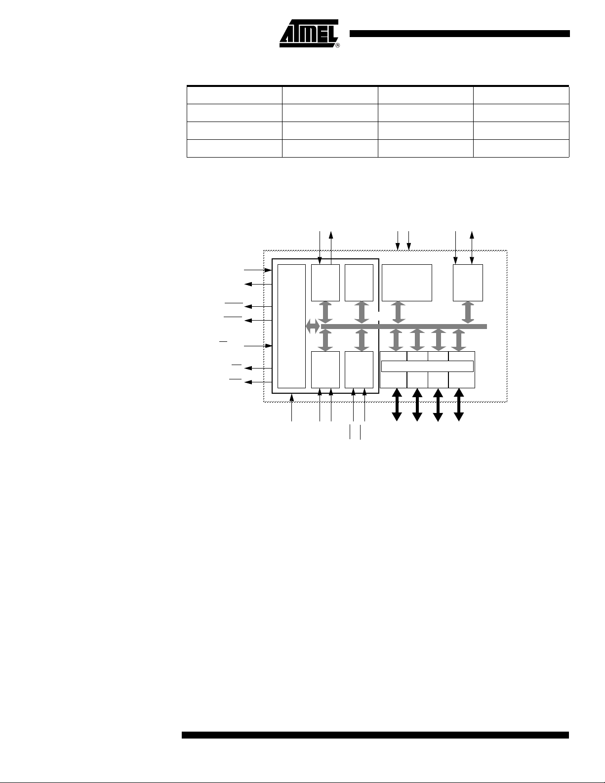
Block Diagram
Timer 0
INT
RAM
256x8
T0
T1
RxD
TxD
WR
RD
EA/VPP
PSEN
ALE/
XTAL2
XTAL1
EUART
CPU
Timer 1
INT1
Ctrl
INT0
(2)
(2)
C51
CORE
(2) (2) (2) (2)
Port 0P0Port 1
Port 2
Port 3
Parallel I/O Ports & Ext. Bus
P1
P2
P3
IB-bus
RESET
PROG
Vss
Vcc
(3)(3)
Timer2
T2EX
T2
(1) (1)
ROM
/EPROM
8Kx8
Table 1. Memory Size
ROM (bytes) EPROM (bytes) TOTAL RAM (bytes)
TS80C32X2 0 0 256
TS80C52X2 8k 0 256
TS87C52X2 0 8k 256
2
TS8xCx2X2
Notes: 1. Alternate function of Port 1
2. Alternate function of Port 3
4184I–8051–02/08
Page 3

TS8xCx2X2
SFR Mapping
The Special Function Registers (SFRs) of the TS80C52X2 fall into the following
categories:
• C51 core registers: ACC, B, DPH, DPL, PSW, SP, AUXR1
• I/O port registers: P0, P1, P2, P3
• Timer registers: T2CON, T2MOD, TCON, TH0, TH1, TH2, TMOD, TL0, TL1, TL2,
RCAP2L, RCAP2H
• Serial I/O port registers: SADDR, SADEN, SBUF, SCON
• Power and clock control registers: PCON
• Interrupt system registers: IE, IP, IPH
• Others: AUXR, CKCON
4184I–8051–02/08
3
Page 4
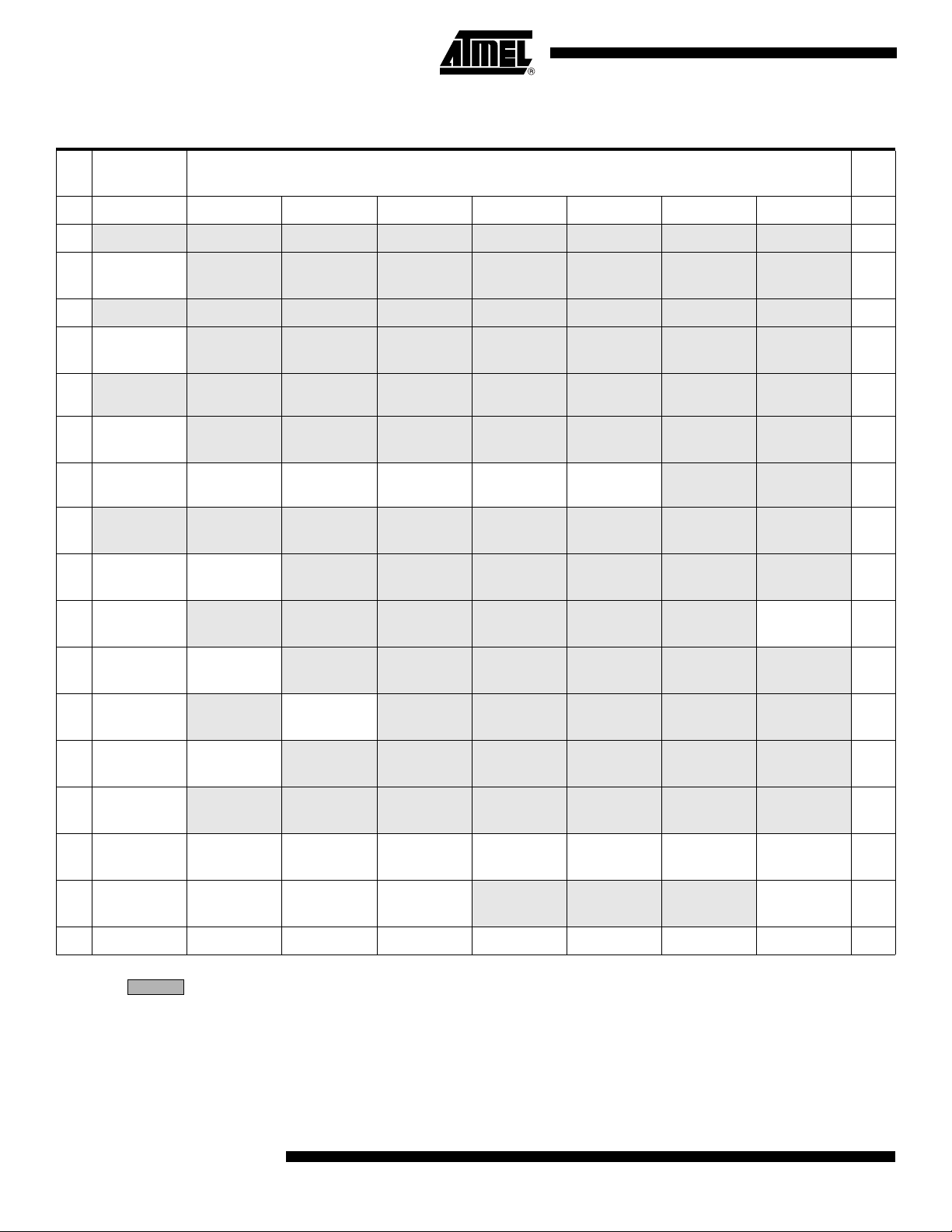
Table 2. All SFRs with their address and their reset value
Bit
Addressable Non Bit Addressable
0/8 1/9 2/A 3/B 4/C 5/D 6/E 7/F
F8h FFh
F0h
E8h EFh
E0h
D8
h
D0
h
C8
h
C0
h
B8h
B0h
A8h
A0h
B
0000 0000
ACC
0000 0000
PSW
0000 0000
T2CON
0000 0000
IP
XX00 0000
P3
1111 1111
IE
0X00 0000
P2
1111 1111
T2MOD
XXXX XX00
SADEN
0000 0000
SADDR
0000 0000
RCAP2L
0000 0000
AUXR1
XXXX XXX0
RCAP2H
0000 0000
TL2
0000 0000
TH2
0000 0000
IPH
XX00 0000
F7h
E7h
DFh
D7h
CFh
C7h
BFh
B7h
AFh
A7h
98h
90h
88h
80h
0000 0000
0000 0000
Reserved
4
SCON
P1
1111 1111
TCON
P0
1111 1111
0/8 1/9 2/A 3/B 4/C 5/D 6/E 7/F
SBUF
XXXX XXXX
TMOD
0000 0000
SP
0000 0111
TL0
0000 0000
DPL
0000 0000
TL1
0000 0000
DPH
0000 0000
TH0
0000 0000
TH1
0000 0000
AUXR
XXXXXXX0
TS8xCx2X2
CKCON
XXXX XXX0
PCON
00X1 0000
4184I–8051–02/08
9Fh
97h
8Fh
87h
Page 5
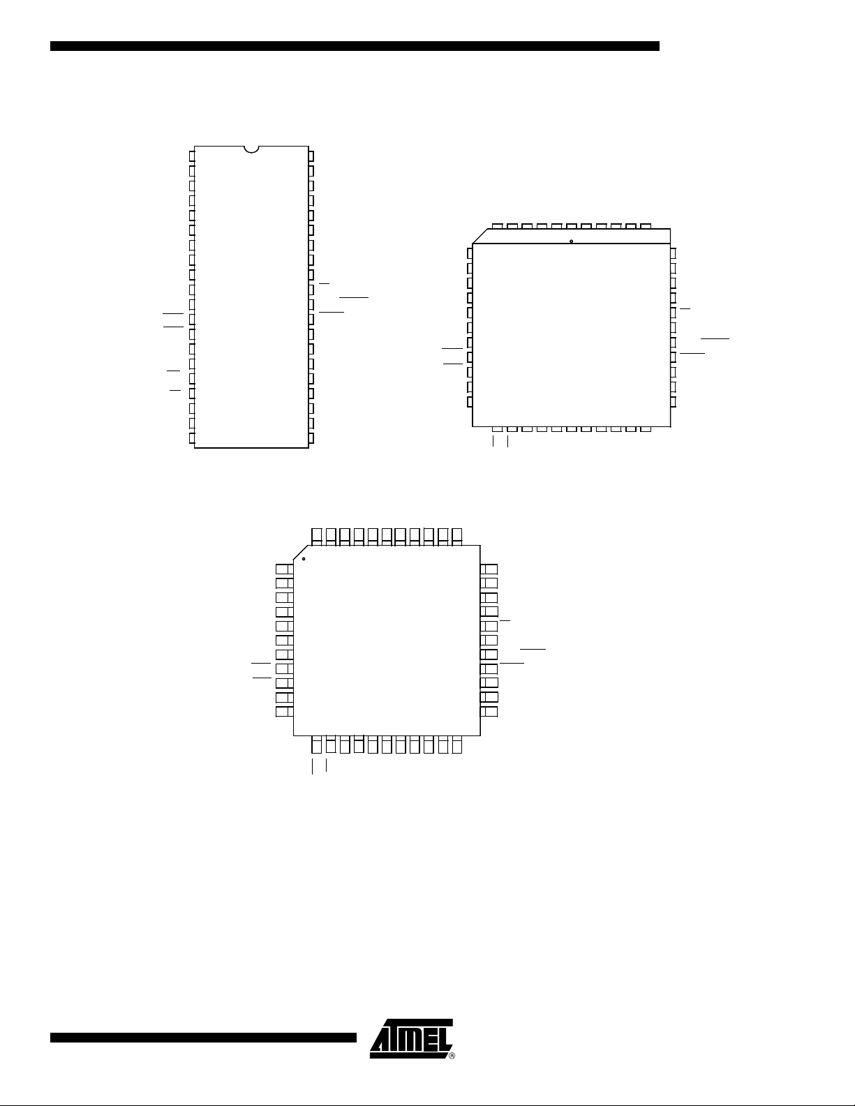
Pin Configuration
5 4 3 2 1 6
44 43 42 41 40
P1.4
P1.0/T2
P1.1/T2EX
P1.3
P1.2
VSS1/NIC*
VCC
P0.0/AD0
P0.2/AD2
P0.1/AD1
P0.4/AD4
P0.6/AD6
P0.5/AD5
P0.7/AD7
ALE/PROG
PSEN
EA/VPP
NIC*
P2.7/A15
P2.5/A13
P2.6/A14
P3.6/WR
P3.7/RD
XTAL2
XTAL1
VSS
P2.0/A8
P2.1/A9
P2.2/A10
P2.3/A11
P2.4/A12
43 42 41 40 3944
38 37 36 35 34
P1.4
P1.0/T2
P1.1/T2EX
P1.3
P1.2
VSS1/NIC*
VCC
P0.0/AD0
P0.2/AD2
P0.3/AD3
P0.1/AD1
P0.4/AD4
P0.6/AD6
P0.5/AD5
P0.7/AD7
ALE/PROG
PSEN
EA/VPP
NIC*
P2.7/A15
P2.5/A13
P2.6/A14
P1.5
P1.6
P1.7
RST
P3.0/RxD
NIC*
P3.1/TxD
P3.2/INT0
P3.3/INT1
P3.4/T0
P3.5/T1
P3.6/WR
P3.7/RD
XTAL2
XTAL1
VSS
P2.0/A8
P2.1/A9
P2.2/A10
P2.3/A11
P2.4/A12
P1.5
P1.6
P1.7
RST
P3.0/RxD
NIC*
P3.1/TxD
P3.2/INT0
P3.3/INT1
P3.4/T0
P3.5/T1
P0.3/AD3
NIC*
NIC*
*NIC: No Internal Connection
7
8
9
10
11
12
13
14
15
16
17
39
38
37
36
35
34
33
32
31
30
29
PLCC/CQPJ 44
33
32
31
30
29
28
27
26
25
24
23
PQFP44
1
2
3
4
5
6
7
8
9
10
11
18 19 20 21 22 23 24 25 26 27 28
12 13 14 15 16 17 18 19 20 21 22
VQFP44
P1.7
RST
P3.0/RxD
P3.1/TxD
P1.3
1
P1.5
P3.2/INT0
P3.3/INT1
P3.5/T1
P3.6/WR
P3.7/RD
XTAL2
XTAL1
VSS
P2.0 / A8
P2.1 / A9
P2.2 / A10
P2.3 / A11
P2.4 / A12
P0.4 / A4
P0.6 / A6
P0.5 / A5
P0.7 / A7
ALE/PROG
PSEN
EA/VPP
P2.7 / A15
P2.5 / A13
P2.6 / A14
P1.0 / T2
P1.1 / T2EX
VCC
P0.0 / A0
P0.1 / A1
P0.2 / A2
P0.3 / A3
PDIL/
2
3
4
5
6
7
8
9
10
11
12
13
14
15
16
17
18
19
20
40
39
38
37
36
35
34
33
32
31
30
29
28
27
26
25
24
23
22
21
CDIL40
P1.6
P1.4
P1.2
P3.4/T0
TS8xCx2X2
4184I–8051–02/08
5
Page 6
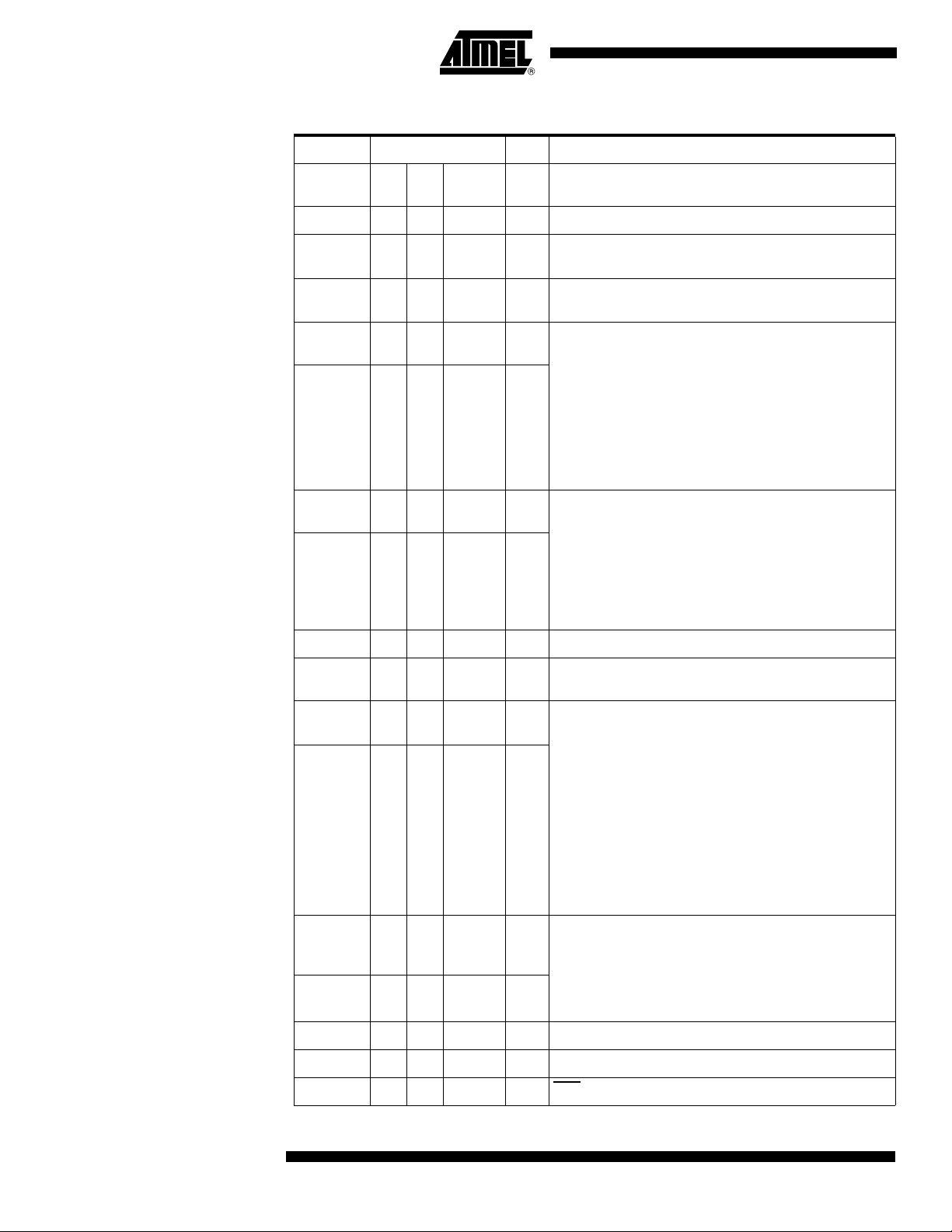
Mnemonic Pin Number Type Name and Function
VQFP
DIL LCC
1.4
V
SS
Vss1 1 39 I
V
CC
P0.0-P0.7
P1.0-P1.7 1-8 2-9 40-44
20 22 16 I Ground: 0V reference
40 44 38 I
39-3243-
1 2 40 I/O T2 (P1.0): Timer/Counter 2 external count input/Clockout
2 3 41 I
36
37-30 I/O
1-3
Optional Ground: Contact the Sales Office for ground
connection.
Power Supply: This is the power supply voltage for normal,
idle and power-down operation
Port 0: Port 0 is an open-drain, bidirectional I/O port. Port 0
pins that have 1s written to them float and can be used as
high impedance inputs.Port 0 pins must be polarized to Vcc
or Vss in order to prevent any parasitic current consumption.
Port 0 is also the multiplexed low-order address and data bus
during access to external program and data memory. In this
application, it uses strong internal pull-up when emitting 1s.
Port 0 also inputs the code bytes during EPROM
programming. External pull-ups are required during program
verification during which P0 outputs the code bytes.
I/O Port 1: Port 1 is an 8-bit bidirectional I/O port with internal
pull-ups. Port 1 pins that have 1s written to them are pulled
high by the internal pull-ups and can be used as inputs. As
inputs, Port 1 pins that are externally pulled low will source
current because of the internal pull-ups. Port 1 also receives
the low-order address byte during memory programming and
verification.
Alternate functions for Port 1 include:
T2EX (P1.1): Timer/Counter 2 Reload/Capture/Direction
Control
P2.0-P2.7
P3.0-P3.7
6
TS8xCx2X2
21-2824-
10-1711,
10 11 5 I RXD (P3.0): Serial input port
11 13 7 O TXD (P3.1): Serial output port
12 14 8 I INT0 (P3.2): External interrupt 0
31
13-
19
18-25 I/O
5,
7-13
Port 2: Port 2 is an 8-bit bidirectional I/O port with internal
pull-ups. Port 2 pins that have 1s written to them are pulled
high by the internal pull-ups and can be used as inputs. As
inputs, Port 2 pins that are externally pulled low will source
current because of the internal pull-ups. Port 2 emits the highorder address byte during fetches from external program
memory and during accesses to external data memory that
use 16-bit addresses (MOVX atDPTR).In this application, it
uses strong internal pull-ups emitting 1s. During accesses to
external data memory that use 8-bit addresses (MOVX atRi),
port 2 emits the contents of the P2 SFR. Some Port 2 pins
receive the high order address bits during EPROM
programming and verification: P2.0 to P2.4
Port 3: Port 3 is an 8-bit bidirectional I/O port with internal
I/O
pull-ups. Port 3 pins that have 1s written to them are pulled
high by the internal pull-ups and can be used as inputs. As
inputs, Port 3 pins that are externally pulled low will source
current because of the internal pull-ups. Port 3 also serves
the special features of the 80C51 family, as listed below.
4184I–8051–02/08
Page 7
Mnemonic Pin Number Type Name and Function
VQFP
DIL LCC
13 15 9 I INT1 (P3.3): External interrupt 1
14 16 10 I T0 (P3.4): Timer 0 external input
15 17 11 I T1 (P3.5): Timer 1 external input
16 18 12 O WR (P3.6): External data memory write strobe
17 19 13 O RD (P3.7): External data memory read strobe
1.4
TS8xCx2X2
Reset 9 10 4 I Reset: A high on this pin for two machine cycles while the
ALE/PROG 30 33 27 O (I) Address Latch Enable/Program Pulse: Output pulse for
PSEN 29 32 26 O Program Store ENable: The read strobe to external program
EA/V
PP
31 35 29 I External Access Enable/Programming Supply Voltage:
oscillator is running, resets the device. An internal diffused
resistor to V
external capacitor to V
latching the low byte of the address during an access to
external memory. In normal operation, ALE is emitted at a
constant rate of 1/6 (1/3 in X2 mode) the oscillator frequency,
and can be used for external timing or clocking. Note that one
ALE pulse is skipped during each access to external data
memory. This pin is also the program pulse input (PROG)
during EPROM programming. ALE can be disabled by setting
SFR’s AUXR.0 bit. With this bit set, ALE will be inactive
during internal fetches.
memory. When executing code from the external program
memory, PSEN is activated twice each machine cycle, except
that two PSEN activations are skipped during each access to
external data memory. PSEN is not activated during fetches
from internal program memory.
EA must be externally held low to enable the device to fetch
code from external program memory locations 0000H and
3FFFH (RB) or 7FFFH (RC), or FFFFH (RD). If EA is held
high, the device executes from internal program memory
unless the program counter contains an address greater than
3FFFH (RB) or 7FFFH (RC) EA must be held low for
ROMless devices. This pin also receives the 12.75V
programming supply voltage (VPP) during EPROM
programming. If security level 1 is programmed, EA will be
internally latched on Reset.
permits a power-on reset using only an
SS
CC.
4184I–8051–02/08
XTAL1 19 21 15 I
XTAL2 18 20 14 O Crystal 2: Output from the inverting oscillator amplifier
Crystal 1: Input to the inverting oscillator amplifier and input
to the internal clock generator circuits.
7
Page 8
XTAL1
2
CKCON reg
X2
state machine: 6 clock cycles.
CPU control
F
OSC
F
XTAL
0
1
XTAL1:2
TS80C52X2 Enhanced Features
X2 Feature
In comparison to the original 80C52, the TS80C52X2 implements some new features,
which are
:
• The X2 option
• The Dual Data Pointer
• The 4 level interrupt priority system
• The power-off flag
• The ONCE mode
• The ALE disabling
• Some enhanced features are also located in the UART and the Timer 2
The TS80C52X2 core needs only 6 clock periods per machine cycle. This feature called
”X2” provides the following advantages:
• Divide frequency crystals by 2 (cheaper crystals) while keeping same CPU power
• Save power consumption while keeping same CPU power (oscillator power saving)
• Save power consumption by dividing dynamically operating frequency by 2 in
operating and idle modes
• Increase CPU power by 2 while keeping same crystal frequency
In order to keep the original C51 compatibility, a divider by 2 is inserted between the
XTAL1 signal and the main clock input of the core (phase generator). This divider may
be disabled by software.
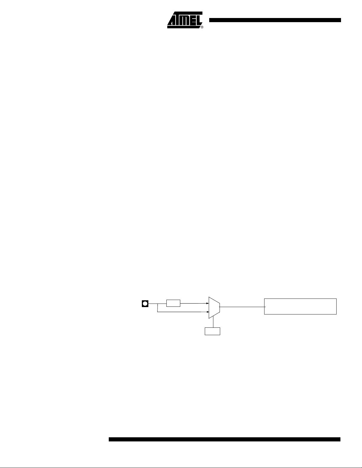
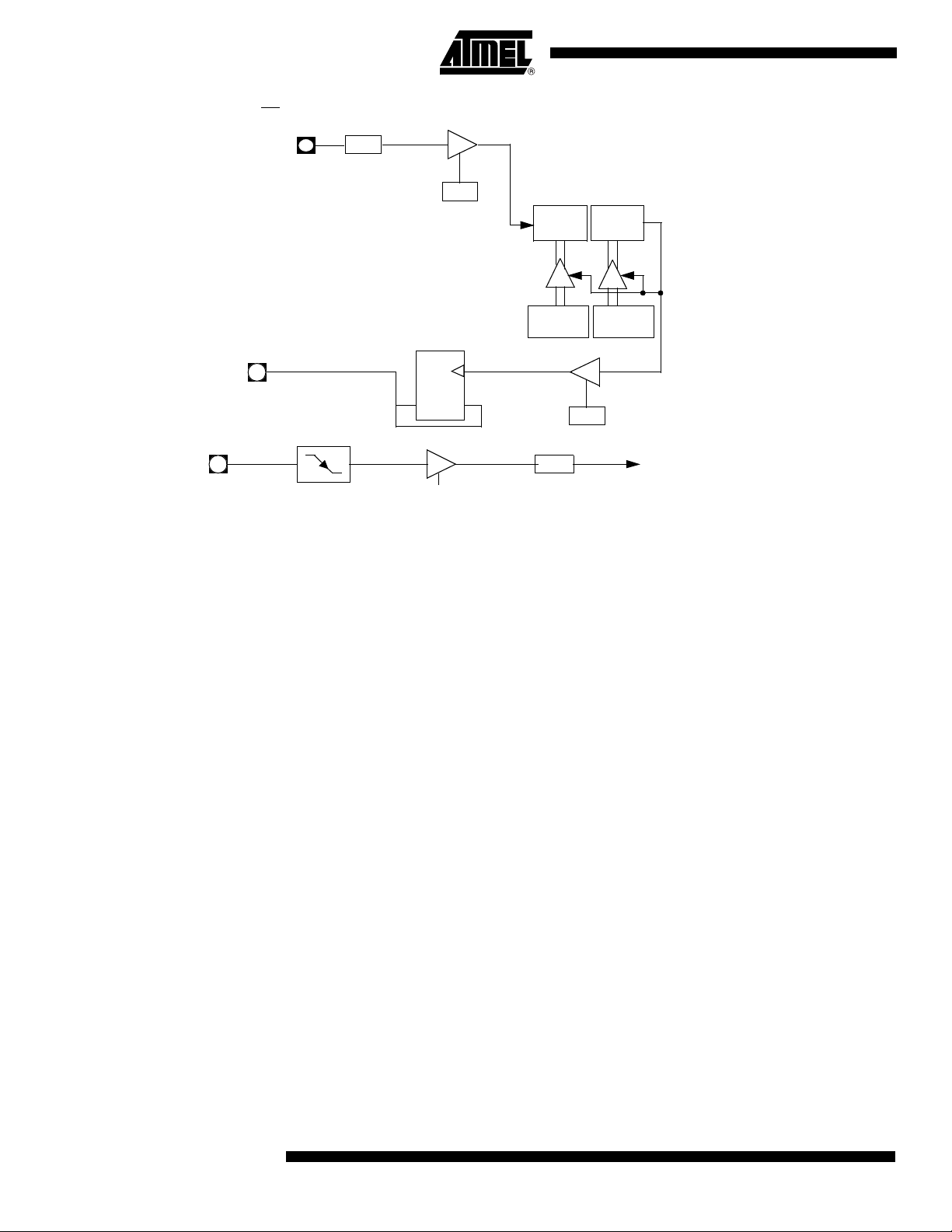
Description The clock for the whole circuit and peripheral is first divided by two before being used by
the CPU core and peripherals. This allows any cyclic ratio to be accepted on XTAL1
input. In X2 mode, as this divider is bypassed, the signals on XTAL1 must have a cyclic
ratio between 40 to 60%. Figure 1. shows the clock generation block diagram. X2 bit is
validated on XTAL1÷2 rising edge to avoid glitches when switching from X2 to STD
mode. Figure 2 shows the mode switching waveforms.
Figure 1. Clock Generation Diagram
8
TS8xCx2X2
4184I–8051–02/08
Page 9
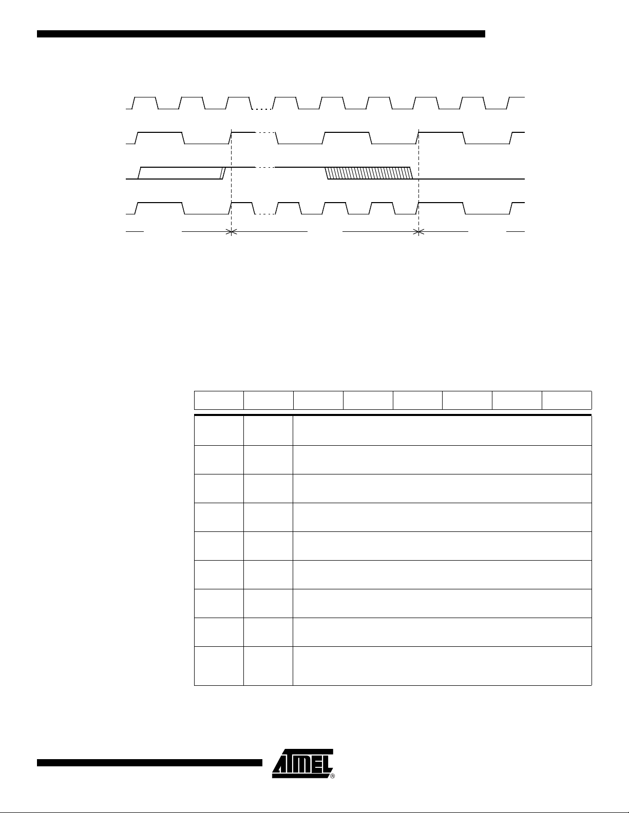
Figure 2. Mode Switching Waveforms
XTAL1:2
XTAL1
CPU clock
X2 bit
X2 ModeSTD Mode STD Mode
The X2 bit in the CKCON register (See Table 3.) allows to switch from 12 clock cycles
per instruction to 6 clock cycles and vice versa. At reset, the standard speed is activated
(STD mode). Setting this bit activates the X2 feature (X2 mode).
Note: In order to prevent any incorrect operation while operating in X2 mode, user must be
Table 3. CKCON Register
CKCON - Clock Control Register (8Fh)
TS8xCx2X2
aware that all peripherals using clock frequency as time reference (UART, timers) will
have their time reference divided by two. For example a free running timer generating an
interrupt every 20 ms will then generate an interrupt every 10 ms. UART with 4800 baud
rate will have 9600 baud rate.
7 6 5 4 3 2 1 0
- - - - - - - X2
Bit
Number
7 -
6 -
5 -
4 -
3 -
2 -
1 -
0 X2
Bit
Mnemonic Description
Reserved
The value read from this bit is indeterminate. Do not set this bit.
Reserved
The value read from this bit is indeterminate. Do not set this bit.
Reserved
The value read from this bit is indeterminate. Do not set this bit.
Reserved
The value read from this bit is indeterminate. Do not set this bit.
Reserved
The value read from this bit is indeterminate. Do not set this bit.
Reserved
The value read from this bit is indeterminate. Do not set this bit.
Reserved
The value read from this bit is indeterminate. Do not set this bit.
CPU and peripheral clock bit
Clear to select 12 clock periods per machine cycle (STD mode, F
Set to select 6 clock periods per machine cycle (X2 mode, F
OSC=FXTAL
OSC=FXTAL
/
2).
).
Reset Value = XXXX XXX0b
Not bit addressable
For further details on the X2 feature, please refer to ANM072 available on the web
(http://www.atmel.com)
4184I–8051–02/08
9
Page 10
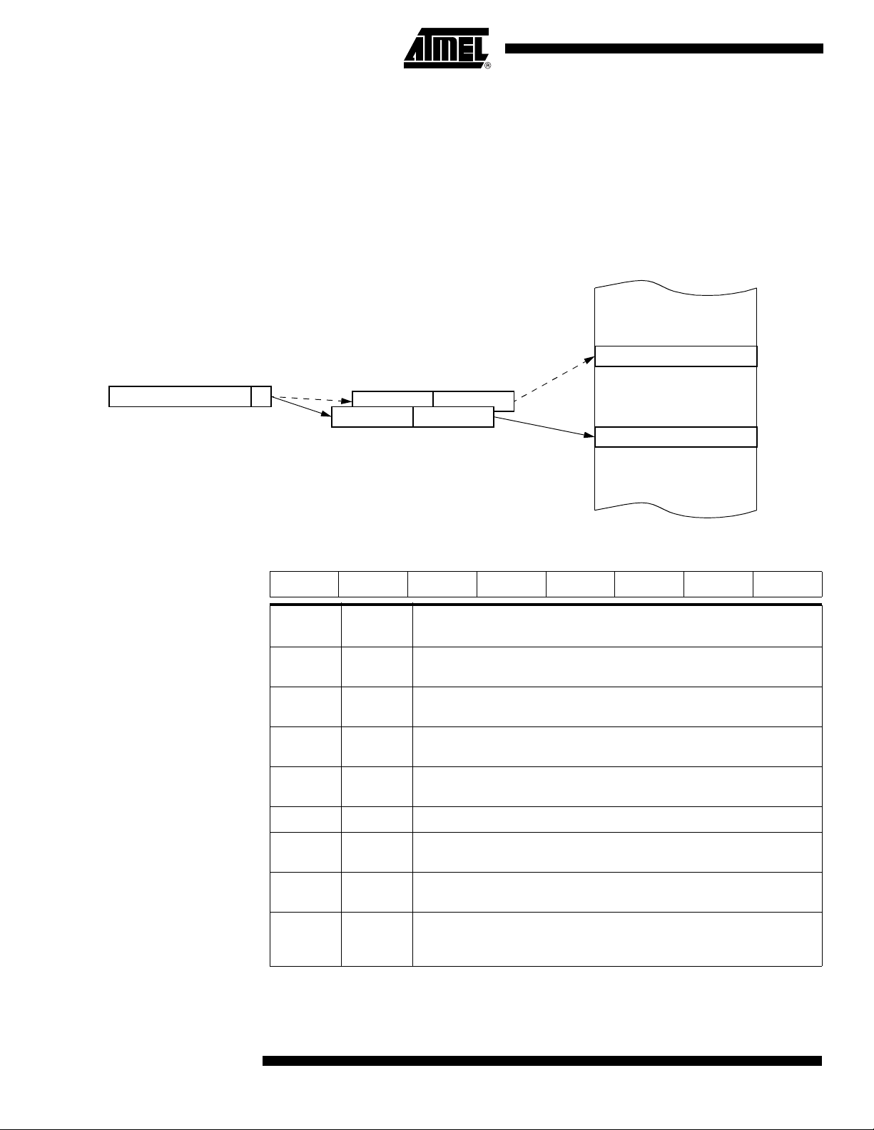
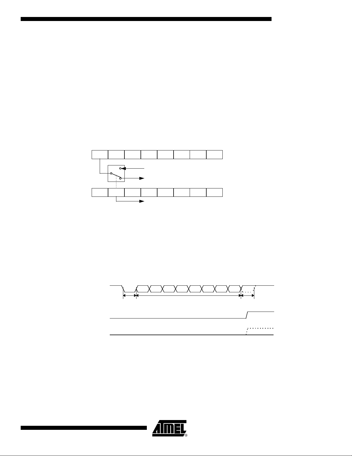
External Data Memory
AUXR1(A2H)
DPS
DPH(83H) DPL(82H)
07
DPTR0
DPTR1
Dual Data Pointer Register (Ddptr)
Figure 3. Use of Dual Pointer
The additional data pointer can be used to speed up code execution and reduce code
size in a number of ways.
The dual DPTR structure is a way by which the chip will specify the address of an external data memory location. There are two 16-bit DPTR registers that address the external
memory, and a single bit called
DPS = AUXR1/bit0 (See Table 5.) that allows the program code to switch between them
(Refer to Figure 3).
Table 4. AUXR1: Auxiliary Register 1
7 6 5 4 3 2 1 0
- - - - GF3 0 - DPS
Bit
Number
7 -
6 -
5 -
4 -
3 GF3 This bit is a general purpose user flag
2 0
1 -
0 DPS
Bit
Mnemonic Description
Reserved
The value read from this bit is indeterminate. Do not set this bit.
Reserved
The value read from this bit is indeterminate. Do not set this bit.
Reserved
The value read from this bit is indeterminate. Do not set this bit.
Reserved
The value read from this bit is indeterminate. Do not set this bit.
Reserved
Always stuck at 0
Reserved
The value read from this bit is indeterminate. Do not set this bit.
Data Pointer Selection
Clear to select DPTR0.
Set to select DPTR1.
10
TS8xCx2X2
Reset Value = XXXX XXX0
Not bit addressable
4184I–8051–02/08
Page 11

TS8xCx2X2
Application
Software can take advantage of the additional data pointers to both increase speed and
reduce code size, for example, block operations (copy, compare, search ...) are well
served by using one data pointer as a ’source’ pointer and the other one as a "destination" pointer.
ASSEMBLY LANGUAGE
; Block move using dual data pointers
; Destroys DPTR0, DPTR1, A and PSW
; note: DPS exits opposite of entry state
; unless an extra INC AUXR1 is added
;
00A2 AUXR1 EQU 0A2H
;
0000 909000MOV DPTR,#SOURCE ; address of SOURCE
0003 05A2 INC AUXR1 ; switch data pointers
0005 90A000 MOV DPTR,#DEST ; address of DEST
0008 LOOP:
0008 05A2 INC AUXR1 ; switch data pointers
000A E0 MOVX A,atDPTR ; get a byte from SOURCE
000B A3 INC DPTR ; increment SOURCE address
000C 05A2 INC AUXR1 ; switch data pointers
000E F0 MOVX atDPTR,A ; write the byte to DEST
000F A3 INC DPTR ; increment DEST address
0010 70F6JNZ LOOP ; check for 0 terminator
0012 05A2 INC AUXR1 ; (optional) restore DPS
INC is a short (2 bytes) and fast (12 clocks) way to manipulate the DPS bit in the AUXR1
SFR. However, note that the INC instruction does not directly force the DPS bit to a particular state, but simply toggles it. In simple routines, such as the block move example,
only the fact that DPS is toggled in the proper sequence matters, not its actual value. In
other words, the block move routine works the same whether DPS is '0' or '1' on entry.
Observe that without the last instruction (INC AUXR1), the routine will exit with DPS in
the opposite state.
4184I–8051–02/08
11
Page 12

Timer 2
Auto-reload Mode The Auto-reload mode configures timer 2 as a 16-bit timer or event counter with auto-
The timer 2 in the
It is a 16-bit timer/counter: the count is maintained by two eight-bit timer registers, TH2
and TL2, connected in cascade. It is controlled by T2CON register (See Table 5) and
T2MOD register (See Table 6). Timer 2 operation is similar to Timer 0 and Timer 1. C/T2
selects F
clock input. Setting TR2 allows TL2 to be incremented by the selected input.
Timer 2 has 3 operating modes: capture, autoreload and Baud Rate Generator. These
modes are selected by the combination of RCLK, TCLK and CP/RL2 (T2CON), as
described in the Atmel 8-bit Microcontroller Hardware description.
Refer to the Atmel 8-bit Microcontroller Hardware description for the description of Capture and Baud Rate Generator Modes.
In
TS80C52X2
• Auto-reload mode with up or down counter
• Programmable clock-output
matic reload. If DCEN bit in T2MOD is cleared, timer 2 behaves as in 80C52 (refer to the
Atmel 8-bit Microcontroller Hardware description). If DCEN bit is set, timer 2 acts as an
Up/down timer/counter as shown in Figure 4. In this mode the T2EX pin controls the
direction of count.
When T2EX is high, timer 2 counts up. Timer overflow occurs at FFFFh which sets the
TF2 flag and generates an interrupt request. The overflow also causes the 16-bit value
in RCAP2H and RCAP2L registers to be loaded into the timer registers TH2 and TL2.
OSC
TS80C52X2
/12 (timer operation) or external pin T2 (counter operation) as the timer
Timer 2 includes the following enhancements:
is compatible with the timer 2 in the 80C52.
When T2EX is low, timer 2 counts down. Timer underflow occurs when the count in the
timer registers TH2 and TL2 equals the value stored in RCAP2H and RCAP2L registers.
The underflow sets TF2 flag and reloads FFFFh into the timer registers.
The EXF2 bit toggles when timer 2 overflows or underflows according to the the direction of the count. EXF2 does not generate any interrupt. This bit can be used to provide
17-bit resolution.
12
TS8xCx2X2
4184I–8051–02/08
Page 13
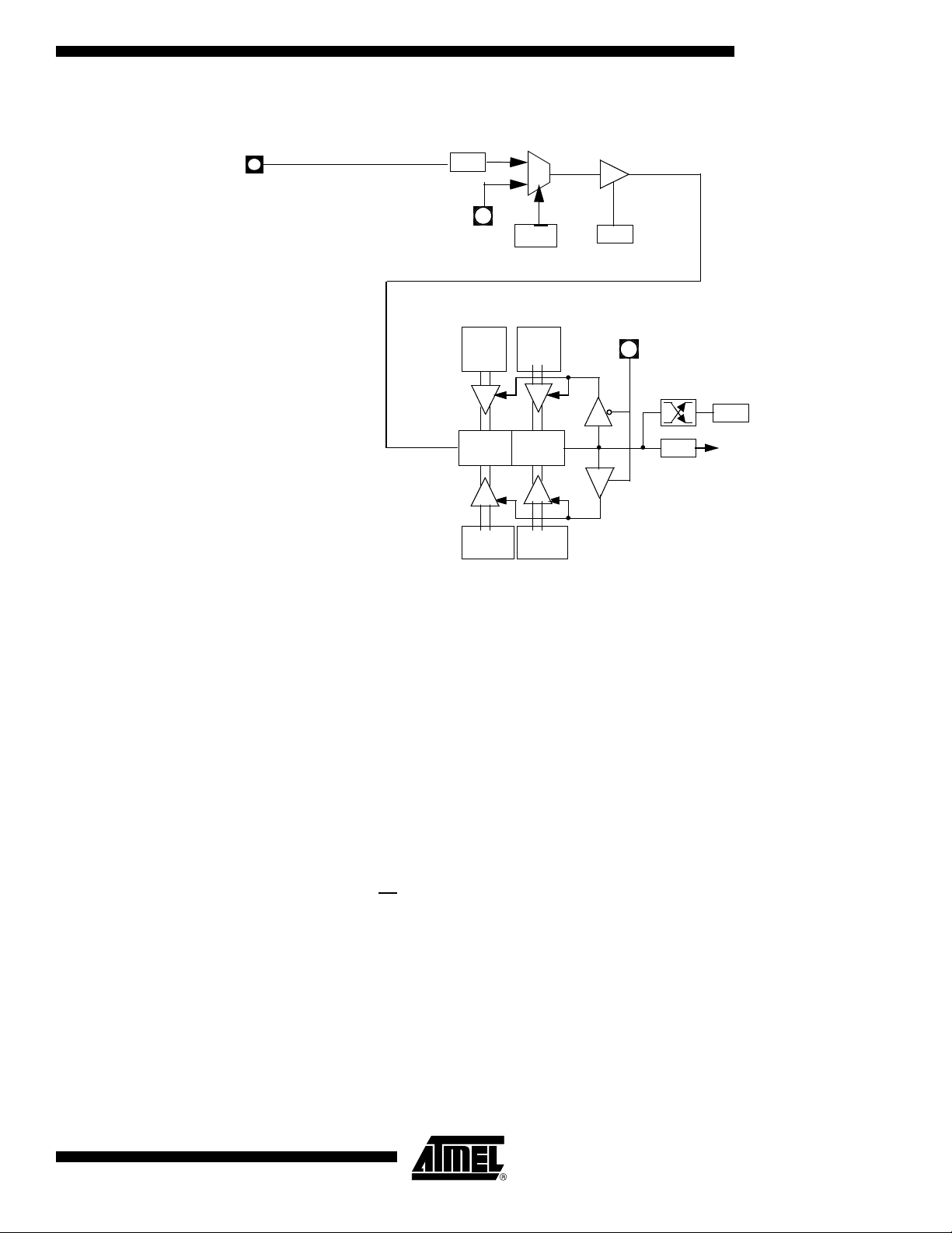
Figure 4. Auto-reload Mode Up/Down Counter (DCEN = 1)
(DOWN COUNTING RELOAD
C/T2
TF2
TR2
T2
EXF2
TH2
(8-bit)
TL2
(8-bit)
RCAP2H
(8-bit)
RCAP2L
(8-bit)
FFh
(8-bit)
FFh
(8-bit)
TOGGL
(UP COUNTING RELOAD VALUE)
TIMER 2
INTERRUPT
XTAL1
:12
F
OSC
F
XTAL
0
1
T2CONreg
T2CONreg
T2CONreg
T2CONreg
T2EX:
if DCEN=1, 1=UP
if DCEN=1, 0=DOWN
if DCEN = 0, up counting
(:6 in X2 mode)
Clo c k O utFreque n c y–
F
osc
4 65536 RCAP2H– RCAP2L⁄( )×
-----------------------------------------------------------------------------------------
=
TS8xCx2X2
Programmable Clock-output In the clock-out mode, timer 2 operates as a 50%-duty-cycle, programmable clock gen-
erator (See Figure 5) . The input clock increments TL2 at frequency F
/2. The timer
OSC
repeatedly counts to overflow from a loaded value. At overflow, the contents of RCAP2H
and RCAP2L registers are loaded into TH2 and TL2. In this mode, timer 2 overflows do
not generate interrupts. The formula gives the clock-out frequency as a function of the
system oscillator frequency and the value in the RCAP2H and RCAP2L registers :
For a 16 MHz system clock, timer 2 has a programmable frequency range of 61 Hz
(F
/2
OSC
Timer 2 is programmed for the clock-out mode as follows:
• Set T2OE bit in T2MOD register.
• Clear C/T2 bit in T2CON register.
16)
to 4 MHz (F
/4). The generated clock signal is brought out to T2 pin (P1.0).
OSC
• Determine the 16-bit reload value from the formula and enter it in RCAP2H/RCAP2L
registers.
• Enter a 16-bit initial value in timer registers TH2/TL2. It can be the same as the
reload value or a different one depending on the application.
• To start the timer, set TR2 run control bit in T2CON register.
It is possible to use timer 2 as a baud rate generator and a clock generator simultaneously. For this configuration, the baud rates and clock frequencies are not
independent since both functions use the values in the RCAP2H and RCAP2L registers.
4184I–8051–02/08
13
Page 14
:2
EXF2
TR2
OVERFLOW
T2EX
TH2
(8-bit)
TL2
(8-bit)
TIMER 2
RCAP2H
(8-bit)
RCAP2L
(8-bit)
T2OE
T2
XTAL1
T2CON reg
T2CON reg
T2CON reg
T2MOD reg
INTERRUPT
Q D
Toggle
EXEN2
(:1 in X2 mode)
Figure 5. Clock-Out Mode C/T2 = 0
14
TS8xCx2X2
4184I–8051–02/08
Page 15

TS8xCx2X2
Table 5. T2CON Register
T2CON - Timer 2 Control Register (C8h)
7 6 5 4 3 2 1 0
TF2 EXF2 RCLK TCLK EXEN2 TR2 C/T2# CP/RL2#
Bit
Number
Mnemonic Description
7 TF2
6 EXF2
5 RCLK
4 TCLK
3 EXEN2
2 TR2
1 C/T2#
0 CP/RL2#
Bit
Timer 2 overflow Flag
Must be cleared by software.
Set by hardware on timer 2 overflow, if RCLK = 0 and TCLK = 0.
Timer 2 External Flag
Set when a capture or a reload is caused by a negative transition on T2EX pin if
EXEN2=1.
When set, causes the CPU to vector to timer 2 interrupt routine when timer 2
interrupt is enabled.
Must be cleared by software. EXF2 doesn’t cause an interrupt in Up/down counter
mode (DCEN = 1)
Receive Clock bit
Clear to use timer 1 overflow as receive clock for serial port in mode 1 or 3.
Set to use timer 2 overflow as receive clock for serial port in mode 1 or 3.
Transmit Clock bit
Clear to use timer 1 overflow as transmit clock for serial port in mode 1 or 3.
Set to use timer 2 overflow as transmit clock for serial port in mode 1 or 3.
Timer 2 External Enable bit
Clear to ignore events on T2EX pin for timer 2 operation.
Set to cause a capture or reload when a negative transition on T2EX pin is
detected, if timer 2 is not used to clock the serial port.
Timer 2 Run control bit
Clear to turn off timer 2.
Set to turn on timer 2.
Timer/Counter 2 select bit
Clear for timer operation (input from internal clock system: F
Set for counter operation (input from T2 input pin, falling edge trigger). Must be 0
for clock out mode.
Timer 2 Capture/Reload bit
If RCLK=1 or TCLK=1, CP/RL2# is ignored and timer is forced to Auto-reload on
timer 2 overflow.
Clear to Auto-reload on timer 2 overflows or negative transitions on T2EX pin if
EXEN2=1.
Set to capture on negative transitions on T2EX pin if EXEN2=1.
OSC
).
4184I–8051–02/08
Reset Value = 0000 0000b
Bit addressable
15
Page 16

Table 6. T2MOD Register
T2MOD - Timer 2 Mode Control Register (C9h)
7 6 5 4 3 2 1 0
- - - - - - T2OE DCEN
Bit
Number
7 -
6 -
5 -
4 -
3 -
2 -
1 T2OE
0 DCEN
Bit
Mnemonic Description
Reserved
The value read from this bit is indeterminate. Do not set this bit.
Reserved
The value read from this bit is indeterminate. Do not set this bit.
Reserved
The value read from this bit is indeterminate. Do not set this bit.
Reserved
The value read from this bit is indeterminate. Do not set this bit.
Reserved
The value read from this bit is indeterminate. Do not set this bit.
Reserved
The value read from this bit is indeterminate. Do not set this bit.
Timer 2 Output Enable bit
Clear to program P1.0/T2 as clock input or I/O port.
Set to program P1.0/T2 as clock output.
Down Counter Enable bit
Clear to disable timer 2 as up/down counter.
Set to enable timer 2 as up/down counter.
Reset Value = XXXX XX00b
Not bit addressable
16
TS8xCx2X2
4184I–8051–02/08
Page 17
TS8xCx2X2
RITIRB8TB8RENSM2SM1SM0/FE
IDLPDGF0GF1POF-SMOD0SMOD1
To UART framing error control
SM0 to UART mode control (SMOD = 0)TS80C52X2
Set FE bit if stop bit is 0 (framing error) (SMOD0 = 1)
SCON (98h)
PCON (87h)
Data byte
RI
SMOD0=X
Stop
bit
Start
bit
RXD
D7D6D5D4D3D2D1D0
FE
SMOD0=1
TS80C52X2 Serial I/O Port
The serial I/O port in the TS80C52X2 is compatible with the serial I/O port in the 80C52.
It provides both synchronous and asynchronous communication modes. It operates as
an Universal Asynchronous Receiver and Transmitter (UART) in three full-duplex
modes (Modes 1, 2 and 3). Asynchronous transmission and reception can occur simultaneously and at different baud rates
Serial I/O port includes the following enhancements:
• Framing error detection
• Automatic address recognition
Framing Error Detection Framing bit error detection is provided for the three asynchronous modes (modes 1, 2
and 3). To enable the framing bit error detection feature, set SMOD0 bit in PCON register (See Figure 6).
Figure 6. Framing Error Block Diagram
Figure 7. UART Timings in Mode 1
When this feature is enabled, the receiver checks each incoming data frame for a valid
stop bit. An invalid stop bit may result from noise on the serial lines or from simultaneous
transmission by two CPUs. If a valid stop bit is not found, the Framing Error bit (FE) in
SCON register (See Table 9.) bit is set.
Software may examine FE bit after each reception to check for data errors. Once set,
only software or a reset can clear FE bit. Subsequently received frames with valid stop
bits cannot clear FE bit. When FE feature is enabled, RI rises on stop bit instead of the
last data bit (See Figure 7. and Figure 8.).
4184I–8051–02/08
17
Page 18

RI
SMOD0=0
Data byte Ninth
bit
Stop
bit
Start
bit
RXD
D8D7D6D5D4D3D2D1D0
RI
SMOD0=1
FE
SMOD0=1
Figure 8. UART Timings in Modes 2 and 3
Automatic Address Recognition
The automatic address recognition feature is enabled when the multiprocessor communication feature is enabled (SM2 bit in SCON register is set).
Implemented in hardware, automatic address recognition enhances the multiprocessor
communication feature by allowing the serial port to examine the address of each
incoming command frame. Only when the serial port recognizes its own address, the
receiver sets RI bit in SCON register to generate an interrupt. This ensures that the CPU
is not interrupted by command frames addressed to other devices.
If desired, you may enable the automatic address recognition feature in mode 1. In this
configuration, the stop bit takes the place of the ninth data bit. Bit RI is set only when the
received command frame address matches the device’s address and is terminated by a
valid stop bit.
To support automatic address recognition, a device is identified by a given address and
a broadcast address.
Note: The multiprocessor communication and automatic address recognition features cannot
be enabled in mode 0 (i.e. setting SM2 bit in SCON register in mode 0 has no effect).
Given Address Each device has an individual address that is specified in SADDR register; the SADEN
register is a mask byte that contains don’t-care bits (defined by zeros) to form the
device’s given address. The don’t-care bits provide the flexibility to address one or more
slaves at a time. The following example illustrates how a given address is formed.
To address a device by its individual address, the SADEN mask byte must be 1111
1111b.
For example:
SADDR0101 0110b
SADEN1111 1100b
Given0101 01XXb
18
TS8xCx2X2
The following is an example of how to use given addresses to address different slaves:
Slave A:SADDR1111 0001b
SADEN1111 1010b
Given1111 0X0Xb
Slave B:SADDR1111 0011b
SADEN1111 1001b
Given1111 0XX1b
Slave C:SADDR1111 0010b
SADEN1111 1101b
Given1111 00X1b
The SADEN byte is selected so that each slave may be addressed separately.
For slave A, bit 0 (the LSB) is a don’t-care bit; for slaves B and C, bit 0 is a 1. To communicate with slave A only, the master must send an address where bit 0 is clear (e.g.
4184I–8051–02/08
Page 19

TS8xCx2X2
1111 0000b).
For slave A, bit 1 is a 1; for slaves B and C, bit 1 is a don’t care bit. To communicate with
slaves B and C, but not slave A, the master must send an address with bits 0 and 1 both
set (e.g. 1111 0011b).
To communicate with slaves A, B and C, the master must send an address with bit 0
set, bit 1 clear, and bit 2 clear (e.g. 1111 0001b).
Broadcast Address A broadcast address is formed from the logical OR of the SADDR and SADEN registers
with zeros defined as don’t-care bits, e.g.:
SADDR 0101 0110b
SADEN 1111 1100b
Broadcast =SADDR OR SADEN1111 111Xb
The use of don’t-care bits provides flexibility in defining the broadcast address, however
in most applications, a broadcast address is FFh. The following is an example of using
broadcast addresses:
Slave A:SADDR1111 0001b
SADEN1111 1010b
Broadcast1111 1X11b,
Slave B:SADDR1111 0011b
SADEN1111 1001b
Broadcast1111 1X11B,
Slave C:SADDR=1111 0010b
SADEN1111 1101b
Broadcast1111 1111b
For slaves A and B, bit 2 is a don’t care bit; for slave C, bit 2 is set. To communicate with
all of the slaves, the master must send an address FFh. To communicate with slaves A
and B, but not slave C, the master can send and address FBh.
Reset Addresses On reset, the SADDR and SADEN registers are initialized to 00h, i.e. the given and
broadcast addresses are XXXX XXXXb (all don’t-care bits). This ensures that the serial
port will reply to any address, and so, that it is backwards compatible with the 80C51
microcontrollers that do not support automatic address recognition.
Table 7. SADEN Register
SADEN - Slave Address Mask Register (B9h)
7 6 5 4 3 2 1 0
Reset Value = 0000 0000b
Not bit addressable
Table 8. SADDR Register
SADDR - Slave Address Register (A9h)
7 6 5 4 3 2 1 0
4184I–8051–02/08
Reset Value = 0000 0000b
Not bit addressable
19
Page 20

Table 9. SCON Register
SCON - Serial Control Register (98h)
7 6 5 4 3 2 1 0
FE/SM0 SM1 SM2 REN TB8 RB8 TI RI
Bit
Number
7 FE
6 SM1
5 SM2
4 REN
3 TB8
Bit
Mnemonic Description
Framing Error bit (SMOD0=1)
Clear to reset the error state, not cleared by a valid stop bit.
Set by hardware when an invalid stop bit is detected.
SMOD0 must be set to enable access to the FE bit
Serial port Mode bit 0
SM0
Refer to SM1 for serial port mode selection.
SMOD0 must be cleared to enable access to the SM0 bit
Serial port Mode bit 1
SM0 SM1 Mode Description Baud Rate
0 0 0 Shift Register F
0 1 1 8-bit UART Variable
1 0 2 9-bit UART F
1 1 3 9-bit UART Variable
Serial port Mode 2 bit / Multiprocessor Communication Enable bit
Clear to disable multiprocessor communication feature.
Set to enable multiprocessor communication feature in mode 2 and 3, and
eventually mode 1. This bit should be cleared in mode 0.
Reception Enable bit
Clear to disable serial reception.
Set to enable serial reception.
Transmitter Bit 8 / Ninth bit to transmit in modes 2 and 3.
Clear to transmit a logic 0 in the 9th bit.
Set to transmit a logic 1 in the 9th bit.
/12 (/6 in X2 mode)
XTAL
/64 or F
XTAL
XTAL
/32 (/32, /16 in X2 mode)
Receiver Bit 8 / Ninth bit received in modes 2 and 3
2 RB8
1 TI
0 RI
Cleared by hardware if 9th bit received is a logic 0.
Set by hardware if 9th bit received is a logic 1.
In mode 1, if SM2 = 0, RB8 is the received stop bit. In mode 0 RB8 is not used.
Transmit Interrupt flag
Clear to acknowledge interrupt.
Set by hardware at the end of the 8th bit time in mode 0 or at the beginning of the
stop bit in the other modes.
Receive Interrupt flag
Clear to acknowledge interrupt.
Set by hardware at the end of the 8th bit time in mode 0, see Figure 7. and Figure
8. in the other modes.
Reset Value = 0000 0000b
Bit addressable
20
TS8xCx2X2
4184I–8051–02/08
Page 21

TS8xCx2X2
Table 10. PCON Register
PCON - Power Control Register (87h)
7 6 5 4 3 2 1 0
SMOD1 SMOD0 - POF GF1 GF0 PD IDL
Bit
Number
7 SMOD1
6 SMOD0
5 -
4 POF
3 GF1
2 GF0
1 PD
0 IDL
Bit
Mnemonic Description
Serial port Mode bit 1
Set to select double baud rate in mode 1, 2 or 3.
Serial port Mode bit 0
Clear to select SM0 bit in SCON register.
Set to to select FE bit in SCON register.
Reserved
The value read from this bit is indeterminate. Do not set this bit.
Power-off Flag
Clear to recognize next reset type.
Set by hardware when VCC rises from 0 to its nominal voltage. Can also be set
by software.
General purpose Flag
Cleared by user for general purpose usage.
Set by user for general purpose usage.
General purpose Flag
Cleared by user for general purpose usage.
Set by user for general purpose usage.
Power-down mode bit
Cleared by hardware when reset occurs.
Set to enter power-down mode.
Idle mode bit
Clear by hardware when interrupt or reset occurs.
Set to enter idle mode.
4184I–8051–02/08
Reset Value = 00X1 0000b
Not bit addressable
Power-off flag reset value will be 1 only after a power on (cold reset). A warm reset
doesn’t affect the value of this bit.
21
Page 22

IE1
0
3
High priority
interrupt
Interrupt
polling
sequence, decreasing from
high to low priority
Low priority
interrupt
Global DisableIndividual Enable
EXF2
TF2
TI
RI
TF0
INT0
INT1
TF1
IPH, IP
IE0
0
3
0
3
0
3
0
3
0
3
Interrupt System
Figure 9. Interrupt Control System
The TS80C52X2 has a total of 6 interrupt vectors: two external interrupts (INT0 and
INT1), three timer interrupts (timers 0, 1 and 2) and the serial port interrupt. These interrupts are shown in Figure 9.
Each of the interrupt sources can be individually enabled or disabled by setting or clearing a bit in the Interrupt Enable register (See Table 12.). This register also contains a
global disable bit, which must be cleared to disable all interrupts at once.
Each interrupt source can also be individually programmed to one out of four priority levels by setting or clearing a bit in the Interrupt Priority register (See Table 13.) and in the
Interrupt Priority High register (See Table 14.). shows the bit values and priority levels
associated with each combination.
Table 11. Priority Level Bit Values
A low-priority interrupt can be interrupted by a high priority interrupt, but not by another
low-priority interrupt. A high-priority interrupt can’t be interrupted by any other interrupt
source.
IPH.x IP.x Interrupt Level Priority
0 0 0 (Lowest)
0 1 1
1 0 2
1 1 3 (Highest)
If two interrupt requests of different priority levels are received simultaneously, the
request of higher priority level is serviced. If interrupt requests of the same priority level
22
TS8xCx2X2
4184I–8051–02/08
Page 23

TS8xCx2X2
are received simultaneously, an internal polling sequence determines which request is
serviced. Thus within each priority level there is a second priority structure determined
by the polling sequence.
Table 12. IE Register
IE - Interrupt Enable Register (A8h)
7 6 5 4 3 2 1 0
EA - ET2 ES ET1 EX1 ET0 EX0
Bit
Number
7 EA
6 -
5 ET2
4 ES
3 ET1
2 EX1
1 ET0
Bit
Mnemonic Description
Enable All interrupt bit
Clear to disable all interrupts.
Set to enable all interrupts.
If EA=1, each interrupt source is individually enabled or disabled by setting or
clearing its own interrupt enable bit.
Reserved
The value read from this bit is indeterminate. Do not set this bit.
Timer 2 overflow interrupt Enable bit
Clear to disable timer 2 overflow interrupt.
Set to enable timer 2 overflow interrupt.
Serial port Enable bit
Clear to disable serial port interrupt.
Set to enable serial port interrupt.
Timer 1 overflow interrupt Enable bit
Clear to disable timer 1 overflow interrupt.
Set to enable timer 1 overflow interrupt.
External interrupt 1 Enable bit
Clear to disable external interrupt 1.
Set to enable external interrupt 1.
Timer 0 overflow interrupt Enable bit
Clear to disable timer 0 overflow interrupt.
Set to enable timer 0 overflow interrupt.
4184I–8051–02/08
0 EX0
External interrupt 0 Enable bit
Clear to disable external interrupt 0.
Set to enable external interrupt 0.
Reset Value = 0X00 0000b
Bit addressable
23
Page 24

Table 13. IP Register
IP - Interrupt Priority Register (B8h)
7 6 5 4 3 2 1 0
- - PT2 PS PT1 PX1 PT0 PX0
Bit
Number
7 -
6 -
5 PT2
4 PS
3 PT1
2 PX1
1 PT0
0 PX0
Bit
Mnemonic Description
Reserved
The value read from this bit is indeterminate. Do not set this bit.
Reserved
The value read from this bit is indeterminate. Do not set this bit.
Timer 2 overflow interrupt Priority bit
Refer to PT2H for priority level.
Serial port Priority bit
Refer to PSH for priority level.
Timer 1 overflow interrupt Priority bit
Refer to PT1H for priority level.
External interrupt 1 Priority bit
Refer to PX1H for priority level.
Timer 0 overflow interrupt Priority bit
Refer to PT0H for priority level.
External interrupt 0 Priority bit
Refer to PX0H for priority level.
Reset Value = XX00 0000b
Bit addressable
24
TS8xCx2X2
4184I–8051–02/08
Page 25

TS8xCx2X2
Table 14. IPH Register
IPH - Interrupt Priority High Register (B7h)
7 6 5 4 3 2 1 0
- - PT2H PSH PT1H PX1H PT0H PX0H
Bit
Number
7 -
6 -
5 PT2H
4 PSH
3 PT1H
Bit
Mnemonic Description
Reserved
The value read from this bit is indeterminate. Do not set this bit.
Reserved
The value read from this bit is indeterminate. Do not set this bit.
Timer 2 overflow interrupt Priority High bit
PT2H PT2 Priority Level
0 0 Lowest
0 1
1 0
1 1 Highest
Serial port Priority High bit
PSH PS Priority Level
0 0 Lowest
0 1
1 0
1 1 Highest
Timer 1 overflow interrupt Priority High bit
PT1H PT1 Priority Level
0 0 Lowest
0 1
1 0
1 1 Highest
External interrupt 1 Priority High bit
PX1H PX1 Priority Level
2 PX1H
1 PT0H
0 PX0H
0 0 Lowest
0 1
1 0
1 1 Highest
Timer 0 overflow interrupt Priority High bit
PT0H PT0 Priority Level
0 0 Lowest
0 1
1 0
1 1 Highest
External interrupt 0 Priority High bit
PX0H PX0 Priority Level
0 0 Lowest
0 1
1 0
1 1 Highest
Reset Value = XX00 0000b
Not bit addressable
4184I–8051–02/08
25
Page 26

INT1
INT0
XTAL1
Power-down phase Oscillator restart phase Active phaseActive phase
Idle mode
Power-down Mode
An instruction that sets PCON.0 causes that to be the last instruction executed before
going into the Idle mode. In the Idle mode, the internal clock signal is gated off to the
CPU, but not to the interrupt, Timer, and Serial Port functions. The CPU status is preserved in its entirely : the Stack Pointer, Program Counter, Program Status Word,
Accumulator and all other registers maintain their data during Idle. The port pins hold
the logical states they had at the time Idle was activated. ALE and PSEN hold at logic
high levels.
There are two ways to terminate the Idle. Activation of any enabled interrupt will cause
PCON.0 to be cleared by hardware, terminating the Idle mode. The interrupt will be serviced, and following RETI the next instruction to be executed will be the one following
the instruction that put the device into idle.
The flag bits GF0 and GF1 can be used to give an indication if an interrupt occured during normal operation or during an Idle. For example, an instruction that activates Idle
can also set one or both flag bits. When Idle is terminated by an interrupt, the interrupt
service routine can examine the flag bits.
The other way of terminating the Idle mode is with a hardware reset. Since the clock
oscillator is still running, the hardware reset needs to be held active for only two
machine cycles (24 oscillator periods) to complete the reset.
To save maximum power, a power-down mode can be invoked by software (Refer to
Table 10., PCON register).
In power-down mode, the oscillator is stopped and the instruction that invoked powerdown mode is the last instruction executed. The internal RAM and SFRs retain their
value until the power-down mode is terminated. VCC can be lowered to save further
power. Either a hardware reset or an external interrupt can cause an exit from powerdown. To properly terminate power-down, the reset or external interrupt should not be
executed before VCC is restored to its normal operating level and must be held active
long enough for the oscillator to restart and stabilize.
Figure 10. Power-down Exit Waveform
Only external interrupts INT0 and INT1 are useful to exit from power-down. For that,
interrupt must be enabled and configured as level or edge sensitive interrupt input.
Holding the pin low restarts the oscillator but bringing the pin high completes the exit as
detailed in Figure 10. When both interrupts are enabled, the oscillator restarts as soon
as one of the two inputs is held low and power down exit will be completed when the first
input will be released. In this case the higher priority interrupt service routine is executed.
Once the interrupt is serviced, the next instruction to be executed after RETI will be the
one following the instruction that put TS80C52X2 into power-down mode.
26
TS8xCx2X2
4184I–8051–02/08
Page 27

TS8xCx2X2
Exit from power-down by reset redefines all the SFRs, exit from power-down by external
interrupt does no affect the SFRs.
Exit from power-down by either reset or external interrupt does not affect the internal
RAM content.
Note: If idle mode is activated with power-down mode (IDL and PD bits set), the exit sequence
is unchanged, when execution is vectored to interrupt, PD and IDL bits are cleared and
idle mode is not entered.
Table 15. The State of Ports During Idle and Power-down Modes
Program
Mode
Memory ALE PSEN PORT0 PORT1 PORT2 PORT3
Idle Internal 1 1
Idle External 1 1 Floating Port Data Address Port Data
Power
Down
Power
Down
Internal 0 0
External 0 0 Floating Port Data Port Data Port Data
Port
Data
Port
Data
Port Data Port Data Port Data
(1)
Port Data Port Data Port Data
(1)
Note: 1. Port 0 can force a "zero" level. A "one" will leave port floating.
4184I–8051–02/08
27
Page 28

ONCETM Mode (ON Chip Emulation)
The ONCE mode facilitates testing and debugging of systems using TS80C52X2 without removing the circuit from the board. The ONCE mode is invoked by driving certain
pins of the TS80C52X2; the following sequence must be exercised:
• Pull ALE low while the device is in reset (RST high) and PSEN is high.
• Hold ALE low as RST is deactivated.
While the TS80C52X2 is in ONCE mode, an emulator or test CPU can be used to drive
the circuit Table 26. shows the status of the port pins during ONCE mode.
Normal operation is restored when normal reset is applied.
Table 16. External Pin Status during ONCE Mode
ALE PSEN Port 0 Port 1 Port 2 Port 3 XTAL1/2
Weak pull-upWeak pull-
up
Float
Weak pull-upWeak pull-upWeak pull-
up
Active
28
TS8xCx2X2
4184I–8051–02/08
Page 29

TS8xCx2X2
Power-off Flag
The power-off flag allows the user to distinguish between a “cold start” reset and a
“warm start” reset.
A cold start reset is the one induced by VCC switch-on. A warm start reset occurs while
VCC is still applied to the device and could be generated for example by an exit from
power-down.
The power-off flag (POF) is located in PCON register (See Table 17.). POF is set by
hardware when VCC rises from 0 to its nominal voltage. The POF can be set or cleared
by software allowing the user to determine the type of reset.
The POF value is only relevant with a Vcc range from 4.5V to 5.5V. For lower Vcc value,
reading POF bit will return indeterminate value.
Table 17. PCON Register
PCON - Power Control Register (87h)
7 6 5 4 3 2 1 0
SMOD1 SMOD0 - POF GF1 GF0 PD IDL
Bit
Number
7 SMOD1
6 SMOD0
Bit
Mnemonic Description
Serial port Mode bit 1
Set to select double baud rate in mode 1, 2 or 3.
Serial port Mode bit 0
Clear to select SM0 bit in SCON register.
Set to to select FE bit in SCON register.
5 -
4 POF
3 GF1
2 GF0
1 PD
0 IDL
Reserved
The value read from this bit is indeterminate. Do not set this bit.
Power-off Flag
Clear to recognize next reset type.
Set by hardware when VCC rises from 0 to its nominal voltage. Can also be
set by software.
General purpose Flag
Cleared by user for general purpose usage.
Set by user for general purpose usage.
General purpose Flag
Cleared by user for general purpose usage.
Set by user for general purpose usage.
Power-down mode bit
Cleared by hardware when reset occurs.
Set to enter power-down mode.
Idle mode bit
Clear by hardware when interrupt or reset occurs.
Set to enter idle mode.
Reset Value = 00X1 0000b
Not bit addressable
4184I–8051–02/08
29
Page 30

Reduced EMI Mode
The ALE signal is used to demultiplex address and data buses on port 0 when used with
external program or data memory. Nevertheless, during internal code execution, ALE
signal is still generated. In order to reduce EMI, ALE signal can be disabled by setting
AO bit.
The AO bit is located in AUXR register at bit location 0. As soon as AO is set, ALE is no
longer output but remains active during MOVX and MOVC instructions and external
fetches. During ALE disabling, ALE pin is weakly pulled high.
Table 18. AUXR Register
AUXR - Auxiliary Register (8Eh)
7 6 5 4 3 2 1 0
- - - - - - - AO
Bit
Number
7 -
6 -
5 -
4 -
Bit
Mnemonic Description
Reserved
The value read from this bit is indeterminate. Do not set this bit.
Reserved
The value read from this bit is indeterminate. Do not set this bit.
Reserved
The value read from this bit is indeterminate. Do not set this bit.
Reserved
The value read from this bit is indeterminate. Do not set this bit.
3 -
2 -
1 -
0 AO
Reserved
The value read from this bit is indeterminate. Do not set this bit.
Reserved
The value read from this bit is indeterminate. Do not set this bit.
Reserved
The value read from this bit is indeterminate. Do not set this bit.
ALE Output bit
Clear to restore ALE operation during internal fetches.
Set to disable ALE operation during internal fetches.
Reset Value = XXXX XXX0b
Not bit addressable
30
TS8xCx2X2
4184I–8051–02/08
Page 31

TS80C52X2
TS8xCx2X2
ROM Structure
The TS80C52X2 ROM memory is divided in three different arrays:
• the code array:8 Kbytes.
• the encryption array:64 bytes.
• the signature array:4 bytes.
ROM Lock System
The program Lock system, when programmed, protects the on-chip program against
software piracy.
Encryption Array Within the ROM array are 64 bytes of encryption array that are initially unprogrammed
(all FF’s). Every time a byte is addressed during program verify, 6 address lines are
used to select a byte of the encryption array. This byte is then exclusive-NOR’ed
(XNOR) with the code byte, creating an encrypted verify byte. The algorithm, with the
encryption array in the unprogrammed state, will return the code in its original, unmodified form.
When using the encryption array, one important factor needs to be considered. If a byte
has the value FFh, verifying the byte will produce the encryption byte value. If a large
block (>64 bytes) of code is left unprogrammed, a verification routine will display the
content of the encryption array. For this reason all the unused code bytes should be programmed with random values. This will ensure program protection.
Program Lock Bits The lock bits when programmed according to Table 19. will provide different level of pro-
tection for the on-chip code and data.
Table 19. Program Lock bits
Program Lock Bits
Security
level LB1 LB2 LB3
1 U U U
2 P U U
Protection Description
No program lock features enabled. Code verify will still be
encrypted by the encryption array if programmed. MOVC instruction
executed from external program memory returns non encrypted
data.
MOVC instruction executed from external program memory are
disabled from fetching code bytes from internal memory, EA is
sampled and latched on reset.
U: unprogrammed
P: programmed
Signature bytes The TS80C52X2 contains 4 factory programmed signatures bytes. To read these bytes,
perform the process described in section 9.
Verify Algorithm Refer to Section “Verify Algorithm”.
4184I–8051–02/08
31
Page 32

EPROM Structure
The TS87C52X2 is divided in two different arrays:
• the code array: 8 Kbytes
• the encryption array: 64 bytes
In addition a third non programmable array is implemented:
• the signature array: 4 bytes
EPROM Lock System
The program Lock system, when programmed, protects the on-chip program against
software piracy.
Encryption Array Within the EPROM array are 64 bytes of encryption array that are initially unpro-
grammed (all FF’s). Every time a byte is addressed during program verify, 6 address
lines are used to select a byte of the encryption array. This byte is then exclusiveNOR’ed (XNOR) with the code byte, creating an encrypted verify byte. The algorithm,
with the encryption array in the unprogrammed state, will return the code in its original,
unmodified form.
When using the encryption array, one important factor needs to be considered. If a byte
has the value FFh, verifying the byte will produce the encryption byte value. If a large
block (>64 bytes) of code is left unprogrammed, a verification routine will display the
content of the encryption array. For this reason all the unused code bytes should be programmed with random values. This will ensure program protection.
Program Lock Bits The three lock bits, when programmed according to Table 1., will provide different level
of protection for the on-chip code and data.
Program Lock Bits
Security
level LB1 LB2 LB3
1 U U U
2 P U U
3 U P U Same as 2, also verify is disabled.
4 U U P Same as 3, also external execution is disabled.
Protection Description
No program lock features enabled. Code verify will still be
encrypted by the encryption array if programmed. MOVC
instruction executed from external program memory returns non
encrypted data.
MOVC instruction executed from external program memory are
disabled from fetching code bytes from internal memory, EA is
sampled and latched on reset, and further programming of the
EPROM is disabled.
U: unprogrammed
P: programmed
WARNING: Security level 2 and 3 should only be programmed after EPROM and Core
verification.
Signature Bytes The TS80/87C52X2 contains 4 factory programmed signatures bytes. To read these
bytes, perform the process described in section 9.
EPROM Programming
Set-up modes In order to program and verify the EPROM or to read the signature bytes, the
TS87C52X2 is placed in specific set-up modes (See Figure 11.).
32
TS8xCx2X2
4184I–8051–02/08
Page 33

Control and program signals must be held at the levels indicated in Table 35.
+5V
VCC
P0.0-P0.7
P1.0-P1.7
P2.0-P2.4
VSS
GND
D0-D7
A0-A7
A8-A12
RST
EA/VPP
ALE/PROG
PSEN
P2.6
P2.7
P3.3
P3.7
P3.6
XTAL14 to 6 MHz
CONTROL SIGNALS*
PROGRAM SIGNALS*
* See Table 31. for proper value on these inputs
Definition of terms Address Lines: P1.0-P1.7, P2.0-P2.4 respectively for A0-A12
Data Lines: P0.0-P0.7 for D0-D7
Control Signals: RST, PSEN, P2.6, P2.7, P3.3, P3.6, P3.7.
Program Signals: ALE/PROG, EA/VPP.
Table 20. EPROM Set-up Modes
TS8xCx2X2
Mode RST PSEN
Program Code data 1 0
Verify Code data 1 0 1
Program Encryption
Array Address 0-3Fh
Read Signature Bytes 1 0 1
Program Lock bit 1 1 0
Program Lock bit 2 1 0
Program Lock bit 3 1 0
Figure 11. Set-Up Modes Configuration
1 0
ALE/
PROG
EA/
VPP P2.6 P2.7 P3.3 P3.6 P3.7
12.75V
1
12.75V
1
12.75V
12.75V
12.75V
0 1 1 1 1
0 0 1 1
0 1 1 0 1
0 0 0 0
1 1 1 1 1
1 1 1 0 0
1 0 1 1 0
4184I–8051–02/08
33
Page 34

Control signals
Data In
ALE/PROG
A0-A12
Programming Cycle
100µs
D0-D7
EA/VPP
Data Out
Read/Verify Cycle
12.75V
5V
0V
Programming Algorithm The Improved Quick Pulse algorithm is based on the Quick Pulse algorithm and
decreases the number of pulses applied during byte programming from 25 to 1.
To program the TS87C52X2 the following sequence must be exercised:
• Step 1: Activate the combination of control signals.
• Step 2: Input the valid address on the address lines.
• Step 3: Input the appropriate data on the data lines.
• Step 4: Raise EA/VPP from VCC to VPP (typical 12.75V).
• Step 5: Pulse ALE/PROG once.
• Step 6: Lower EA/VPP from VPP to VCC
Repeat step 2 through 6 changing the address and data for the entire array or until the
end of the object file is reached (See Figure 12.).
Verify Algorithm Code array verify must be done after each byte or block of bytes is programmed. In
either case, a complete verify of the programmed array will ensure reliable programming
of the TS87C52X2.
P 2.7 is used to enable data output.
To verify the TS87C52X2 code the following sequence must be exercised:
• Step 1: Activate the combination of program and control signals.
• Step 2: Input the valid address on the address lines.
• Step 3: Read data on the data lines.
Repeat step 2 through 3 changing the address for the entire array verification (See Figure 12.)
The encryption array cannot be directly verified. Verification of the encryption array is
done by observing that the code array is well encrypted.
Figure 12. Programming and Verification Signal’s Waveform
EPROM Erasure (Windowed Packages Only)
Erasure Characteristics The recommended erasure procedure is exposure to ultraviolet light (at 2537 Å) to an
Erasing the EPROM erases the code array, the encryption array and the lock bits returning the parts to full functionality.
Erasure leaves all the EPROM cells in a 1’s state (FF).
integrated dose at least 15 W-sec/cm2. Exposing the EPROM to an ultraviolet lamp of
34
TS8xCx2X2
4184I–8051–02/08
Page 35

TS8xCx2X2
12,000 µW/cm2 rating for 30 minutes, at a distance of about 25 mm, should be sufficient.
An exposure of 1 hour is recommended with most of standard erasers.
Erasure of the EPROM begins to occur when the chip is exposed to light with wavelength shorter than approximately 4,000 Å. Since sunlight and fluorescent lighting have
wavelengths in this range, exposure to these light sources over an extended time (about
1 week in sunlight, or 3 years in room-level fluorescent lighting) could cause inadvertent
erasure. If an application subjects the device to this type of exposure, it is suggested
that an opaque label be placed over the window.
Signature Bytes
The TS80/87C52X2 has four signature bytes in location 30h, 31h, 60h and 61h. To read
these bytes follow the procedure for EPROM verify but activate the control lines provided in Table 31. for Read Signature Bytes. Table 35. shows the content of the
signature byte for the TS80/87C52X2.
Table 21. Signature Bytes Content
Location Contents Comment
30h 58h Manufacturer Code: Atmel
31h 57h Family Code: C51 X2
60h 2Dh Product name: TS80C52X2
60h ADh Product name:TS87C52X2
60h 20h Product name: TS80C32X2
61h FFh Product revision number
4184I–8051–02/08
35
Page 36

Electrical Characteristics
Absolute Maximum
Ratings
Ambiant Temperature Under Bias:
C = commercial......................................................0°C to 70°C
I = industrial ........................................................-40°C to 85°C
Storage Temperature .................................... -65°C to + 150°C
Voltage on VCC to VSS.........................................-0.5V to + 7 V
Voltage on VPP to VSS.......................................-0.5V to + 13 V
Voltage on Any Pin to VSS..........................-0.5V to VCC + 0.5V
Power Dissipation........................................................... 1 W
Power Consumption Measurement
(1)
Since the introduction of the first C51 devices, every manufacturer made operating Icc
measurements under reset, which made sense for the designs were the CPU was running under reset. In Atmel new devices, the CPU is no more active during reset, so the
power consumption is very low but is not really representative of what will happen in the
customer system. That’s why, while keeping measurements under Reset, Atmel presents a new way to measure the operating Icc:
Using an internal test ROM, the following code is executed:
Label: SJMP Label (80 FE)
Ports 1, 2, 3 are disconnected, Port 0 is tied to FFh, EA = Vcc, RST = Vss, XTAL2 is not
connected and XTAL1 is driven by the clock.
Notes: 1.Stresses at or above those listed under “ Absolute
Maximum Ratings” may cause permanent damage to the device. This is a stress rating only and
functional operation of the device at these or any
other conditions above those indicated in the
operational sections of this specification is not
implied. Exposure to absolute maximum rating
conditions may affect device reliability.
(2)
2. This value is based on the maximum allowable die
temperature and the thermal resistance of the
package.
This is much more representative of the real operating Icc.
DC Parameters for Standard Voltage
TA = 0°C to +70°C; VSS = 0 V; VCC = 5V ± 10%; F = 0 to 40 MHz.
TA = -40°C to +85°C; VSS = 0 V; VCC = 5V ± 10%; F = 0 to 40 MHz.
Table 22. DC Parameters in Standard Voltage
Symbol Parameter Min Typ Max Unit Test Conditions
V
V
V
V
V
V
Input Low Voltage -0.5 0.2 VCC - 0.1 V
IL
Input High Voltage except XTAL1, RST 0.2 VCC + 0.9 VCC + 0.5 V
IH
Input High Voltage, XTAL1, RST 0.7 V
IH1
Output Low Voltage, ports 1, 2, 3
OL
Output Low Voltage, port 0
OL1
Output Low Voltage, ALE, PSEN
OL2
(6)
(6)
CC
VCC + 0.5 V
0.3
0.45
1.0
0.3
0.45
1.0
0.3
0.45
1.0
V
V
V
V
V
V
V
V
V
IOL = 100 µA
IOL = 1.6 mA
IOL = 3.5 mA
IOL = 200 µA
IOL = 3.2 mA
IOL = 7.0 mA
IOL = 100 µA
IOL = 1.6 mA
IOL = 3.5 mA
(4)
(4)
(4)
(4)
(4)
(4)
(4)
(4)
(4)
36
TS8xCx2X2
4184I–8051–02/08
Page 37

TS8xCx2X2
Table 22. DC Parameters in Standard Voltage (Continued)
Symbol Parameter Min Typ Max Unit Test Conditions
V
OH
V
OH1
V
OH2
R
RST
I
IL
I
LI
I
TL
C
IO
I
PD
I
CC
under
RESET
VCC - 0.3
Output High Voltage, ports 1, 2, 3
VCC - 0.7
VCC - 1.5
VCC - 0.3
Output High Voltage, port 0
VCC - 0.7
VCC - 1.5
VCC - 0.3
Output High Voltage,ALE, PSEN
VCC - 0.7
VCC - 1.5
RST Pulldown Resistor 50 90
V
V
V
V
V
V
V
V
V
(5)
200 kΩ
IOH = -10 µA
IOH = -30 µA
IOH = -60 µA
VCC = 5V ± 10%
IOH = -200 µA
IOH = -3.2 mA
IOH = -7.0 mA
VCC = 5V ± 10%
IOH = -100 µA
IOH = -1.6 mA
IOH = -3.5 mA
VCC = 5V ± 10%
Logical 0 Input Current ports 1, 2 and 3 -50 µA Vin = 0.45V
Input Leakage Current ±10 µA 0.45V < Vin < V
Logical 1 to 0 Transition Current, ports 1, 2, 3 -650 µA Vin = 2.0 V
Capacitance of I/O Buffer 10 pF
Power Down Current 20
(5)
50 µA 2.0 V < V
Fc = 1 MHz
TA = 25°C
5.5V
CC <
1 + 0.4 Freq
Power Supply Current Maximum values, X1 mode:
(7)
(MHz)
at12MHz 5.8
at16MHz 7.4
mA
VCC = 5.5V
CC
(3)
(1)
I
CC
operating
I
CC
idle
Power Supply Current Maximum values, X1 mode:
Power Supply Current Maximum values, X1 mode:
3 + 0.6 Freq
(7)
(MHz)
at12MHz 10.2
mA VCC = 5.5V
(8)
at16MHz 12.6
0.25+0.3 Freq
(7)
(MHz)
at12MHz 3.9
mA
VCC = 5.5V
(2)
at16MHz 5.1
4184I–8051–02/08
37
Page 38

DC Parameters for Low Voltage
TA = 0°C to +70°C; VSS = 0 V; VCC = 2.7 V to 5.5V ; F = 0 to 30 MHz.
TA = -40°C to +85°C; VSS = 0 V; VCC = 2.7 V to 5.5V ; F = 0 to 30 MHz.
Table 23. DC Parameters for Low Voltage
Symbol Parameter Min Typ Max Unit Test Conditions
V
V
V
V
V
OL1
V
V
OH1
I
I
I
R
RST
CIO Capacitance of I/O Buffer 10 pF
I
PD
Input Low Voltage -0.5 0.2 VCC - 0.1 V
IL
Input High Voltage except XTAL1, RST 0.2 VCC + 0.9 VCC + 0.5 V
IH
Input High Voltage, XTAL1, RST 0.7 V
IH1
Output Low Voltage, ports 1, 2, 3
OL
Output Low Voltage, port 0, ALE, PSEN
Output High Voltage, ports 1, 2, 3 0.9 V
OH
(6)
(6)
Output High Voltage, port 0, ALE, PSEN 0.9 V
Logical 0 Input Current ports 1, 2 and 3 -50 µA Vin = 0.45V
IL
Input Leakage Current ±10 µA 0.45V < Vin < V
LI
Logical 1 to 0 Transition Current, ports 1, 2, 3 -650 µA Vin = 2.0 V
TL
RST Pulldown Resistor 50 90
Power Down Current
CC
CC
CC
20
10
(5)
(5)
(5)
VCC + 0.5 V
0.45 V IOL = 0.8 mA
0.45 V IOL = 1.6 mA
V IOH = -10 µA
V IOH = -40 µA
200 kΩ
50
30
µA
Fc = 1 MHz
TA = 25°C
VCC = 2.0 V to 5.5V
VCC = 2.0 V to 3.3 V
(4)
(4)
CC
(3)
(3)
I
CC
under
RESET
Power Supply Current Maximum values, X1
(7)
mode:
1 + 0.2 Freq
(MHz)
at12MHz 3.4
at16MHz 4.2
1 + 0.3 Freq
I
CC
operating
Power Supply Current Maximum values, X1
(7)
mode:
(MHz)
at12MHz 4.6
at16MHz 5.8
0.15 Freq
I
CC
idle
Power Supply Current Maximum values, X1
(7)
mode:
(MHz) + 0.2
at12MHz 2
at16MHz 2.6
Notes: 1. ICC under reset is measured with all output pins disconnected; XTAL1 driven with T
VSS + 0.5V,
VIH = VCC - 0.5V; XTAL2 N.C.; EA = RST = Port 0 = VCC. ICC would be slightly higher if a crystal oscillator used..
2. Idle ICC is measured with all output pins disconnected; XTAL1 driven with T
CLCH
, T
0.5V; XTAL2 N.C; Port 0 = VCC; EA = RST = VSS (see Figure 15.).
3. Power Down ICC is measured with all output pins disconnected; EA = VSS, PORT 0 = VCC; XTAL2 NC.; RST = VSS (see Figure 16.).
4. Capacitance loading on Ports 0 and 2 may cause spurious noise pulses to be superimposed on the VOLs of ALE and Ports 1
and 3. The noise is due to external bus capacitance discharging into the Port 0 and Port 2 pins when these pins make 1 to 0
transitions during bus operation. In the worst cases (capacitive loading 100pF), the noise pulse on the ALE line may exceed
0.45V with maxi VOL peak 0.6V. A Schmitt Trigger use is not necessary.
5. Typicals are based on a limited number of samples and are not guaranteed. The values listed are at room temperature and
5V.
6. Under steady state (non-transient) conditions, IOL must be externally limited as follows:
Maximum IOL per port pin: 10 mA
Maximum IOL per 8-bit port:
mA
mA
VCC = 3.3 V
VCC = 3.3 V
mA VCC = 3.3 V
, T
CLCH
CHCL
= 5 ns (see Figure 17.), VIL =
CHCL
= 5 ns, VIL = VSS + 0.5V, VIH = V
(1)
(8)
(2)
-
CC
38
TS8xCx2X2
4184I–8051–02/08
Page 39

Port 0: 26 mA
EA
V
CC
V
CC
I
CC
(NC)
CLOCK
SIGNAL
V
CC
All other pins are disconnected.
RST
XTAL2
XTAL1
V
SS
V
CC
P0
EA
V
CC
V
CC
I
CC
(NC)
CLOCK
SIGNAL All other pins are disconnected.
RST
XTAL2
XTAL1
V
SS
V
CC
P0
Reset = Vss after a high pulse
during at least 24 clock cycles
RST
EA
XTAL2
XTAL1
V
SS
V
CC
V
CC
I
CC
(NC)
P0
V
CC
All other pins are disconnected.
CLOCK
SIGNAL
Reset = Vss after a high pulse
during at least 24 clock cycles
Ports 1, 2 and 3: 15 mA
Maximum total IOL for all output pins: 71 mA
If IOL exceeds the test condition, VOL may exceed the related specification. Pins are not guaranteed to sink current greater
than the listed test conditions.
7. For other values, please contact your sales office.
8. Operating ICC is measured with all output pins disconnected; XTAL1 driven with T
VSS + 0.5V,
VIH = VCC - 0.5V; XTAL2 N.C.; EA = Port 0 = VCC; RST = VSS. The internal ROM runs the code 80 FE (label: SJMP label). I
would be slightly higher if a crystal oscillator is used. Measurements are made with OTP products when possible, which is
the worst case.
Figure 13. ICC Test Condition, under reset
CLCH
TS8xCx2X2
, T
= 5 ns (see Figure 17.), VIL =
CHCL
CC
Figure 14. Operating ICC Test Condition
Figure 15. ICC Test Condition, Idle Mode
4184I–8051–02/08
39
Page 40

RST
EA
XTAL2
XTAL1
V
SS
V
CC
V
CC
I
CC
(NC)
P0
V
CC
All other pins are disconnected.
Reset = Vss after a high pulse
during at least 24 clock cycles
VCC-0.5V
0.45V
0.7V
CC
0.2VCC-0.1
T
CLCH
T
CHCL
T
CLCH
= T
CHCL
= 5ns.
Figure 16. ICC Test Condition, Power-down Mode
Figure 17. Clock Signal Waveform for ICC Tests in Active and Idle Modes
AC Parameters
Explanation of the AC Symbols
Each timing symbol has 5 characters. The first character is always a “T” (stands for
time). The other characters, depending on their positions, stand for the name of a signal
or the logical status of that signal. The following is a list of all the characters and what
they stand for.
Example:T
T
= Time for ALE Low to PSEN Low.
LLPL
= Time for Address Valid to ALE Low.
AVLL
TA = 0 to +70°C (commercial temperature range); VSS = 0 V; VCC = 5V ± 10%; -M and -V
ranges.
TA = -40°C to +85°C (industrial temperature range); VSS = 0 V; VCC = 5V ± 10%; -M and
-V ranges.
TA = 0 to +70°C (commercial temperature range); VSS = 0 V; 2.7 V < V
CC <
5.5V; -L
range.
TA = -40°C to +85°C (industrial temperature range); VSS = 0 V; 2.7 V < V
CC <
5.5V; -L
range.
Table 24. gives the maximum applicable load capacitance for Port 0, Port 1, 2 and 3,
and ALE and PSEN signals. Timings will be guaranteed if these capacitances are
respected. Higher capacitance values can be used, but timings will then be degraded.
Table 24. Load Capacitance versus speed range, in pF
-M -V -L
40
TS8xCx2X2
Port 0 100 50 100
Port 1, 2, 3 80 50 80
ALE / PSEN 100 30 100
Table 5., Table 29. and Table 32. give the description of each AC symbols.
Table 27., Table 30. and Table 33. give for each range the AC parameter.
4184I–8051–02/08
Page 41

TS8xCx2X2
Table 28., Table 31. and Table 34. give the frequency derating formula of the AC parameter. To calculate each AC symbols, take the x value corresponding to the speed grade
you need (-M, -V or -L) and replace this value in the formula. Values of the frequency
must be limited to the corresponding speed grade:
Table 25. Max frequency for derating formula regarding the speed grade
-M X1 mode -M X2 mode -V X1 mode -V X2 mode -L X1 mode -L X2 mode
Freq (MHz) 40 20 40 30 30 20
T (ns) 25 50 25 33.3 33.3 50
Example:
T
in X2 mode for a -V part at 20 MHz (T = 1/20E6 = 50 ns):
LLIV
x= 22 (Table 28.)
T= 50ns
T
= 2T - x = 2 x 50 - 22 = 78ns
LLIV
External Program Memory Characteristics
Table 26. Symbol Description
Symbol Parameter
T Oscillator clock period
T
T
T
T
T
T
T
T
T
T
T
T
PLPH
PXAV
PLAZ
LHLL
AVLL
LLAX
LLIV
LLPL
PLIV
PXIX
PXIZ
AVIV
ALE pulse width
Address Valid to ALE
Address Hold After ALE
ALE to Valid Instruction In
ALE to PSEN
PSEN Pulse Width
PSEN to Valid Instruction In
Input Instruction Hold After PSEN
Input Instruction FloatAfter PSEN
PSEN to Address Valid
Address to Valid Instruction In
PSEN Low to Address Float
4184I–8051–02/08
41
Page 42

Table 27. AC Parameters for Fix Clock
Speed
-M
40 MHz
-V
X2 mode
30 MHz
60 MHz
equiv.
-V
standard
mode 40
MHz
-L
X2 mode
20 MHz
40 MHz
equiv.
-L
standard
mode
30 MHz
Symbol Min Max Min Max Min Max Min Max Min Max
T 25 33 25 50 33 ns
T
T
T
T
T
T
T
T
T
T
LHLL
AVLL
LLAX
T
PLPH
PLAZ
LLIV
LLPL
PLIV
PXIX
PXIZ
AVIV
40 25 42 35 52 ns
10 4 12 5 13 ns
10 4 12 5 13 ns
70 45 78 65 98 ns
15 9 17 10 18 ns
55 35 60 50 75 ns
35 25 50 30 55 ns
0 0 0 0 0 ns
18 12 20 10 18 ns
85 53 95 80 122 ns
10 10 10 10 10 ns
Units
Table 28. AC Parameters for a Variable Clock: derating formula
Standard
Symbol Type
T
T
T
T
T
T
T
T
T
T
T
LHLL
AVLL
LLAX
LLIV
LLPL
PLPH
PLIV
PXIX
PXIZ
AVIV
PLAZ
Min 2 T - x T - x 10 8 15 ns
Min T - x 0.5 T - x 15 13 20 ns
Min T - x 0.5 T - x 15 13 20 ns
Max 4 T - x 2 T - x 30 22 35 ns
Min T - x 0.5 T - x 10 8 15 ns
Min 3 T - x 1.5 T - x 20 15 25 ns
Max 3 T - x 1.5 T - x 40 25 45 ns
Min x x 0 0 0 ns
Max T - x 0.5 T - x 7 5 15 ns
Max 5 T - x 2.5 T - x 40 30 45 ns
Max x x 10 10 10 ns
Clock X2 Clock -M -V -L Units
42
TS8xCx2X2
4184I–8051–02/08
Page 43

External Program Memory
T
PLIV
TPLAZ
ALE
PSEN
PORT 0
PORT 2
A0-A7A0-A7 INSTR ININSTR IN INSTR IN
ADDRESS
OR SFR-P2
ADDRESS A8-A15ADDRESS A8-A15
12 T
CLCL
T
AVIV
T
LHLL
T
AVLL
T
LLIV
T
LLPL
T
PLPH
T
PXAV
T
PXIX
T
PXIZ
T
LLAX
Read Cycle
Figure 18. External Program Memory Read Cycle
TS8xCx2X2
External Data Memory Characteristics
Table 29. Symbol Description
Symbol Parameter
T
T
WLWH
T
T
T
T
T
T
T
T
QVWX
T
QVWH
T
WHQX
T
T
WHLH
RLRH
RLDV
RHDX
RHDZ
LLDV
AVDV
LLWL
AVWL
RLAZ
RD Pulse Width
WR Pulse Width
RD to Valid Data In
Data Hold After RD
Data Float After RD
ALE to Valid Data In
Address to Valid Data In
ALE to WR or RD
Address to WR or RD
Data Valid to WR Transition
Data set-up to WR High
Data Hold After WR
RD Low to Address Float
RD or WR High to ALE high
4184I–8051–02/08
43
Page 44

Table 30. AC Parameters for a Fix Clock
Speed -M
40 MHz
-V
X2 mode
30 MHz
60 MHz
equiv.
-V
standard
mode 40
MHz
-L
X2 mode
20 MHz
40 MHz
equiv.
-L
standard
mode
30 MHz
Symbol Min Max Min Max Min Max Min Max Min Max
T
T
WLWH
T
T
T
T
T
T
T
T
QVWX
T
QVWH
T
WHQX
T
T
WHLH
RLRH
RLDV
RHDX
RHDZ
LLDV
AVDV
LLWL
AVWL
RLAZ
130 85 135 125 175 ns
130 85 135 125 175 ns
100 60 102 95 137 ns
0 0 0 0 0 ns
30 18 35 25 42 ns
160 98 165 155 222 ns
165 100 175 160 235 ns
50 100 30 70 55 95 45 105 70 130 ns
75 47 80 70 103 ns
10 7 15 5 13 ns
160 107 165 155 213 ns
15 9 17 10 18 ns
0 0 0 0 0 ns
10 40 7 27 15 35 5 45 13 53 ns
Units
44
TS8xCx2X2
4184I–8051–02/08
Page 45

Table 31. AC Parameters for a Variable Clock: Derating Formula
T
QVWH
T
LLAX
ALE
PSEN
WR
PORT 0
PORT 2
A0-A7 DATA OUT
ADDRESS
OR SFR-P2
T
AVWL
T
LLWL
T
QVWX
ADDRESS A8-A15 OR SFR P2
T
WHQX
T
WHLH
T
WLWH
Standard
Symbol Type
Clock X2 Clock -M -V -L Units
TS8xCx2X2
T
T
T
T
T
T
T
T
T
T
T
T
T
T
T
T
RLRH
WLWH
RLDV
RHDX
RHDZ
LLDV
AVDV
LLWL
LLWL
AVWL
QVWX
QVWH
WHQX
RLAZ
WHLH
WHLH
Min 6 T - x 3 T - x 20 15 25 ns
Min 6 T - x 3 T - x 20 15 25 ns
Max 5 T - x 2.5 T - x 25 23 30 ns
Min x x 0 0 0 ns
Max 2 T - x T - x 20 15 25 ns
Max 8 T - x 4T -x 40 35 45 ns
Max 9 T - x 4.5 T - x 60 50 65 ns
Min 3 T - x 1.5 T - x 25 20 30 ns
Max 3 T + x 1.5 T + x 25 20 30 ns
Min 4 T - x 2 T - x 25 20 30 ns
Min T - x 0.5 T - x 15 10 20 ns
Min 7 T - x 3.5 T - x 15 10 20 ns
Min T - x 0.5 T - x 10 8 15 ns
Max x x 0 0 0 ns
Min T - x 0.5 T - x 15 10 20 ns
Max T + x 0.5 T + x 15 10 20 ns
External Data Memory Write Cycle
Figure 19. External Data Memory Write Cycle
4184I–8051–02/08
45
Page 46

ALE
PSEN
RD
PORT 0
PORT 2
A0-A7 DATA IN
ADDRESS
OR SFR-P2
T
AVWL
T
LLWL
T
RLAZ
ADDRESS A8-A15 OR SFR P2
T
RHDZ
T
WHLH
T
RLRH
T
LLDV
T
RHDX
T
AVDV
T
LLAX
T
RLDV
External Data Memory Read Cycle
Figure 20. External Data Memory Read Cycle
Serial Port Timing - Shift Register Mode
Table 32. Symbol Description
Symbol Parameter
T
T
T
T
T
XLXL
QVHX
XHQX
XHDX
XHDV
Serial port clock cycle time
Output data set-up to clock rising edge
Output data hold after clock rising edge
Input data hold after clock rising edge
Clock rising edge to input data valid
Table 33. AC Parameters for a Fix Clock
Speed
-M
40 MHz
-V
X2 mode
30 MHz
60 MHz
equiv.
-V
standard
mode 40
MHz
Symbol Min Max Min Max Min Max Min Max Min Max
T
T
T
T
T
XLXL
QVHX
XHQX
XHDX
XHDV
300 200 300 300 400 ns
200 117 200 200 283 ns
30 13 30 30 47 ns
0 0 0 0 0 ns
117 34 117 117 200 ns
-L
X2 mode
20 MHz
40 MHz
equiv.
standard
-L
mode
30 MHz Units
46
TS8xCx2X2
4184I–8051–02/08
Page 47

Table 34. AC Parameters for a Variable Clock: Derating Formula
VALIDVALID
INPUT DATA
VALIDVALID
0 1 2 3 4 5 6 87
ALE
CLOCK
OUTPUT DATA
WRITE to SBUF
CLEAR RI
T
XLXL
T
QVXH
T
XHQX
T
XHDV
T
XHDX
SET TI
SET RI
INSTRUCTION
0 1 2 3 4 5 6 7
VALID VALID VALID VALID
Standard
Symbol Type
Clock X2 Clock -M -V -L Units
TS8xCx2X2
T
XLXL
T
QVHX
T
XHQX
T
XHDX
T
XHDV
Shift Register Timing Waveforms
Figure 21. Shift Register Timing Waveforms
Min 12 T 6 T ns
Min 10 T - x 5 T - x 50 50 50 ns
Min 2 T - x T - x 20 20 20 ns
Min x x 0 0 0 ns
Max 10 T - x 5 T- x 133 133 133 ns
4184I–8051–02/08
47
Page 48

T
GHSL
T
EHSH
ALE/PROG
T
AVGL
T
DVGL
P0
P1.0-P1.7
P2.0-P2.5
P3.4-P3.5*
P
EA/V
PP
CONTROL
SIGNALS
(ENABLE)
ADDRESS
DATA IN
V
CC
V
PP
V
CC
T
GHAX
T
GHDX
T
GLGH
T
SHGL
ADDRESS
DATA OUT
T
AVQV
T
ELQV
T
EHQZ
PROGRAMMING
VERIFICATION
* 8KB: up to P2.4, 16KB: up to P2.5, 32KB: up to P3.4, 64KB: up to P3.5
EPROM Programming and Verification Characteristics
TA = 21°C to 27°C; VSS = 0V; VCC = 5V ± 10% while programming. VCC = operating
range while verifying.
Table 35. EPROM Programming Parameters
Symbol Parameter Min Max Units
1/T
T
T
T
T
T
T
T
T
T
T
T
V
PP
I
PP
CLCL
AVGL
GHAX
DVGL
GHDX
EHSH
SHGL
GHSL
GLGH
AVQV
ELQV
EHQZ
Programming Supply Voltage 12.5 13 V
Programming Supply Current 75 mA
Oscillator Frquency 4 6 MHz
Address Setup to PROG Low 48 T
Adress Hold after
PROG
Data Setup to PROG Low 48 T
Data
Hold after
(Enable) High to V
PROG
PP
48 T
48 T
48 T
CLCL
CLCL
CLCL
CLCL
CLCL
VPP Setup to PROG Low 10 µs
VPP
Hold after
PROG
10 µs
PROG Width 90 110 µs
Address to Valid Data 48 T
ENABLE Low to Data Valid 48 T
Data Float after ENABLE 0 48 T
CLCL
CLCL
CLCL
EPROM Programming and Verification Waveforms
Figure 22. EPROM Programming and Verification Waveforms
48
TS8xCx2X2
4184I–8051–02/08
Page 49

External Clock Drive
VCC-0.5V
0.45V
0.7VCC
0.2VCC-0.1 V
TCHCL
TCLCX
TCLCL
TCLCH
TCHCX
0.45V
VCC-0.5V
0.2VCC+0.9
0.2VCC-0.1
INPUT/OUTPUT
VOL+0.1 V
VOH-0.1 V
FLOAT
VLOAD VLOAD+0.1 V
VLOAD-0.1 V
Characteristics (XTAL1)
TS8xCx2X2
Table 36. AC Parameters
Symbol Parameter Min Max Units
T
CLCL
T
CHCX
T
CLCX
T
CLCH
T
CHCL
T
CHCX/TCLCX
External Clock Drive Waveforms
Figure 23. External Clock Drive Waveforms
AC Testing Input/Output Waveforms
Oscillator Period 25 ns
High Time 5 ns
Low Time 5 ns
Rise Time 5 ns
Fall Time 5 ns
Cyclic ratio in X2 mode 40 60 %
Figure 24. AC Testing Input/Output Waveforms
AC inputs during testing are driven at VCC - 0.5 for a logic “1” and 0.45V for a logic “0”.
Timing measurement are made at VIH min for a logic “1” and VIL max for a logic “0”.
Float Waveforms
Figure 25. Float Waveforms
For timing purposes a port pin is no longer floating when a 100 mV change from load
voltage occurs and begins to float when a 100 mV change from the loaded VOH/VOL level
occurs. IOL/IOH ≥ ± 20mA.
4184I–8051–02/08
49
Page 50

CLOCK
XTAL2
ALE
INTERNAL
STATE4 STATE5 STATE6
STATE1 STATE2 STATE3 STATE4
STATE5
EXTERNAL PROG RAM MEMORY FETCH
READ CYCLE
WRITE CYCLE
SERIAL PORT SHIFT CL OCK
PORT OPERATION
PSEN
P0
P2 (EXT)
RD
P0
P2
P0
P2
WR
TXD (MODE 0)
RXD SAMPLED RXD SAMPLED
P0 PINS SAMPLED
P1, P2, P3 PINS SAMPLED
P1, P2, P3 PINS SAMPLED
P0 PINS SAMPLED
MOV DEST PORT (P1, P2, P3)
(INCLUDES INT0, INT1, TO, T1)
MOV DEST P0
OLD DATA
NEW DATA
DPL OR Rt
DATA OUT
PCL OUT (EVEN IF PROGRAM
MEMORY IS INTERNAL)
PCL OUT (IF PROGRAM
MEMORY IS EXTERNAL)
INDICATES DPH OR P2 SFR TO PCH TRANSITION
DPL OR Rt
FLOAT
PCL OUT (IF PROGRAM
MEMORY IS EXTERNAL)
INDICATES DPH OR P2 SFR TO PCH TRANSITION
INDICATES ADDRESS TRANSITIONS
FLOAT FLOAT
FLOAT
PCL OUT
PCL OUT
PCL OUT
DATA
SAMPLED
DATA
SAMPLED
DATA
SAMPLED
THESE SIGNALS ARE NOT ACTIVATED DURING THE
EXECUTION OF A MOVX INSTRUCTION
P1P2 P1P2
P1P2
P1P2 P1P2 P1P2
P1P2 P1P2
Clock Waveforms Valid in normal clock mode. In X2 mode XTAL2 signal must be changed to XTAL2
divided by two.
Figure 26. Clock Waveforms
50
TS8xCx2X2
This diagram indicates when signals are clocked internally. The time it takes the signals
to propagate to the pins, however, ranges from 25 to 125 ns. This propagation delay is
dependent on variables such as temperature and pin loading. Propagation also varies
from output to output and component. Typically though (TA = 25°C fully loaded) RD and
WR propagation delays are approximately 50ns. The other signals are typically 85 ns.
Propagation delays are incorporated in the AC specifications.
4184I–8051–02/08
Page 51
Ordering Information
Table 37. Possible Ordering Entries
Part Number
TS80C32X2-MCA
TS80C32X2-MCB
TS80C32X2-MCC
TS80C32X2-MCE
TS80C32X2-LCA
TS80C32X2-LCB
TS80C32X2-LCC
TS80C32X2-LCE
TS80C32X2-VCA
TS80C32X2-VCB
(3)
Memory Size Supply Voltage
TS8xCx2X2
Temperature
Range Max Frequency Package Packing
TS80C32X2-VCC
TS80C32X2-VCE
OBSOLETE
TS80C32X2-MIA
TS80C32X2-MIB
TS80C32X2-MIC
TS80C32X2-MIE
TS80C32X2-LIA
TS80C32X2-LIB
TS80C32X2-LIC
TS80C32X2-LIE
TS80C32X2-VIA
TS80C32X2-VIB
TS80C32X2-VIC
TS80C32X2-VIE
AT80C32X2-3CSUM ROMLess 5V ±10% Industrial & Green 40 MHz
AT80C32X2-SLSUM ROMLess 5V ±10% Industrial & Green 40 MHz
AT80C32X2-RLTUM ROMLess 5V ±10% Industrial & Green 40 MHz
AT80C32X2-RLRUM ROMLess 5V ±10% Industrial & Green 40 MHz
AT80C32X2-SLRUM ROMLess 5V ±10% Industrial & Green 40 MHz
AT80C32X2-3CSUL ROMLess 2.7 to 5.5V Industrial & Green 30 MHz
(1)
(1)
(1)
(1)
(1)
(1)
PDIL40 Stick
PLCC44 Stick
VQFP44 Tray
VQFP44 Tape & Reel
PLCC44 Tape & Reel
PDIL40 Stick
4184I–8051–02/08
52
Page 52

Table 37. Possible Ordering Entries (Continued)
Part Number
AT80C32X2-SLSUL ROMLess 2.7 to 5.5V Industrial & Green 30 MHz
AT80C32X2-RLTUL ROMLess 2.7 to 5.5V Industrial & Green 30 MHz
AT80C32X2-3CSUV ROMLess 5V ±10% Industrial & Green 60 MHz
AT80C32X2-SLSUV ROMLess 5V ±10% Industrial & Green 60 MHz
AT80C32X2-RLTUV ROMLess 5V ±10% Industrial & Green 60 MHz
TS80C52X2zzz-MCA
TS80C52X2zzz-MCB
TS80C52X2zzz-MCC
TS80C52X2zzz-MCE
TS80C52X2zzz-LCA
TS80C52X2zzz-LCB
(3)
Memory Size Supply Voltage
Temperature
Range Max Frequency Package Packing
(1)
(1)
(3)
(3)
(3)
PLCC44 Stick
VQFP44 Tray
PDIL40 Stick
PLCC44 Stick
VQFP44 Tray
TS80C52X2zzz-LCC
TS80C52X2zzz-LCE
TS80C52X2zzz-VCA
TS80C52X2zzz-VCB
TS80C52X2zzz-VCC
TS80C52X2zzz-VCE
TS80C52X2zzz-MIA
TS80C52X2zzz-MIB
TS80C52X2zzz-MIC
TS80C52X2zzz-MIE
TS80C52X2zzz-LIA
TS80C52X2zzz-LIB
TS80C52X2zzz-LIC
TS80C52X2zzz-LIE
TS80C52X2zzz-VIA
TS80C52X2zzz-VIB
TS80C52X2zzz-VIC
OBSOLETE
TS80C52X2zzz-VIE
AT80C52X2zzz-3CSUM 8K ROM 5V ±10% Industrial & Green 40 MHz
AT80C52X2zzz-SLSUM 8K ROM 5V ±10% Industrial & Green 40 MHz
53
TS8xCx2X2
(1)
(1)
PDIL40 Stick
PLCC44 Stick
4184I–8051–02/08
Page 53

Table 37. Possible Ordering Entries (Continued)
Part Number
(3)
Memory Size Supply Voltage
AT80C52X2zzz-RLTUM 8K ROM 5V ±10% Industrial & Green 40 MHz
AT80C52X2zzz-3CSUL 8K ROM 2.7 to 5.5V Industrial & Green 30 MHz
AT80C52X2zzz-SLSUL 8K ROM 2.7 to 5.5V Industrial & Green 30 MHz
AT80C52X2zzz-RLTUL 8K ROM 2.7 to 5.5V Industrial & Green 30 MHz
AT80C52X2zzz-3CSUV 8K ROM 5V ±10% Industrial & Green 60 MHz
AT80C52X2zzz-SLSUV 8K ROM 5V ±10% Industrial & Green 60 MHz
AT80C52X2zzz-RLTUV 8K ROM 5V ±10% Industrial & Green 60 MHz
TS87C52X2-MCA
TS87C52X2-MCB
TS87C52X2-MCC
TS87C52X2-MCE
Temperature
Range Max Frequency Package Packing
TS8xCx2X2
(1)
(1)
(1)
(1)
(3)
(3)
(3)
VQFP44 Tray
PDIL40 Stick
PLCC44 Stick
VQFP44 Tray
PDIL40 Stick
PLCC44 Stick
VQFP44 Tray
TS87C52X2-LCA
TS87C52X2-LCB
TS87C52X2-LCC
TS87C52X2-LCE
TS87C52X2-VCA
TS87C52X2-VCB
TS87C52X2-VCC
TS87C52X2-VCE
TS87C52X2-MIA
TS87C52X2-MIB
TS87C52X2-MIC
TS87C52X2-MIE
TS87C52X2-LIA
TS87C52X2-LIB
TS87C52X2-LIC
TS87C52X2-LIE
TS87C52X2-VIA
OBSOLETE
TS87C52X2-VIB
TS87C52X2-VIC
TS87C52X2-VIE
AT87C52X2-3CSUM 8K OTP 5V ±10% Industrial & Green 40 MHz
4184I–8051–02/08
(1)
PDIL40 Stick
54
Page 54

Table 37. Possible Ordering Entries (Continued)
Part Number
AT87C52X2-SLSUM 8K OTP 5V ±10% Industrial & Green 40 MHz
AT87C52X2-RLTUM 8K OTP 5V ±10% Industrial & Green 40 MHz
AT87C52X2-3CSUL 8K OTP 2.7 to 5.5V Industrial & Green 30 MHz
AT87C52X2-SLSUL 8K OTP 2.7 to 5.5V Industrial & Green 30 MHz
AT87C52X2-RLTUL 8K OTP 2.7 to 5.5V Industrial & Green 30 MHz
AT87C52X2-3CSUV 8K OTP 5V ±10% Industrial & Green 60 MHz
AT87C52X2-SLSUV 8K OTP 5V ±10% Industrial & Green 60 MHz
AT87C52X2-RLTUV 8K OTP 5V ±10% Industrial & Green 60 MHz
(3)
Memory Size Supply Voltage
Notes: 1. 20 MHz in X2 Mode.
2. Tape and Reel available for SL, PQFP and RL packages
3. 30 MHz in X2 Mode.
Temperature
Range Max Frequency Package Packing
(1)
(1)
(1)
(1)
(1)
(3)
(3)
(3)
PLCC44 Stick
VQFP44 Tray
PDIL40 Stick
PLCC44 Stick
VQFP44 Tray
PDIL40 Stick
PLCC44 Stick
VQFP44 Tray
55
TS8xCx2X2
4184I–8051–02/08
Page 55

Atmel Headquarters Atmel Operations
Corporate Headquarters
2325 Orchard Parkway
San Jose, CA 95131
TEL 1(408) 441-0311
FAX 1(408) 487-2600
Europe
Atmel Sarl
Route des Arsenaux 41
Case Postale 80
CH-1705 Fribourg
Switzerland
TEL (41) 26-426-5555
FAX (41) 26-426-5500
Asia
Room 1219
Chinachem Golden Plaza
77 Mody Road Tsimhatsui
East Kowloon
Hong Kong
TEL (852) 2721-9778
FAX (852) 2722-1369
Japan
9F, Tonetsu Shinkawa Bldg.
1-24-8 Shinkawa
Chuo-ku, Tokyo 104-0033
Japan
TEL (81) 3-3523-3551
FAX (81) 3-3523-7581
Memory
2325 Orchard Parkway
San Jose, CA 95131
TEL 1(408) 441-0311
FAX 1(408) 436-4314
Microcontrollers
2325 Orchard Parkway
San Jose, CA 95131
TEL 1(408) 441-0311
FAX 1(408) 436-4314
La Chantrerie
BP 70602
44306 Nantes Cedex 3, France
TEL (33) 2-40-18-18-18
FAX (33) 2-40-18-19-60
ASIC/ASSP/Smart Cards
Zone Industrielle
13106 Rousset Cedex, France
TEL (33) 4-42-53-60-00
FAX (33) 4-42-53-60-01
1150 East Cheyenne Mtn. Blvd.
Colorado Springs, CO 80906
TEL 1(719) 576-3300
FAX 1(719) 540-1759
Scottish Enterprise Technology Park
Maxwell Building
East Kilbride G75 0QR, Scotland
TEL (44) 1355-803-000
FAX (44) 1355-242-743
RF/Automotive
Theresienstrasse 2
Postfach 3535
74025 Heilbronn, Germany
TEL (49) 71-31-67-0
FAX (49) 71-31-67-2340
1150 East Cheyenne Mtn. Blvd.
Colorado Springs, CO 80906
TEL 1(719) 576-3300
FAX 1(719) 540-1759
Biometrics/Imaging/Hi-Rel MPU/
High Speed Converters/RF Datacom
Avenue de Rochepleine
BP 123
38521 Saint-Egreve Cedex, France
TEL (33) 4-76-58-30-00
FAX (33) 4-76-58-34-80
e-mail
literature@atmel.com
Web Site
http://www.atmel.com
Disclaimer: The information in this document is provided in connection with Atmel products. No license, express or implied, by estoppel or
otherwise, to any intellectual property right is granted by this document or in connection with the sale of Atmel products. EXCEPT AS SET
FORTH IN ATMEL’S TERMS AND CONDITIONS OF SALE LOCATED ON ATMEL’S WEB SITE, ATMEL ASSUMES NO LIABILITY WHATSOEVER
AND DISCLAIMS ANY EXPRESS, IMPLIED OR STATUTORY WARRANTY RELATING TO ITS PRODUCTS INCLUDING, BUT NOT LIMITED TO, THE
IMPLIED WARRANTY OF MERCHANTABILITY, FITNESS FOR A PARTICULAR PURPOSE, OR NON-INFRINGEMENT. IN NO EVENT SHALL
ATMEL BE LIABLE FOR ANY DIRECT, INDIRECT, CONSEQUENTIAL, PUNITIVE, SPECIAL OR INCIDENTAL DAMAGES (INCLUDING, WITHOUT
LIMITATION, DAMAGES FOR LOSS OF PROFITS, BUSINESS INTERRUPTION, OR LOSS OF INFORMATION) ARISING OUT OF THE USE OR
INABILITY TO USE THIS DOCUMENT, EVEN IF ATMEL HAS BEEN ADVISED OF THE POSSIBILITY OF SUCH DAMAGES. Atmel makes no
representations or warranties with respect to the accuracy or completeness of the contents of this document and reserves the right to make
changes to specifications and product descriptions at any time without notice. Atmel does not make any commitment to update the information
contained herein. Atmel’s products are not intended, authorized, or warranted for use as components in applications intended to support or
sustain life.
© 2008 Atmel Corporation. All rights reserved. Atmel®, logo and combinations thereof, are registered trademarks, or are the trademarks of
Atmel Corporation or its subsidiaries. Other terms and product names may be trademarks of others.
4184I–8051–02/08
/xM
 Loading...