

Features
• 8 Independent Receivers (Rx)
• 3 Independent Transmitters (Tx)
• Full TS68K Family Microprocessor Interface Compatibility
• 16-bit Data-bus
• ARINC 429 Interface: “1” and “0” Lines, RZ Code
• Support all ARINC 429 Data Rate Transfer and up to 2.5 Mbit/s
• Multi Label Capability
• Parity Control: Odd, Even, No Parity, Interrupt Capability
• Independent Programmable Frequency for Rx and Tx Channels
• 8 Messages FIFO per Tx Channel
• Independent Interrupt Request Line for Rx and Tx Functions
• Vectored Interrupts
• Daisy Chain Capability
• Direct Addressing of all Registers
• Test Modes Capability
• 20 MHz Operating Frequency
• Self-test Capability for Receiver Label Memories and Transmit FiFO
• Low Power: 400 mW
CMOS
ARINC 429
Multichannel
Receiver/
Transmitter
Description
The TS68C429A is an ARINC 429 controller. It is an enhanced version of the EF 4442
and it is designed to be connec ted to the new 16- or 32- bit microproc essors, especially these of the
Atmel TS68K family.
Screening
• MIL-STD-883, clas s B
• DESC Drawing 5962-955180
•
Atmel Standards
Application Note
• A detailed application note is available “AN 68C429A” on request.
R suffix
PGA 84
Ceramic Pin Grid Array
Ceramic Quad Flat Pack
F suffix
CQFP 132
(MRT)
TS68C429A
Rev. 2120A–HIREL–08/0 2
1

Hardware Overview The TS68C429A is a h igh p erforma nce ARINC 429 c ontro ller d esig ned t o inte rface pri-
mary to the
“Application Notes” on page 33). It can be connected to any TS68K processor family
with an asynchronous bus with some additional logic in some cases.
As shown in Figure 1, the TS68C429A is divided into five main blocks, the microprocessor interface unit (MIU), the logical control unit (LCU), the interrupt control unit (ICU), the
receiver channel unit (RCU) and the transmitter channel unit (TCU).
• The MIU handles the interface protocol of the host processor. Through this unit, the
host sees the TS68C429A as a set of registers.
• The LCU controls the internal data flow and initializes the TS68C429A.
• The ICU manages one interrupt line for the RCU and one for the TCU. Each of
these two parts has a daisy chain capability. All channels have a dedicated vectored
interrupt answer. Receiver channels priority is programmable.
• The RCU is composed of 8 ARINC receiver channels made of:
– a serial to parallel converter to translate the two serial signals (the “1” and “0”
– a memory to store the valid labels,
– a control logic to check the validity of the received message,
– a buffer to keep the last valid received message.
• The TCU is composed of three ARINC transmitter channels made of:
– a parallel to serial converter to translate the messages into two serial signals
– a FIFO memory to store eight 32-bit ARINC messages,
– a control logic to synchronize the message transmitter (parity, gap, speed,
• Test facility: Rx inputs can be internally connected to TX3 output.
• Self-test facility: The receiver control label matrix and transmitter FIFO can be
tested. This self-test can be used to verify the integrity of the TS68C429A
memories.
Atmel TS68K family microprocessor in a straight forward fash ion (see
in RZ code) into two 16-bit words,
(the “1” and “0” in RZ code),
etc.).
2
TS68C429A
2120A–HIREL–08/02
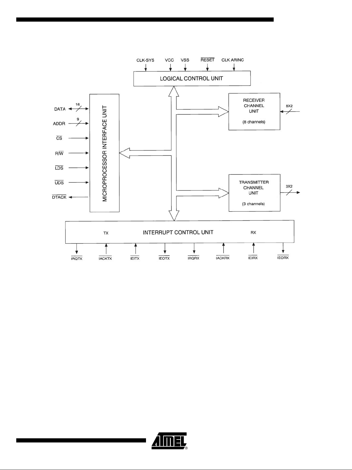
Figure 1. Simplified Block Diagram
TS68C429A
2120A–HIREL–08/02
3
Package See “Package Mechanical Data” on page 40 and “Terminal Connections” on page 41.
Figure 1. Signal Description
Pin Name Type Function
A0-8 I Address bus . The address bus is used to select one of the internal registers during a processor
read or write cycle.
D0-15 I/O This bi-directional bus is used to rece ive data from or transmit d ata to an intern al register during a
processor read or wri te c ycle. Du ring an in terru pt ac k now l edg e cy cl e, th e ve ctor number is given
on the lower data bus (D0 - D7).
CS
I Chip select (active low). This input is used to select the chip for internal register access.
LDS
UDS
R/W I Read/write. This input defines a data transfer as a read (high) or a write (low) cycle.
DTACK
IRQTX
IACKTX
IEITX
IEOTX
IRQRX
I Lower data strobe. This input (active low) validates lower data during R/W access (D0-D7).
I Upper data strobe. This input (active low) validates upper data during R/W access (D8-D15).
O Data transfer acknowledge. If the bus cycle is a processor read , the chip asser ts DTACK to
indicate that the information on the data bus is valid. If the bus cycle is a processor write, DTACK
acknowledges the a cceptance of the data b y the MRT. DTACK
access (CS
O Interrupt transmit request. This open drain output signals to the processor that an interrupt is
pending from the transmission part of the MRT. There are 6 causes that can generate an
interrupt request (2 per channel: FIFO emp ty and end of transm is si on).
I Interrupt transmit acknowledge. If IRQTX is active, the MRT will begin an interrupt acknowledge
cycle. The MRT will generate a vector number to the processor which is the highest priority
channel requesting interrupt service.
I Interrupt transmit enable in. This input, together with IEOTX signal, provides a daisy chained
interrupt structure for a vectored scheme. IEITX
device is requesting interrupt service.
O Interrupt transmit enable out. This output, together with IEITX signal, provides a daisy chained
interrupt structure for a vectored interrupt scheme. IEOTX
devices that neither the TS68C429A nor any highest priority peripheral is requesting an interrupt.
O Interrupt transmit request. This open drain output signals to the processor that an interrupt is
pending from the receiving part of the chip. There are 9 causes that can generate an interrupt
request (1 per channel: valid message received, and 1 for bad parity on a received message).
asserted) or interrupt acknowledge cycle (IACKTX or IACKRK asserted).
(active low) indicates that no higher priority
will be asserted during chip selec t
(active low) indicates to lower priority
IACKRX
IEIRX
IEORX
TX1H O Transmission “1” line of the channel 1.
TX1L O Transmission “0” line of the channel 1.
TX2H O Transmission “1” line of the channel 2.
TX2L O Transmission “0” line of the channel 2.
TX3H O Transmission “1” line of the channel 3.
TX3L O Transmission “0” line of the channel 3.
RX1H I Receivi ng “1” line of the channel 1.
RX1L I Receiving “0” line of the chann el 1.
RX2H I Receivi ng “1” line of the channel 2
4
TS68C429A
I Interrupt receive acknowledge. Same function as IACKTX but for receiver part.
I Interrupt receive enable in. Same function as IEITX but for receiver part.
I Interrupt receive enable out. Same function as IEOTX but for receiver part.
2120A–HIREL–08/02
Figure 1. Signal Description (Continued)
Pin Name Type Function
RX2L I Receiving “0” line of the chann el 2.
RX3H I Receivi ng “1” line of the channel 3.
RX3L I Receiving “0” line of the chann el 3.
RX4H I Receivi ng “1” line of the channel 4.
RX4L I Receiving “0” line of the chann el 4.
RX5H I Receivi ng “1” line of the channel 5.
RX5L I Receiving “0” line of the chann el 5.
RX6H I Receivi ng “1” line of the channel 6.
RX6L I Receiving “0” line of the chann el 6.
RX7H I Receivi ng “1” line of the channel 7.
RX7L I Receiving “0” line of the chann el 7.
RX8H I Receivi ng “1” line of the channel 8.
RX8L I Receiving “0” line of the chann el 8.
TS68C429A
RESET
V
/GND I These inputs supply power to the chip. The VCC is powered at +5 volts and GND is the ground
CC
CLK-SYS I The clock input is a single-phase signal used for internal timing of processor interface.
CLK-ARINC I This input provides the timing clock to synchronize received/transmitted messaged.
I This input (active low) will initialize the TS68C429A registers.
connection.
2120A–HIREL–08/02
5
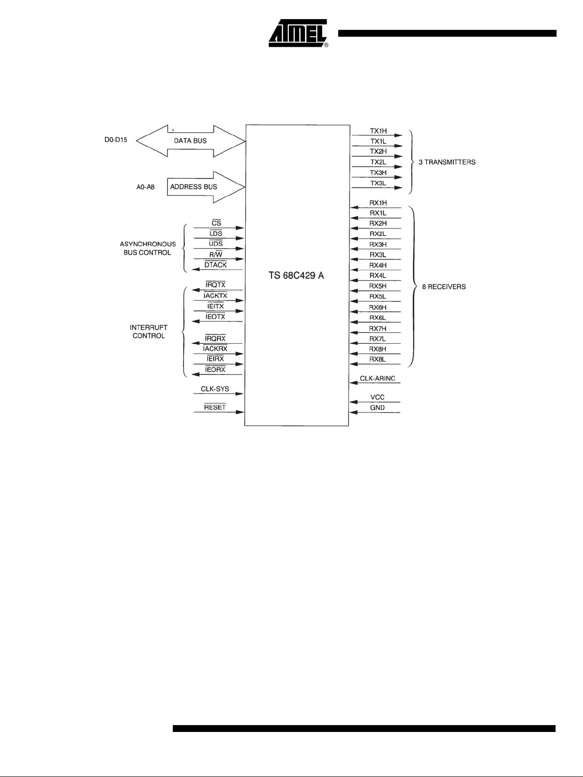
Figure 2 illustrates the functional signal groups.
Figure 2. Functional Signal Groups Diagram
Scope This drawing describes the specified requiremen ts for the ARINC multi channel
receiver/transmitter, in compliance either with MIL-STD-863 class B or SMD drawing.
Applicable Documents
MIL-STD-883 1. MIL-STD-883: test methods and procedures for electronics
2. MIL-STD-38535: general spe cifi cat ion s for micr oci rcui ts .
3. MIL-STD-1835 microcircuit case outlines.
4. DESC/SMD.
Requirements
General The microcircu its are in accordanc e with the applicabl e document and as s pecified
herein.
6
TS68C429A
2120A–HIREL–08/02
TS68C429A
Design and Construction
Terminal Connections Depending on the package, the terminal connections is detailed in “Terminal Connec-
tions” on page 41.
Package The circuits are packaged in a hermetically sealed ceramic package which is conform to
case outlines of MIL-STD 1835 (when defined):
• PGA 84,
• CQFP 132.
The precise case outlines are described at the end of this specification (“Package
Mechanical Data” on page 40) and into MIL-STD-1835.
Special R ecommended Conditions for CMOS Devices
•
The CMOS cell is basically composed of two complementary tr ansistors (a P-channe l
and an N-channel), an d, i n the ste ady s tate , onl y one trans istor i s turn ed- on . The a ct ive
P-channel transistor sources current when the output is a logic high and presents a high
impedance when the output is a logic low. Thus the overall result is extremely low power
consumption beca use ther e is no power l oss throu gh the a ctive P- channel transis tor.
Also since only once transistor is determined by leakage currents.
Because the basic CMOS cell is composed of two complementary transistors, a parasitic semiconductor controlled rectifier (SCR) formed and may be triggered when an
input exceeds the supp ly vo ltage. T he SCR that is fo rmed b y this hig h input cau ses the
device to become “latched” in a mode that may result in excessive current drain and
eventual destruction of the device. Although the device is implemented with input protection diodes, care should be exercised to ensure that the maximum input voltages
specification is not exceeded from voltage transients; others may require no additional
circuitry.
•
The TS68C429 A doesn’ t sati sfy tot ally the input/o utput d rive re quirem ents of TTL log ic
devices, see Table 4.
Electrical Characteristics
Table 1. Absolute Maximum Ratings
CMOS Latch-up
CMOS/TTL Levels
Symbol Parameter Test Conditions Min Max Unit
V
CC
V
I
P
dmax
T
case
T
stg
T
j
T
leads
2120A–HIREL–08/02
Supply Voltage -0.3 +7.0 V
Input Voltage -0.3 +7.0 V
Max Power Dissipation 400 mW
M suffix -55 +125 °C
Operating Temperature
V suffix -40 +85 °C
Storage Temperature -55 +150 °C
Junction Temperature +160 °C
Lead Temperature Max 5 sec. soldering +270 °C
7
Unless otherwise stated, all voltages are referenced to the reference terminal.
Table 2. Recommended Condition of Use
Symbol Parameter Test conditions Min Max Units
V
CC
V
IL
V
IH
Supply Voltage 4.5 5.5 V
Low Level Input Voltage -0.5 0.8 V
High Level Input Voltage 2.25 5.8 V
M suffix -55 +125 °C
T
case
C
L
t
(c) Clock Rise Time (See Figure 3) 5 ns
r
t
(c) Clock Fall Time (See Figure 3) 5 ns
f
f
c
Operating Temperature
V suffix -40 +85 °C
Output Loading Capacita nce 130 pF
Clock System Frequency
(See Figure 3)
0.5 20 MHz
This device contains protective circuitry against damage due to high static voltages or
electrical fields: however, it is advised that normal precautions be taken to avoid application of any voltages hig her than maximum-rated vol tage s to this hi gh-i mpe dan ce circuit.
Reliability of operation is enhanced if unused inputs are tied to an appropriate logic voltage level (e.g., either GND or VCC).
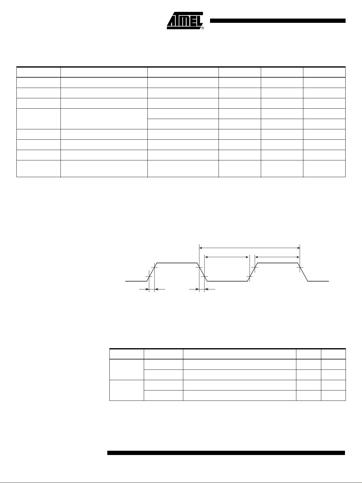
Figure 3. Clock Input Timing Diagram
t
cyc
t
CL
t
CH
2.25V
0.8V
t
CR
t
CF
Note: Timing measurements are referenced to and from a low of 0.8-volt and a high voltage of
2.25 volts, unless otherwise noted. The voltage swing through this range should start
outside and pass through the range such that the rise or fall will be linear between
0.8-volt and 2.25 volts.
Table 3. Thermal Characteristics
Package Symbol Parameter Value Unit
PGA 68
CQFP 132
θ
J-A
θ
J-C
θ
J-A
θ
J-C
Thermal Resistance Jun c tion-to-ambient 28 °C/W
Thermal Resistance Junction-to-case 2 °C/W
Thermal Resistance Jun c tion-to-ambient 27 °C/W
Thermal Resistance Junction-to-case 3 °C/W
8
TS68C429A
2120A–HIREL–08/02

TS68C429A
Power Considerations The average chip-junction tempe ra tur e, TJ, in °C can be obtained from:
T
= TA + (PD ⋅ θJA)(1)
J
T
= Ambient Temperature, °C
A
θ
= Package Thermal Resistance, Junction-to-Ambient, °C/W
JA
P
= P
D
P
INT
P
I/O
For most application s P
An approximate relationship between P
Solving equations (1) and (2) for K gives:
where K is a constant pertaining to the particular part K can be determined from equation (3) by measuring P
values of P
value of T
The total thermal res istance of a pack age ( θ
θ
JC
package (case), surface (θ
terms are related by the equation:
θ
JC
dent and can be minimized by such thermal management techniques as heat sinks,
ambient air cooling and thermal co nvection. Thu s, good thermal managemen t on the
part of the user can significantly reduce θ
tution of θ
temperature.
+ P
INT
I/O
= ICC x VCC, Watts—Chip Internal Power
= Power Dissipation on Input and Output Pins—User Determined
< P
I/O
P
= K: (TJ + 273) (2)
D
K = P
⋅ (TA + 273) + θJA ⋅ P
D
and TJ can be obtained by sol ving equ ations (1) and (2) it erativ ely for an y
D
.
A
D
and can be neglected.
INT
and TJ (if P
D
2
D
is neglected) is:
I/O
(3)
(at equilibriu m) for a known TA. Using this value of K, the
) can be separated into two components,
JA
and θCA, representing the barrier to heat flow from the semiconductor junction to the
) and from the case to the outside ambient (θCA). These
JC
θ
= θJC + θ
JA
CA
(4)
is device related and cannot be influenced by the user. However, θCA is user depen-
so that θJA approximately equals θJC. Substi-
for θJA in equation (1) will result in a lower s emiconductor junction
JC
CA
Mechanical and Environment
The microcircuits shall meet all mechanical environmental requirements of either MILSTD-883 for class B devices or DESC devices.
Marking The document where are defined the marking are identified in the related reference doc-
uments. Each mic rocircuit are legib ly and permanentl y marked with the follow ing
information as minimum:
•Atmel logo
• Manufacturer’s part number
• Class B identification
• Date-code of inspection lot
• ESD identifier if available
• Country of manufacturing
2120A–HIREL–08/02
9
Quality Conformance Inspection
DESC/MIL-STD-883 Is in accordance with MIL -M-3851 0 and met hod 50 05 of MIL-S TD-883 . Grou p A and B
inspections are performed on each production lot. Group C and D inspections are performed on a periodic basis.
Electrical Characteristics
General Requirements All static and dynamic electrical characteristics specified for inspection purposes and the
relevant measurement conditions are given below:
• Table 4, Table 5: Static electrical characteristics for the electrical variants.
• Table 6, Table 7, Table 8: Dynamic electrical characteristics.
For static characteristics (Table 4, Table 5), test methods refer to IEC 748-2 method
number, where existing.
For dynamic characteristics (Table 6, Table 7, Table 8), test methods refer to clause 5. 5
of this specification.
Table 4. DC Electrical Characteristics
With -55
°C ≤ T
≤ +125°C or -40° ≤ T
case
≤ +85°C; VCC = 5V ± 10%.
case
Symbol Parameter Min Max Unit
V
IH
V
IL
V
OH
V
OL
I
OH
I
OL
I
LI
IDD Dynamic Current
Input High Voltage 2.25 VCC + 0.3 V
Input Low Voltage -0.5 0.8 V
Output High Voltage (exc ep t IR QRX, IRQTX: open drain outputs) 2.7 V
Output Low Voltage 0.5 V
Output Source Current (except IRQRX,
: open drain outputs)
IRQTX
Output Sink Current (V
= 2.7V) -8 mA
(V
out
= 0.5V) 8 mA
out
Input Leakage Current (Vin = 0 to VCC) ±20 µA
(T
= T
(1)
case
min
= V
⋅ V
max
DD
)
65 mA
Note: 1. IDD is measured with all I/O pins at 0V, all input pins at 0V except signals CS, IACKxx, LDS, UDS at 5V and CLK-SYS and
CLK-ARINC which run at t
cyc
mini.
Table 5. Capacitance (TA = 25°C)
Symbol Parameter Max Unit
C
in
C
out
Input Capacitance 10 pF
HI-Z Output Capacitance 20 pF
10
TS68C429A
2120A–HIREL–08/02
Clock Timing
Table 6. Clock System (CLK SYS)
Symbol Parameter Min Max Unit
t
S Clock Period 50 2000 ns
cyc
t
, t
CLS
CHS
t
, t
crS
cfS
Table 7. Clock ARINC (CLK ARINC)
Symbol Parameter Min Max Unit
t
ACycle Time
cyc
t
, t
CLA
CHA
t
, t
crA
cfA
Note: 1. t
A ≥ 4 x t
cyc
cyc
S.
Clock Pulse Width 20 ns
Rise and Fall Times 5 ns
Clock Pulse Width 240 ns
Rise and Fall Times 5 ns
TS68C429A
(1)
200 8000 ns
AC Electrical Characteristics
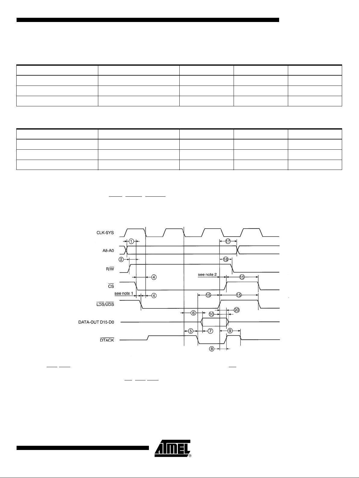
Figure 4. Read Cycle
With VCC = 5 VDC ± 10% VSS = 0 VDC.
IEIxx
, IEOxx, IACKxx, must be understood as generic signals (xx = RX and TX).
Notes: 1. LDS/UDS can be asserted on the next or previous CLK-SYS period after CS goes low but (4) must be met for the next
period.
2. The cycle ends when the first of CS
, LDS/UDS goes high.
11
2120A–HIREL–08/02
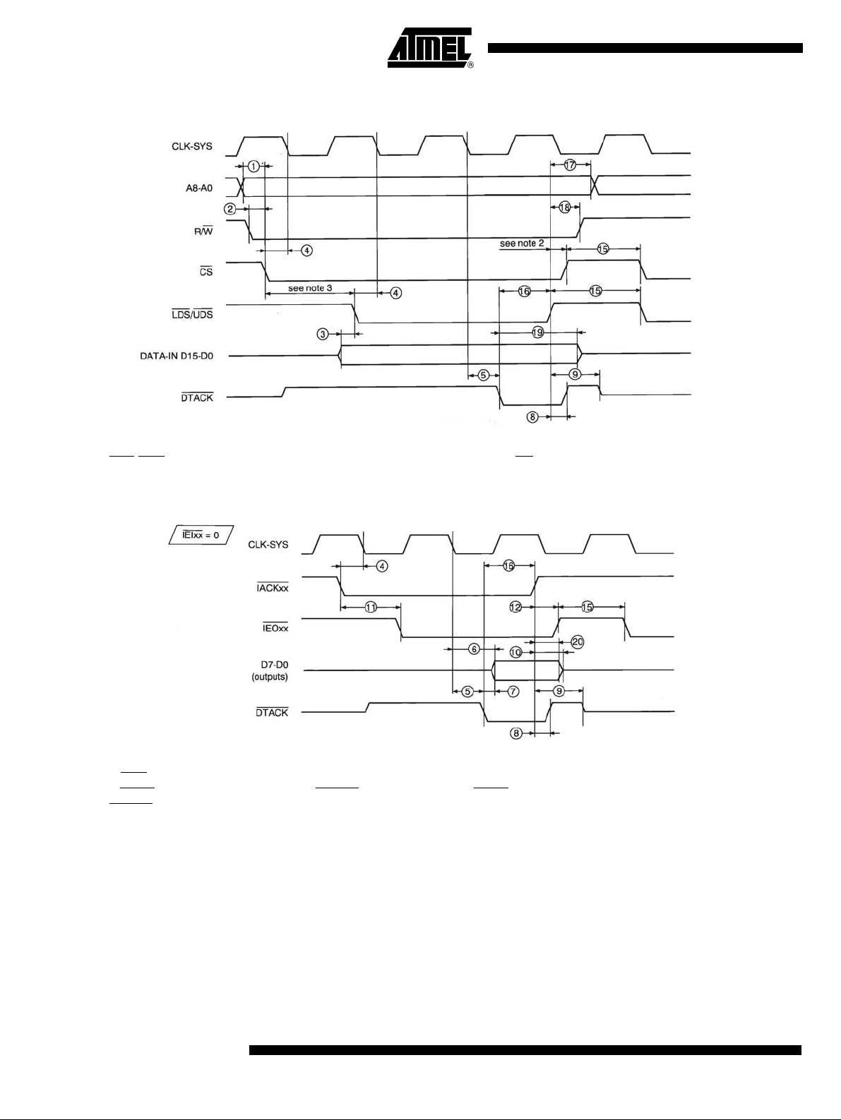
Figure 5. Write Cycle
3. LDS/UDS can be asserted on the same or previous CLK-SYS period as CS but (3) and (4) must be met.
Figure 6. Interrupt Cycle (IEIxx = 0)
Notes: 1. If UDS = 1, D15-D8 stay hi-z else D15-D8 drive the bus with a stable unknown value.
12
2. If IEOxx
DTACK
TS68C429A
goes low, neither ve cto r nor DTAC K are generate d, els e IEOxx stays inactive and a vector is generated (D7-D0 and
).
2120A–HIREL–08/02
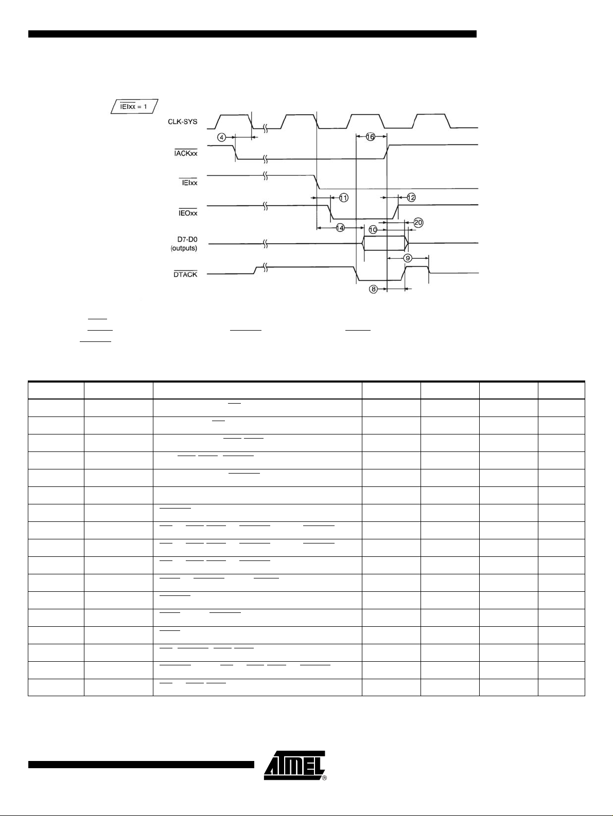
Figure 7. Interrupt Cycle (IEIxx = 1)
Notes: 1. If UDS = 1, D15-D8 stay hi-z else D15-D8 drive the bus with a stable unknown value.
2. If IEOxx
DTACK
goes low, neither ve cto r nor DTAC K are generate d, els e IEOxx stays inactive and a vector is generated (D7-D0 and
).
TS68C429A
Table 8. Timing Characteristic
Number Symbol Parameter Min Max T/G
1t
2t
3t
4t
5t
6t
7t
8t
9t
10 t
11 t
12 t
13 t
14 t
15 t
16 t
17 t
AVCSL
RWVCSL
DIVDSL
SVCL
CLDKL
CLDOV
DKLDOV
SHDKH
SHDXZ
SHDOZ
ILIOL
IKHIOH
IILDKL
IILDOV
SH
DKLSH
SHAH
Address valid to CS low 0 - T ns
R/W valid to CS low 0 - T ns
Data in valid to LDS/UDS low 0 - T ns
CS, LDS/UDS, IACKxx valid to CLK-SYS low 5 - T ns
CLK-SYS low to DTACK low - 45 T ns
CLK-SYS low to data out valid - 50 T ns
DTACK low to data out valid - 10 G ns
CS or LDS/UDS or IACKxx high to DTACK high - 35 G ns
CS or LDS/UDS or IACKxx high to DTACK hi-z - 50 G ns
CS or LDS/UDS or IACKxx high to data out hi-z - 25 G ns
IEIxx or IACKxx low to IEOxx low - 35 T ns
IACKxx high to IEOxx h igh - 40 T ns
IEIxx low to DTACK low - 40 T ns
IEIxx low to data out valid - 45 T ns
CS, IACKxx, LDS/UDS inactive time 15 - T ns
DTACK low to CS or LDS/UDS or IACKxx high 0 - G ns
CS or LDS/UDS high to address hold time 0 - G ns
(1)
Unit
2120A–HIREL–08/02
13

Table 8. Timing Characteristic (Continued)
Number Symbol Parameter Min Max T/G
(1)
Unit
18 t
19 t
20 t
Note: 1. T/G = Tested/Guaranteed.
SHRWI
DKLDIH
SHDOH
CS or LDS/UDS high to R/W invalid 0 - G ns
DTACK low to data in hold time 0 - G ns
CS or LDS/UDS or IACKxx high data out hold
time
0-Gns
Functional Description
Receiver Channel Unit (RCU)
Overview The RCU is composed of 8 ARINC receiver channels and has per channel:
• a serial to parallel converter to translate the two serial signals in two 16-bit words.
• a memory to store the authorized labels,
• a control logic to check the validity of the received message.
• a buffer to keep the last valid received message.
Inputs Each receiver channel has two input lines, receiving line high (RxiH) and receiving line
low (RXiL) which are not directly compatible with the bipolar modulated ARINC line. This
ARINC three-level s tate signal s (“HIGH” , “NULL”, “LO W”) shou ld be de multiple xed to
generate the two RZ lines according to Figure 8.
Figure 8.
Description Each channel h as a test mo de in which th e input sign als (RXiH , RXiL), ar e internal ly
connected to the third Transmit Channel Lines. This selection is done by programming
the Test bit in the recei ver control regis ter (see “Registe r Descriptio n” on page 17)
except this difference, the TS68C429A behaves exactly the same manner in the two
modes. The receiver channel block diagram is given in Figure 9.
ARINC signals being asynchronous, the RCU first rebuilds the received clock in order to
transfer the dat a withi n the shif t-regi ster an d when th e Gap-c ontrol ler has detec ted the
end of the message, tests the message validity according to the criteria listed hereafter.
14
TS68C429A
2120A–HIREL–08/02

TS68C429A
To detect the end of the me ssage, the Gap-Con troller waits for a G ap after the last
received bit. To do so, at each CLK ARINC cycle, a counter is inc remented and compared to the content of the Gap- Register which has th e user pro gramm ed value. If bo th
values are equal, the counter is stopped and an internal end of message signal is generated. This counter is re seted on the falling edge of the rebuil t cloc k. Fi gure 9 show s the
gap detection principle.
When the end of message is detected, the TS68C429A verifies the following points:
• the number of received bits must be 32,
• if requested the message parity (see “Register Description” on page 17) is
compared to the parity bit of the message,
• the message label must be equal to one of the label stored in the Label Control
Matrix,
• the Buffer is empty (that is: the last message has been read). The corresponding bit
in the Status-register (see logical interface unit), has been cleared,
• when all four conditions are met, the message is transferred from the Shift-register
to the Buffer and the corresponding bit is set in the Status-register. If the interrupt
mode is enabled (see “General Circuit Control” on page 24) the IRQRX line is
activated.
If not, reception of a new message is enabled, see Note.
If only the message parity is incorrect, an interrupt can be generated (see “Register
Description” on page 17).
The Buffer is seen as two 16-bit word registers, the Most Significant Word of the mes-
sage (MSW) is contained in the lower address, the Less Significant Word of the
message (LSW) is contained in the upper address. The MSW should be read first
because reading the LSW will release the buffer and allow transfer of a new message
from the Shift-register.
2120A–HIREL–08/02
15

Figure 9. Receiver Channel Block Diagram
Note: A valid message is stored in the Shift-Reg. until a new message arrives and so may be transferred to the message buffer as
soon as the buffer is “freed”.
16
TS68C429A
2120A–HIREL–08/02

Figure 10.
Rebuilt clock
CLK-ARINC
Gap register
TS68C429A
Synchro counter
End of msg
Register Description Four registers are associated to each receiver channel. These four registers are:
a) receiver control
b) gap register
c) message buffer
d) label control matrix
Register Control Register
•
This read/write register controls the function of the related receiver channel:
2120A–HIREL–08/02
17

Figure 11.
The lowest value will give the highest pri ority. If two channels have the same pri ority,
one of them will never be able to send its interrupt vector to the microprocessor. Each
channel must have a unique channel priority order.
USD access LDS access
1514131211109876543210
Channel priority order
Not used
Wrong parity
Not used
Parity control
Label control matrix write enable
Label control
Test mode
Channel enable
Table 9. Register Control Register Description
Bit Function Comments
Bit 15 Channel enable 0: channel is out of service
1: channel is in service
Bit 14 Test mode 0: external ARINC lines as input (normal operation)
1: third transmitter lines as input (test mode)
Bit 13 Label control 0: no control, all the labels are accepted
1: automatic check of the label according to the label control matrix
Bit 12 LCMWE label control matri x
write enable
Bit 11 Parity control 0: even parity check
Bit 10 Parity control 0: parity check is disable
Bit 9 Not used
Bit 8 Not used
Bit 7 Wrong parity: this feature is
enabled only if the self-test
register bit 0 is set 1
0: receiving mode (write to the matrix are disabled)
1: programmation mode for labels control matrix
1: odd pari ty check
1: parity check is enable
0: received message p arity is corr ect if read, res et wrong w rong pari ty flag i f writte n.
1: an incorrect received message parity has been detected (the corresponding
message is lost) (set by hardware).
Bit 6 Not used
18
TS68C429A
2120A–HIREL–08/02

TS68C429A
Table 9. Register Control Register Description
Bit Function Comments
Bit 5 Not used
Bit 4 Not used
Bit 0 to 3 Channel priority: order The lowest value will give the highest priority. Each channel must have a unique
channel priority order.
If several messa ges are pending, the inter rupt vect or will account fo r highes t priority
channel.
• Gap Register (Figure 12)
The gap register is acc es sibl e fo r w ritin g op er ati ons on ly . It c on tai ns the v alue o n wh ich
the gap counter will be stopped and will generate the end of the m essage signal (s ee
“Inputs” on page 14). The value is interpreted as a multiple of the CLK ARINC period.
Figure 12. Gap Register Description
The value of the gap register must be chosen so as to generate the end of the message
before the minimal gap as defined in the ARINC-429 norm.
•
Message Buffer
The Buffer is made of two 16-bit regis ters, th e Most Sign ificant Word of the messag e
(MSW) is contained in the lower address register, the Least Significant Word of the message (LSW) is contained in the upper address register. For correct behavior, the MSW
must be read before the LSW. They are accessible in read mode only and 16-bit access
is mandatory.
•
Label Control Matrix
The label control matrix is a 256 x 1 bit memory. There is one memory per channel.
The address is driven by the incoming label, the output data is used to validate this
incoming message label (see Figure 13). To program this matrix, the LCMWE (label
control matrix write enable) bit of the receiver-control-register should be set to “1” to
allow the access. At this time, the address is driven by the external address bus and the
data are written from the data bus D7 to D0 (one per channel according to Figure 14).
Any write to a matri x on wh ich the LC MWE i s not s et will n ot hav e any e ffect. Th e labe l
control matrix can be wr i tten or r ea d i n byte a nd wor d mod e. In wor d m ode , th e sta te of
D15-D8 is unknown. After complete programming of the matrix, the LCMWE bit should
be reset to “0” to allow normal receiving mode. A “1” in the memory means that this label
is allowed and a “0” means that this label must be ignored.
2120A–HIREL–08/02
19

Figure 13. Label Control Matrix
Figure 14.
Transmitter Channel Unit (TCU)
Overview The TCU is composed of three ARINC transmit channels and has per channel:
• a parallel to serial converter to translate the messages into two serial signals,
• a FIFO memory to store eight 32-bit ARINC messages,
• a control logic to synchronize the message transmitter (parity, gap, speed...).
Outputs Each transmitter channel has two output lines, Transmit line High (TXiH) and Transmit
line Low (TXiL) which are not directly compatible with the bipolar modulated ARINC line.
These RZ format lines should be translated by an outside device into ARINC three-level
state signal according to Figure 15.
20
TS68C429A
2120A–HIREL–08/02

TS68C429A
Figure 15. Transmitter Channel Unit Outputs
Description The block diagram of a tran smit channel is given is given in Figure 16. Only the thi rd
channel can be switched to internal lines for test mode, otherwise the channels are identical. The selection of this test mode is d one by programming the test bit in the
transmitter-control-reg ister (see “Regist er Descripti on” on page 1 7). In this te st mode
the lines TX3H and TX3L are not driven, they are both kept at “0”.
The transmit frequency is generated by dividing the ARINC clock signal (CLK ARINC)
by the value con tained in the frequency r egister. T his divide d clock syn chronize s the
shift register which sends the 32-bit word on the lines TXiH and TXiL.
The parity is computed and if requested (see “Register Description” on page 17) the parity bit (32nd bit of the message) is modified to have an odd number of “1” in the 32-bit
message for odd parity or an even number of “1” in the 32-bit message for even parity.
A gap control block gene rates a ga p be twee n the sent messages. The val ue of this ga p
is defined by the 5 bits “transmission gap” of the transmitter-control-register, it is given in
number of ARINC bit (see “Register Description” on page 17).
A FIFO control block manages the messages to be sent. Up to 8 messages can be written into the FIFO. The FIFO is seen as a two 16-bit memory words, the Most Significant
Word of the message (MS W ) is written in the lower addre ss , th e Le ast Si gni fi ca nt W ord
of the message (LSW) is wr it ten i n th e up per ad dres s. The MSW should be written first.
The access to the FIFO is 16 bits mand atory . The number of messages within the FIFO
is indicated by a counter that can be read through the transmitter-control-register. This
counter is incremented when the LSW is written and decremented when the message is
transferred to the s hift- regi ste r. The “ Res et FIF O” bi t i s us ed to c ancel me ss ag es withi n
the FIFO. If a transmission is on going, the entire messag e will be sent. The “reset
FIFO” bit remains active until written at 1 by the microprocessor. When the transmitter is
disable during a transmission, the out going message is lost.
When the FIFO is empty , a b it i s set in t he s tatu s- regi s ter ( se e “Ge ner al Cir c uit Control”
on page 24). If the interrupt mo de is ena ble d (see “Gene r al Ci rcui t Cont rol” on pag e 24)
the IRQTX
line is activated.
2120A–HIREL–08/02
When the transmitter FIFO is empty and when no transmission is on going, the first write
access to the FIFO has to be preceded by the following sequence: disable and enable
transmission (see Figure 36: First FIFO access).
21

Figure 16. Transmitter Channel Block Diagram
Register Description Three registers are associated to each transmitter channel:
• the frequency register,
• the transmitter control register,
• the FIFO.
The Frequency Register
•
The frequency register is only accessible for writing operations by the user and contains
the frequency divider.
Figure 17. Frequency Register
22
TS68C429A
2120A–HIREL–08/02

The transmission fr equ enc y c an be c om pute d by div iding the CLK ARINC frequ enc y by
the frequency register value.
The frequency register must be loaded with a value greater or equal to 2.
The Transmitter Control Register
•
The transmitter control register is accessible for reading and writing operations.
Figure 18. Transmitter Control Register
TS68C429A
Table 10. Transmission Control Register Description
Bit Function Comments
Bit 15 Enable transmission - 0: channel out of service (stops on going transmission)
- 1: channel in service
- 1 to 0: transition is not allowed at the same time as an 1 to 0 transition of the bit 4
- when the transmitte r FIFO is e mpty and when no tran smissi on is on g oing, the first
write access to the FIFO has to be preceded by the following sequence: reset to 0
and then set to 1
Bit 14 Test (only 3rd channel) 0: normal operating
1: test, output are only driven on internal lines for input testing
Bit 13 to 12 Not used
Bus 11 Parity control 0: even parity calculation
1: odd parity calculation
Bit 10 Parity control 0: parity disable, Bit 32 of the message stays unchanged
1: parity enable. Bit 32 of the message will be forced by parity control
Bit 9 to 5 Transmission gap “transmission gap” which is the delay between two 32-bit ARINC messages (in
ARINC bit)
Bit 4 Reset FIFO - write a 0 in this bit reset the FIFO counter
- this bit must be set to 1 before any write in the transmit buffer.
- 1 to 0: transition is not allowed at the same time as an 1 to 0 transition of the bit 15
Bit 3 to 0 Number of msg these four bits indicate the available space within the FIFO
2120A–HIREL–08/02
23

• FIFO
The FIFO is seen as two 16-bit words. Th e Most Significan t Word (MSW) mus t be writ-
ten first. The Least Significant Word (LSW) write increments the FIFO counter.
Before any write, the user should verify that the FIFO is not full. If the FIFO is full, any
write to the FIFO will be lost.
General Circuit Control
Logical Control Unit (LCU) The LCU mainly distributes the clocks and reset within the MRT. The reset signal, active
low is an asynchron ous sign al . Wh en i t oc cu r s, all re gist e rs ar e res et t o z er o ex ce pt th e
Label-Control-Matrix which is not initialized and the Status-Register which is set to FC00
(hex). Reset duration must be greater than 4 clk-cyc periods.
The LCU contains the St atus-reg ister. This read/writ e register indica tes the state of th e
internal operations. It i s a lso th e im age of the pending interrupts if the y ar e not m aske d.
Clearing a bit “RX-Chann el-i” will cancel the re ceived messag e and release the Me ssage-buffer for reception of a ne w message. The “En d of TX on channel-i” Is set only
when the involved chan nel FIFO is empt y. The format of the Stat us-Regist er is given
below.
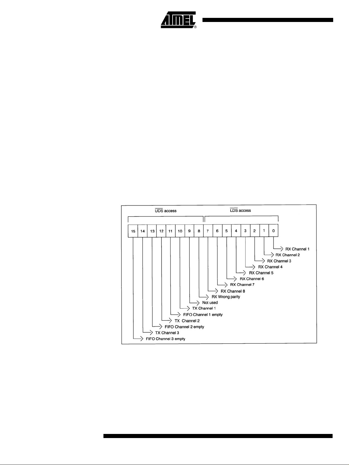
Figure 19. Status Register
24
TS68C429A
2120A–HIREL–08/02

Table 11. Description of LCU Status Register
Bit Function Comments
Bit 15, 13, 11 FIFO channel 3, 2, 1 empty 0: FIFO not empty
1: FIFO empty
Bit 14, 12, 10 End of transmission on channel 3, 2, 10: Transmission occurs
1: No transmission actually
TS68C429A
Bit 8 RX wrong parity. This feature is
available only if self-test register bit 0
is set to 1. This bit must be reset to 0
by user when needed.
Bit 7, 6, 5, 4, 3, 2, 1, 0 Receiving cha nne l 8, 7, 6, 5, 4, 3, 2, 1 0: Waiting for message
Microprocessor Interface Unit (MIU)
This interface which is directly compatible with the Atmel TS68K family is based on an
asynchronous data transfer .
0: No wrong parity received
1: At least one receiver has received a message with wrong
parity (set by hardware).
1: Received corr ect message
The data exchange is mandatory on 16 bits for access to the FIFO messages (transmitter) and to the message buffer (receiver). For other access it can be on byte on D0-D7
with LDS assertion or an D8-D15 with UDS assertion.
Figure 20 and Figure 21 show the read and write flow chart.
Figure 20. Read Cycle Flow Chart
2120A–HIREL–08/02
25
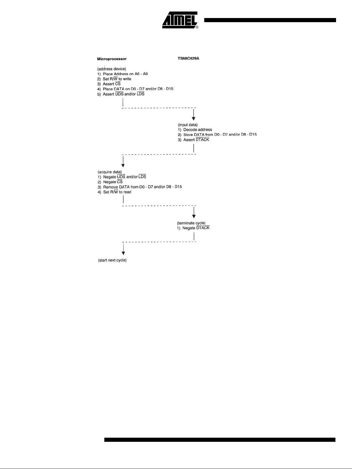
Figure 21. Write Cycle Flow Chart
Interrupt Control Unit (ICU) •
26
TS68C429A
Daisy Chain
The ICU is composed of 2 interrupt blocks with a daisy chain capabilit y (transm itter and
receiver blocks). The daisy chain allows more than one circuit to be connected on the
same interrupt li ne. Figure 22 shows the use of a daisy cha in. IRQxx, IAC Kxx, IEIxx ,
IEOxx must be understood as generic signals. They are IRQTX, IACKTX, IEITX, IEOTX
for the transmitter block and IRQRX, IACKRX, IEIRX, IEORX for the receiver block.
If IEIxx = 0, no higher device have an interrupt pending on the same line so the interrupt
is requested and the IEOxx is for ced high to disable lowest devices to generate interrupt. If IEIxx = 1, it waits for the condi tion IEIxx = 0. When IEIxx is tie d high, IEO xx is
forced high.
The daisy chains can be use d to program a pr iority betwee n receive rs and trans mitters
interrupts when only one interrupt level is needed. An example is given in “Microprocessor Interface” on page 33.
2120A–HIREL–08/02

Figure 22. Interrupt Control Unit Daisy Chain Use
Vectored Interrupt
•
They are 15 possibilities to generate an interrupt and two lines to handle them. To be
more efficient, a unique vector number for each cause is given to the microprocessor as
an answer to an IRQ. Figure 23 shows the interrupt acknowledge sequence flow chart.
TS68C429A
Figure 23. Interrupt Acknowledge Sequence Flow Chart
2120A–HIREL–08/02
27
• Register Description
Any internal status change that induces a bit to be set in the status-register will generate
an interrupt if this cause is ena ble d by the Mas k -re gis ter and if no hi ghe st pri ority ca us e
is already activated or pending.
For the receiver blocks, the priority is programmable (see interrupt vector number
description). For the transmitter block, the End-of-transmission has higher priority than
FIFO-empty and channel 1 has higher priority than channel 2 that has higher priority
than channel 3.
The RX wrong parity bit can be set only if self-test register bit 0 is set to 1.
The user has to check which receiver has it receiver control register bit 7 set to 1.
At the end of the interrupt procedure, the user must reset RX wrong parity bit to 0.
RX wrong parity is the highest interrupt priority source for the receiver part of the MRT.
•
The Mask Register
The mask register is acc es sibl e for read ing and wr it ing oper a tion s. Th e mask reg ist er is
used to disable interrupt source. The bit order is the same as in the status register. A “0”
indicates that this source is disable, a “1” enables an interrupt for this source.
Figure 24. Mask Register
28
TS68C429A
The Base Register
•
The base register is only accessible for writing operations by the user. The base register
must be programmed at the init ializati on ph ase. It conta ins t he base for th e vector generation during an interrupt acknowledge. T his allows the use of severa l peripherals. If
not programmed interrupt vector is set to $OF.
2120A–HIREL–08/02
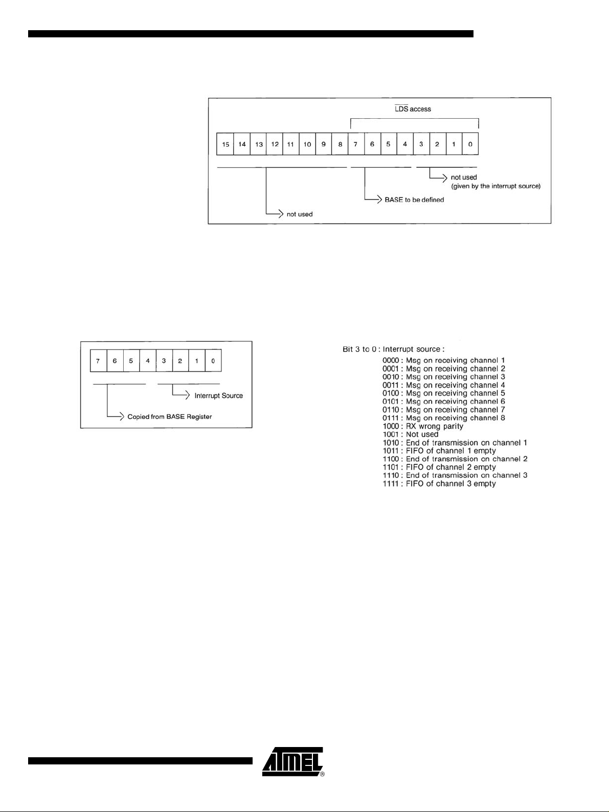
Figure 26.
TS68C429A
Figure 25. Base Register
The Interrupt Vector Number
•
During an i nter rup t a cknow ledg e cy cle, an 8- bi t vect or n umb er is pr esen ted t o t he mic ro -
processor on D0-D7 lines. This vector number corresponds to the interrupt source
requesting service. The format of this number is given below.
Self-test Description A self-test has been im plemented for the r eceiver control label matrix RAM and the
transmitter FI FO. This te st can be u sed to g uaran tee t he g ood behav ior of th e di ffer ent
MRT’s memories.
29
2120A–HIREL–08/02

Register Description Figure 27. Self-test Register
The self-test register can be split in three parts :
1. bit 0: Used to enable receiver wrong parity detection. This bit has been implemented to guarantee compatibility with previous designs:
0: Receiver wrong parity detection disable,
1: Receiver wrong parity detection enable.
2. Self-test command:
bit 5: Receiver test clock mode:
0: If CLK-SYS is less or equal to 10 MHz,
1: If CLK-SYS is higher than 10 MHz.
bit 6: Start transmit ter self-t est if a 0 to 1 transit ion is progra mmed (before a new
self-test, the user must reprogram this bit to 0).
bit 7: Start receiver Label Control Matrix self-test if a 0 to 1 transition is programmed
(before a new self-test, the user must reprogram this bit to 0).
3. Self-test result:
bit 8: 0: Transmitter 1 self-test is running,
1: End of Transmitter 1 self-test.
bit 9: 0: Transmitter 2 self-test is running,
1: End of Transmitter 2 self-test.
bit 10: 0: Transmitter 3 self-test is running,
1: End of Transmitter 3 self-test.
bit 11: Result of Transmitter 1 self-test:
0: (if bit 8 is set to 1) self-test pass,
1: Self-test fail.
bit 12: Request of Transmitter 2 self-test:
0: (if bit 9 is set to 1) self-test pass,
30
TS68C429A
2120A–HIREL–08/02

TS68C429A
1: Self-test fail.
bit 13: Result of Transmitter 3 self-test:
0: (if bit 10 is set to 1) self-test pass,
1: Self-test fail.
bit 14: 0: Receiver Label Control Matrix self-test is running,
1: End of receiver Label Control Matrix self-test.
bit 15: Result of receiver LCM self-test:
0: (if bit 14 is set to 1) self-test pass,
1: Self-test fail.
Self-test U se The self-test destroys the content of the tested memory. So, it could be used after sys-
tem reset, duri ng system initial ization. O nly one sel f-test (tra nsmitte rs and rec eivers)
can be performed aft er a res et . If the self-test must be re st ar ted, the re se t m ust be ac tivated (then released) before the new self-test start.
To program the self-test:
1. If the receiver self-test will be used:
set to 1 LCMWE bits (for all receivers).
2. If receiver self-test will be used and CLK-SYS is > 10 MHz:
set to self-test register bit 5.
3. Start self-test:
set to 1 self-test register bit 6 for Transmitter test,
set to 1 self-test register bit 7 for Receiver RAM test.
At this point, self-test is running. The test duration is:
710 CLK-SYS periods for Transmitter self-test,
2820 CLK-SYS periods for Receiver RAM test if self-test register bit 5 is 0,
5640 CLK-SYS periods for Receiver RAM test if self-test register bit 5 is 1.
Memory MAP
Address Access Register
0H
1H
2H
3H
4H
5H
6H
7H
2120A–HIREL–08/02
To read the self-test result, the user must:
1. poll the self-test register and wait for an end of test set to 1 (bits 8 to 10, bit 14)
then,
2. read the self-test register again to have a valid result on bits 11, 12, 13, 15
according to the tests which end at point 1.
R/W
W
R
R
R/W
W
R
R
Receiver-control-register
Gap-register
Message-buffer MSW
Message-buffer LSW
Receiver-control-register
Gap-register
Message-buffer MSW
Message-buffer LSW
Receiving channel 1
Receiving channel 2
31

Memory MAP (Continued)
Address Access Register
8H
9H
AH
BH
CH
DH
EH
FH
10H
11H
12H
13H
14H
15H
16H
17H
18H
19H
1AH
1BH
1CH
1DH
1EH
1FH
R/W
W
R
R
R/W
W
R
R
R/W
W
R
R
R/W
W
R
R
R/W
W
R
R
R/W
W
R
R
Receiver-control-register
Gap-register
Message-buffer MSW
Message-buffer LSW
Receiver-control-register
Gap-register
Message-buffer MSW
Message-buffer LSW
Receiver-control-register
Gap-register
Message-buffer MSW
Message-buffer LSW
Receiver-control-register
Gap-register
Message-buffer MSW
Message-buffer LSW
Receiver-control-register
Gap-register
Message-buffer MSW
Message-buffer LSW
Receiver-control-register
Gap-register
Message-buffer MSW
Message-buffer LSW
Receiving channel 3
Receiving channel 4
Receiving channel 5
Receiving channel 6
Receiving channel 7
Receiving channel 8
20H
21H
22H
23H
24H
25H
26H
27H
28H
29H
2AH
2BH
40H R/W Status-register
41H
42H
43H
100H to 1FFH R/W Label-control-matrix Receiving channels 1-8
R/W
W
W
W
R/W
W
W
W
R/W
W
W
W
R/W
W
R/W
Transmit-control-register
Frequency-register
Message-FIFO MSW
Message-FIFO LSW
Transmit-control-register
Frequency-register
Message-FIFO MSW
Message-FIFO LSW
Transmit-control-register
Frequency-register
Message-FIFO MSW
Message-FIFO LSW
Mask-register
Base-register
Self-test register
Transmission channel 1
Transmission channel 2
Transmission channel 3
MRT address 2CH to 3FH and 44H to FFH do not generate DTACK signal (illegal
address).
32
TS68C429A
2120A–HIREL–08/02

Application Notes (for additional details order the AN 68C429A)
Microprocessor Interface
Figure 28. Typical Interface with TS68000
TS68C429A
2120A–HIREL–08/02
(*) This kind of application can also work with an independant clk
33

Figure 29. Typical Interface with 68020/CPU 32 Core Microcontrollers
34
TS68C429A
2120A–HIREL–08/02

Figure 30. Typical Interface with 68302
TS68C429A
In this example, receiver interrupts have a higher priority than transmitter interrupts.
2120A–HIREL–08/02
35

Programs Flow-chart
Figure 31. Initialization after Reset Flow-chart
36
TS68C429A
2120A–HIREL–08/02

Figure 32. Receiver without Interrupt Flow-chart
TS68C429A
Figure 33. Receiver with Interrupt Flow-chart
IT START
Read "MSW"
Read "LSW"
IT END
2120A–HIREL–08/02
37

Figure 34. Transmitter without Interrupt Flow-chart
Figure 35. Transmitter with Interrupt Flow-chart
38
TS68C429A
2120A–HIREL–08/02

Figure 36. First FIFO Access
TS68C429A
Preparation for Delivery
Packaging Microcircuits are prepared for delivery in accordance with MIL-I-38535 or DESC. Certificate of Complianc e Atmel offers a certif icate of co mplianc e with each shipment of parts, affir ming the prod-
ucts are in compliance either with MIL-STD-883 or DESC and guaranteeing the
parameters not tested at temperature extremes for the entire temperature range.
Handling MOS devices must be handled with certain precautions to avoid damage due to accu-
mulation of static charge. Input protection devices have been designed in the chip to
minimize the effect of this static buildup. However, the following handling practices are
recommended:
• Devices should be handled on benches with conductive and grounded surfaces.
• Ground test equipment, tools and operator.
• Do not handle devices by the leads.
• Store devices in conductive foam or carriers.
• Avoid use of plastic, rubber, or silk in MOS areas.
• Maintain relative humidity above 50 percent if practical.
2120A–HIREL–08/02
39

Package Mechanical Data
PGA 84
CQFP 132
40
TS68C429A
2120A–HIREL–08/02

Terminal Connections
84-lead PGA Assignment
TS68C429A
132-lead CQFP Assignment
2120A–HIREL–08/02
41
Ordering Information
Standard Product
Temperature Range
Atmel Part Number Norms Package
TS68C429AMR Atmel Standard 84-lead PGA -55/+125 Atmel internal
TS68C429AMF Atmel Standard 132-lead CQFP -55/+125 Atmel internal
TS68C429AVR Atmel Standard 84-lead PGA -40/+85 Atmel internal
TS68C429AVF Atmel Standard 132-lead CQFP -40/+85 Atmel internal
HI-REL Products
Atmel Part Number Norms Package
TS68C429AMRB/C MIL-ST D-883 84-lead PG A -55/+125 Atmel internal
TS68C429A MFB/C MIL-STD-883 132-lead CQFP -55/+125 Atmel internal
TS68C429ADESCxx DESC 84-lead PGA -55/+125 Atmel internal
TS68C429ADESCxx DESC 132-lead CQFP -55/+125 Atmel internal
Tc (°C) Detailed Qualification
Temperature Range
Tc (°C) Detailed Qualification
Part number
Temperature range:
M: -55°C/+125°C
V: -40°C/+85°C
Package:
R = PGA 84
F = CQFP132
TS68C429A M R 1 B/C
Screening:
B/C = MIL-STD-883 Class B
- = internal
Lead finish
1: Hot solder dip
-: Gold
42
TS68C429A
2120A–HIREL–08/02

Atmel Headquarte rs Atm el Operations
Corporate Headquarters
2325 Orchard Parkway
San Jose, CA 95131
TEL 1(408) 441-0311
FAX 1(408) 487-2600
Europe
Atmel Sarl
Route des Arsenaux 41
Case Postale 80
CH-1705 Fribourg
Switzerland
TEL (41) 26-426-5555
FAX (41) 26-426-5500
Asia
Room 1219
Chinachem Gol den P laza
77 Mody Road Tsimhatsui
East Kowloon
Hong Kong
TEL (852) 2721-9778
FAX (852) 2722-1369
Japan
9F, Tonetsu Shinkawa Bldg.
1-24-8 Shin kawa
Chuo-ku, Tokyo 104-0033
Japan
TEL (81) 3- 3523-3 551
FAX (81) 3-3523-7581
Memory
2325 Orchard Parkway
San Jose, CA 95131
TEL 1(408) 441-0311
FAX 1(408) 436-4314
Microcontrollers
2325 Orchard Parkway
San Jose, CA 95131
TEL 1(408) 441-0311
FAX 1(408) 436-4314
La Chantrerie
BP 70602
44306 Nantes Cedex 3, France
TEL (33) 2-40-18-18-18
FAX (33) 2- 40-18- 19-6 0
ASIC/ASSP/Smart Cards
Zone Industrielle
13106 Rousset Cedex, France
TEL (33) 4-42-53-60-00
FAX (33) 4- 42-53- 60-0 1
1150 East Cheyenne Mtn. Blvd.
Colorado Springs, CO 80906
TEL 1(719) 576-3300
FAX 1(719) 540-1759
Scottish Enterprise Technology Park
Maxwell Building
East Kilbride G75 0QR, Scotland
TEL (44) 1355-803-000
FAX (44) 1355-242-743
RF/Automotive
Theresienstrasse 2
Postfach 3535
74025 Heilbro nn, Ge rmany
TEL (49) 71-31-67-0
FAX (49) 71-31-67-2340
1150 East Cheye nne Mt n. Blvd .
Colorado Springs, CO 80906
TEL 1(719) 576-3300
FAX 1(719) 540-1759
Biometrics/Imaging/Hi-Rel MPU/
High Speed Converters/RF Datacom
Avenue de Rochepleine
BP 123
38521 Saint-Egreve Cedex, France
TEL (33) 4-76-58-30-00
FAX (33) 4- 76-58- 34-8 0
e-mail
literature@atmel.com
Web Site
http://www.atmel.com
© Atmel Corporation 2002.
Atmel Corporation makes no warranty for the use of its produc ts, other than those expressly contained in the Company’s standard warranty
which is detailed in Atmel’s Terms and Conditions located on the Company’s web site. The Company assumes no responsibility for any errors
which may appear in this document, reserves the right to change devices or specifications detailed herein at any time w ithout notice, and does
not make any commitment to update the information contained herein. No licenses to patents or other intellectual property of Atmel are granted
by the Company in connection with the sale of Atmel products, expressly or by implication. Atmel’s pr oducts are not authorized f or use as crit ical
components in life support devices or syst ems.
ATMEL® is the registered trademark of Atmel.
Other terms and product names may be the trademarks of others.
Printed on recycled paper.
2120A–HIREL–08/02
0M
 Loading...